

Is Now Part of
To learn more about ON Semiconductor, please visit our website at
www.onsemi.com
ON Semi conductor an d the ON Semico nductor logo a re trademar ks of Semicon ductor Comp onents Indus tries, L LC dba ON Semico nductor or it s subsidiari es in the United S tates and /or other coun tries. ON Se miconducto r owns the righ ts to a number
of patents, trademarks, copyrights, trade secrets, and other intellectual property. A listing of ON Semiconductor’s product/patent coverage may be accessed at www.onsemi.com/site/pdf/Patent-Marking.pdf. ON Semiconductor reserve s the right
to make changes without f urther noti ce to any produc ts herein. ON S emicon ductor makes no warran ty, representat ion or guar antee regar ding the suitability of its pro ducts for any partic ular purpose, n or does ON Semic onductor as sume any liabilit y
arisin g out of the applica tion or us e of any product o r circui t, and specific ally dis claims any and all lia bilit y, includin g witho ut limit ation sp ecial, c onsequential or incidental da mages . Buye r is responsib le for it s products and a pplica tions us ing ON
Semic onductor pr oducts, inc luding complia nce with all law s, regulati ons and safet y requirem ents or stan dards, rega rdless of an y support or ap plications in formation p rovided by ON S emiconduc tor. “Typical ” parameter s which may be pr ovided in ON
Semic onductor data s heet s and/or s pecificatio ns can and do vary in diff erent a pplica tions an d actual perf ormance may var y over time. All o perat ing parameter s, including “Typical s” must b e validated for e ach cus tomer ap plicat ion by customer’s
techni cal exper ts. ON Semic onductor do es not conve y any license un der its pate nt rights no r the rights o f others. ON S emiconduc tor produc ts are not des igned, inte nded, or autho rized for use a s a critical c omponent in lif e support s ystems or an y FDA
Clas s 3 medical devi ces or medica l devices wit h a same or similar c lassificat ion in a foreign j urisdictio n or any device s intended for im plantation in t he human body. Sho uld Buyer pur chase or use ON S emiconduct or products f or any such unint ended
or unaut horized appli cation, Buy er shall indemn ify and hold O N Semiconduc tor and its of ficers, e mployees , subsidiari es, affilia tes, and dis tributor s harmless ag ainst all claim s, costs , damages, an d expenses , and reason able attorn ey fees aris ing out
of, dire ctly or indire ctly, any claim o f personal inj ury or death as sociated w ith such unint ended or unauth orized use, e ven if such claim a lleges that ON S emiconduc tor was neglig ent regardin g the design or ma nufacture o f the part. ON S emiconduct or
is an Equa l Oppor tunity/Affirm ative Action E mployer. This li terature is s ubject to all applicable c opyright la ws and is no t for resale in any manner.
KA7500C
SMPS Controller
KA7500C — SMPS Controller
April 2009
Features
Internal Regulator Provides a Stable 5V Reference
Supply Trimmed to ±1% Accuracy
Uncommitted Output TR for 200mA Sink or Source
Current
Output Control for Push-Pull or Single-Ended
Operation
Variable Duty Cycle by Dead-Time Control (Pin 4)
Complete PWM Control Circuit
On-Chip Oscillator with Master or Slave Operation
Internal Circuit Prohibits Double Pulse at Either
Output
Description
The KA7500C is used for the control circuit of the pulsewidth modulation switching regulator. The KA7500C
consists of 5V reference voltage circuit, two error
amplifiers, flip flop, an output control circuit, a PWM
comparator, a dead-time comparator, and an oscillator.
This device can be operated in the switching frequency
of 1kHz to 300kHz. The precision of voltage reference
(V
) is improved up to ±1% with trimming. This
REF
provides a better output voltage regulation. The
operating temperature range is -25°C ~ +85°C.
16-Lead DIP
16-Lead SOP
Ordering Information
Part Number
KA7500C 16-Lead Dual Inline Package (DIP) Tube
KA7500CD Tube
KA7500CDTF
For Fairchild’s definition of Eco Status, please visi t: http://www.fairchildsemi.com/company/green/rohs_green.html.
Operating
Temperature Range
-25 to +85°C RoHS
Eco
Status
Package Packing Method
16-Lead Small Outline Package (SOP)
Tape and Reel
© 2003 Fairchild Semiconductor Corporation www.fairchildsemi.com
KA7500C • Rev. 1.0.2
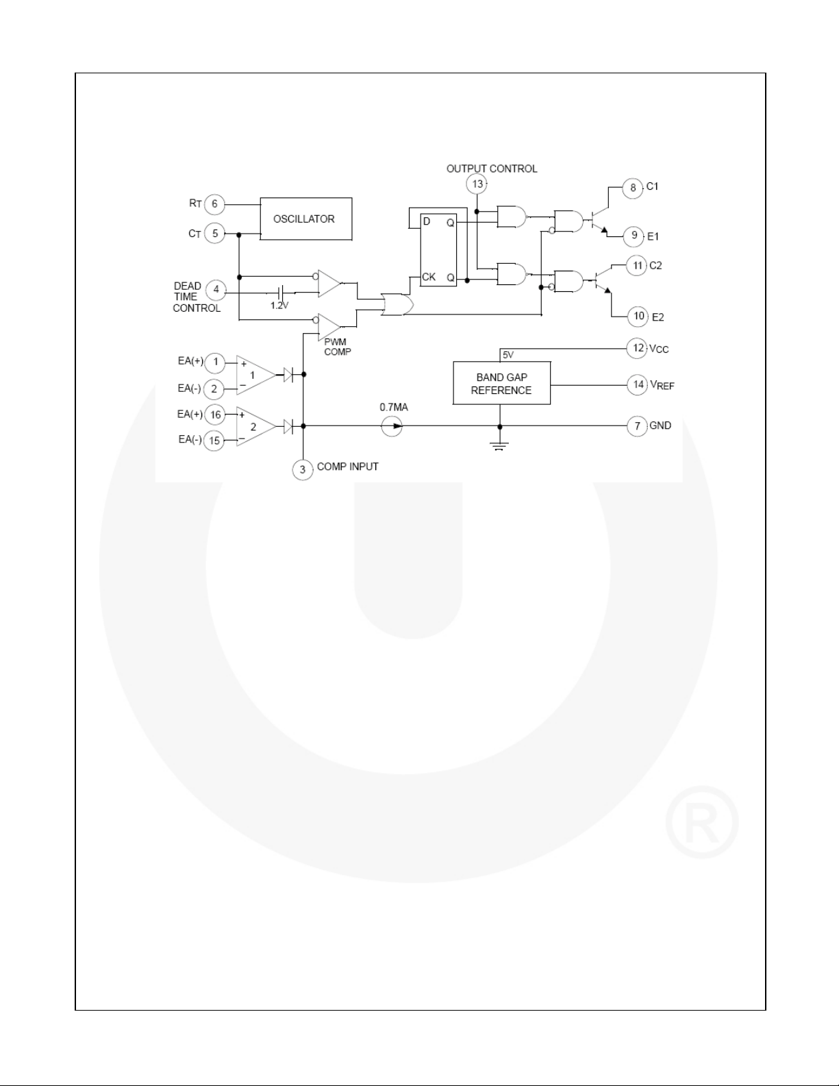
Block Diagram
KA7500C — SMPS Controller
Figure 1. Block Diagram
© 2003 Fairchild Semiconductor Corporation www.fairchildsemi.com
KA7500C • Rev. 1.0.2 2

Typical Application
VI=10V to 40V
47
KA7500C — SMPS Controller
KSA1010
Ω
Ω
150
0.1µF
1M
Ω
1mH, 2A
VO=5V
IO=1A
50 µ F
10 V
+
12
V
CC
D.T4GN D7E1
+
50V
11
C2
9
KA7500C
E2
10
C1
8
O.C
13
3
COMP IN PUT
R
T
6
47K
-
2
V
14
REF
-15
+1
+16
C
T
5
+50µF
Ω
0.001µF
150
5.1K
Ω
5. 1 K
Ω
5.1K
Ω
Ω
500µF
10V
+
GND
0.1
Figure 2. Pulse-Width Modulated Step-Down Converter
© 2003 Fairchild Semiconductor Corporation www.fairchildsemi.com
KA7500C • Rev. 1.0.2 3

Absolute Maximum Ratings
Stresses exceeding the absolute maximum ratings may damage the device. The device may not function or be
operable above the recommended operating conditions and stressing the parts to these levels is not recommended.
In addition, extended exposure to stresses above the recommended operating conditions may affect device
reliability. The absolute maximum ratings are stress ratings only.
Symbol Parameter Min. Max. Unit
VCC Supply Voltage 42 V
VC Collector Supply Voltage 42 V
IO Output Current 250 mA
VIN Amplifier Input Voltage VCC + 0.3 V
PD Power Dissipation
T
Operation Temperature Range -25 +85 °C
OPR
T
Storage Temperature Rang -65 +150 °C
STG
TJ Junction Temperature +125 °C
KA7500C 1
KA7500CD 0.9
W
KA7500C — SMPS Controller
Recommended Operating Conditions
The Recommended Operating Conditions table defines the conditions for actual device operation. Recommended
operating conditions are specified to ensure optimal performance to the datasheet specifications. Fairchild does not
recommend exceeding them or designing to Absolute Maximum Ratings.
Symbol Parameter Min. Typ. Max. Unit
VCC Power Supply Voltage 7 15 40 V
VC1, VC2 Collector Supply Voltage 30 40 V
IC1, IC2 Collector Output Current (Each Transition) 200 mA
VIN Amplifier Input Voltage 0.3 VCC - 2.0 V
IFB Current Into Feedback Terminal 0.3 mA
I
Reference Output Terminal 10 mA
REF
RT Timing Resistor 1.8 30.0 500.0
CT Timing Capacitor 0.0047 0.0010 10.0000 µA
f
Oscillator Frequency 1 40 200 kHz
OSC
V
PWM Input Voltage (Pins 3, 4, and 13) 0.3 5.3 V
IN_PWM
KΩ
© 2003 Fairchild Semiconductor Corporation www.fairchildsemi.com
KA7500C • Rev. 1.0.2 4

KA7500C — SMPS Controller
Electrical Characteristics
VCC = 20V, f = 10kHz, TA = -25°C to +85°C, unless otherwise specified.
Symbol Parameter Conditions Min. Typ. Max. Units
Reference Section
I
=1mA, TA=25°C
V
Reference Output Voltage
REF
R
Line Regulation VCC=7V to 40V 2 25 mV
LINE
R
Load Regulation I
LOAD
ISC Short-Circuit Output Current V
REF
I
=1mA 4.90 5.00 5.10
REF
=1mA to 10mA 1 15 mV
REF
=0V 10 35 50 mA
REF
Oscillation Frequency
CT=0.001µF, RT=30KΩ
CT=0.01µF, RT=12KΩ,
f
Oscillation Frequency
OSC
T
=25°C
A
CT=0.01µF, RT=12KΩ,
Δf/Δt
Frequency Change with Temperature
T
CT=0.01µF, RT=12KΩ
A=TLOW
to T
Dead-Time Control Section
I
Input Bias Current
BIAS
D
Maximum Duty Cycle
(MAX)
V
Input Threshold Voltage
ITH
Error Amplifier Section
VIO Input Offset Voltage V3=2.5V 2 10 mV
IIO Input Offset Current V3=2.5V 25 250 mA
I
Input Bias Current V3=2.5V 0.2 1.0 µA
BIAS
V
Common Mode Input Voltage
CIM
GVO Open-Loop Voltage Gain
BW Unit-Gain Bandwidth 650 kHz
PWM Comparator Section
V
Input Threshold Voltage Zero Duty Cycle 4.0 4.5 V
ITH
I
Input Sink Current V3=0.7V -0.3 -0.7 mA
SINK
Output Section
V
CE(SAT)
V
CC(SAT)
I
C(OFF)
I
E(OFF)
Output Saturation Voltage Common
Emitter
Emitter-Follower VC=15V, IE=-200mA 1.5 2.5
Collector Off-State Current VCC=40V, VCE=40V 2 100
Emitter Off-State Current VCC=VC=40V, VE=40V -100
Total Device
ICC Supply Current Pin6=V
Output Switching Characteristics
tR
tF
Rise Time, Common Emitter,
Common Collector
Fall Time, Common Emitter,
Common Collector
Note:
1. This is guaranteed where the marking code of the package surface is over 027.
VCC=15V, 0V≤ V4≤ 5.25V
VCC=15V, V4=0V, OC
Pin=V
REF
Zero Duty Cycle 3.0 3.3
Maximum Duty Cycle 0
7V≤ V
CC
≤ 40V
0.5V≤ V3 ≤ 3.5V
VE=0V, IC=200mA 1.0 1.3
, VCC=15V 6 10 mA
REF
100 200
25 100
HIGH
(1)
4.95 5.00 5.05
40.0
9.2 10.0 10.8
9.0 12.0
2 %
-2 -10 µA
45 %
-0.3 VCC V
70 95 dB
V
kHz
V
V
µA
ns
© 2003 Fairchild Semiconductor Corporation www.fairchildsemi.com
KA7500C • Rev. 1.0.2 5

10.10
9.70
A
6.00
B
0.30
1.80 MAX
1
1.27
9.08
8.68
TOP VIEW
916
8
0.51
0.36
M
0.20
1.65
1.45
0.05 MIN
B
4.15
3.75
C
B
B A
C
0.10
0.65
3.85 7.35
1.75
1.27
LAND PATTERN RECOMMENDATION
R0.20
A
C
0.303
0.153
B
GAGE
PLANE
0.36
FRONT VIEW
SEATING
PLANE
DETAIL A
SCALE 3:1
8°
0.90
0.50
R0.10
SIDE VIEW
NOTES:
A. THIS DRAWING COMPLIES WITH JEDEC
MS-012, EXCEPT AS NOTED
B
THIS DIMENSION IS OUTSIDE JEDEC
MS-012 VALUE
C. ALL DIMENSIONS ARE IN MILLIMETERS
D. DIMENSIONS ARE EXCLUSIVE OF BURRS,
MOLD FLASH, AND TIE BAR EXTRUSIONS
E. LAND PATTERN STANDARD:
SOIC127P600X175-16AM
F. DRAWING FILENAME: MKT-M16Erev2

A
16
19.69
18.67
9
7.11
6.10
5.33 MAX
C
0.38 MIN
NOTES:
1 8
B
(0.40)
TOP VIEW
1.78
1.14
4.95
2.92
3.81
2.92
0.56
2.54
0.36
0.25
M
C
FRONT VIEW
A. CONFORMS TO JEDEC MS-001, VARIATION BB
B. ALL DIMENSIONS ARE IN MILLIMETERS
C. DIMENSIONS ARE EXCLUSIVE OF BURRS,
MOLD FLASH, AND TIE BAR PROTRUSIONS
D. DIMENSIONS AND TOLERANCES PER ASME
Y14.5M-2009
E. DRAWING FILENAME: MKT-N16Erev3
8.25
7.62
0.28
0.20
10.92
SIDE VIEW

ON Semiconductor and are trademarks of Semiconductor Components Industries, LLC dba ON Semiconductor or its subsidiaries in the United States and/or other countries.
ON Semiconductor owns the rights to a number of patents, trademarks, copyrights, trade secrets, and other intellectual property. A listing of ON Semiconductor’s product/patent
coverage may be accessed at www.onsemi.com/site/pdf/Patent−Marking.pdf
ON Semiconductor makes no warranty, representation or guarantee regarding the suitability of its products for any particular purpose, nor does ON Semiconductor assume any liability
arising out of the application or use of any product or circuit, and specifically disclaims any and all liability, including without limitation special, consequential or incidental damages.
Buyer is responsible for its products and applications using ON Semiconductor products, including compliance with all laws, regulations and safety requirements or standards,
regardless of any support or applications information provided by ON Semiconductor. “Typical” parameters which may be provided in ON Semiconductor data sheets and/or
specifications can and do vary in different applications and actual performance may vary over time. All operating parameters, including “Typicals” must be validated for each customer
application by customer’s technical experts. ON Semiconductor does not convey any license under its patent rights nor the rights of others. ON Semiconductor products are not
designed, intended, or authorized for use as a critical component in life support systems or any FDA Class 3 medical devices or medical devices with a same or similar classification
in a foreign jurisdiction or any devices intended for implantation in the human body. Should Buyer purchase or use ON Semiconductor products for any such unintended or unauthorized
application, Buyer shall indemnify and hold ON Semiconductor and its officers, employees, subsidiaries, affiliates, and distributors harmless against all claims, costs, damages, and
expenses, and reasonable attorney fees arising out of, directly or indirectly, any claim of personal injury or death associated with such unintended or unauthorized use, even if such
claim alleges that ON Semiconductor was negligent regarding the design or manufacture of the part. ON Semiconductor is an Equal Opportunity/Affirmative Action Employer. This
literature is subject to all applicable copyright laws and is not for resale in any manner.
. ON Semiconductor reserves the right to make changes without further notice to any products herein.
PUBLICATION ORDERING INFORMATION
LITERATURE FULFILLMENT:
Literature Distribution Center for ON Semiconductor
19521 E. 32nd Pkwy, Aurora, Colorado 80011 USA
Phone: 303−675−2175 or 800−344−3860 Toll Free USA/Canada
Fax: 303−675−2176 or 800−344−3867 Toll Free USA/Canada
Email: orderlit@onsemi.com
© Semiconductor Components Industries, LLC
N. American Technical Support: 800−282−9855 Toll Free
USA/Canada
Europe, Middle East and Africa Technical Support:
Phone: 421 33 790 2910
Japan Customer Focus Center
Phone: 81−3−5817−1050
www.onsemi.com
ON Semiconductor Website: www.onsemi.com
Order Literature: http://www.onsemi.com/orderlit
For additional information, please contact your local
Sales Representative
www.onsemi.com
1

 Loading...