

ESD9M5.0ST5G
Transient Voltage
Suppressors
ESD Protection Diodes with Ultra−Low
Capacitance
The ESD9M Series is designed to protect voltage sensitive components
that require low capacitance from ESD and transient voltage events.
Excellent clamping capability, low capacitance, low leakage, and fast
response time, make these parts ideal for ESD protection on designs that
utilize high−speed lines such as USB.
Specification Features:
• Low Capacitance 2.5 pF
• Low Clamping Voltage
• Small Body Outline Dimensions:
0.039″ x 0.024″ (1.00 mm x 0.60 mm)
• Low Body Height: 0.016″ (0.4 mm)
• Stand−off Voltage: 5 V
• Low Leakage
• Response Time is Typically < 1.0 ns
• IEC61000−4−2 Level 4 ESD Protection
• This is a Pb−Free Device
Mechanical Characteristics:
CASE:
Void-free, transfer-molded, thermosetting plastic
Epoxy Meets UL 94 V−0
LEAD FINISH: 100% Matte Sn (Tin)
MOUNTING POSITION: Any
QUALIFIED MAX REFLOW TEMPERATURE: 260°C
Device Meets MSL 1 Requirements
MAXIMUM RATINGS
Rating Symbol Value Unit
IEC 61000−4−2 (ESD) Contact
Total Power Dissipation on FR−5 Board
(Note 1) @ T
Junction and Storage Temperature Range TJ, T
Lead Solder Temperature − Maximum
(10 Second Duration)
Stresses exceeding Maximum Ratings may damage the device. Maximum
Ratings are stress ratings only. Functional operation above the Recommended
Operating Conditions is not implied. Extended exposure to stresses above the
Recommended Operating Conditions may affect device reliability.
1. FR−5 = 1.0 x 0.75 x 0.62 in.
= 25°C
A
Air
°PD° 150 mW
stg
T
L
±10
±15
−55 to
+150
260 °C
kV
°C
http://onsemi.com
SOD−923
CASE 514AB
MARKING DIAGRAM
4 M
4 = Specific Device Code
M = Date Code
ORDERING INFORMATION
Device Package Shipping
ESD9M5.0ST5G SOD−923
†For information on tape and reel specifications,
including part orientation and tape sizes, please
refer to our Tape and Reel Packaging Specifications
Brochure, BRD8011/D.
DEVICE MARKING INFORMATION
See specific marking information in the device marking
column of the Electrical Characteristics tables starting on
page 2 of this data sheet.
(Pb−Free)
8000/Tape & Reel
†
See Application Note AND8308/D for further description of survivability specs.
© Semiconductor Components Industries, LLC, 2009
January, 2009 − Rev. 4
1 Publication Order Number:
ESD9M5.0S/D
ESD9M5.0ST5G
ELECTRICAL CHARACTERISTICS
(TA = 25°C unless otherwise noted)
Symbol
V
I
V
RWM
V
V
P
Maximum Reverse Peak Pulse Current
PP
Clamping Voltage @ I
C
Working Peak Reverse Voltage
I
Maximum Reverse Leakage Current @ V
R
Breakdown Voltage @ I
BR
I
Test Current
T
I
Forward Current
F
Forward Voltage @ I
F
Peak Power Dissipation
pk
C Max. Capacitance @ VR = 0 and f = 1.0 MHz
Parameter
PP
T
F
RWM
VCV
V
RWM
BR
Uni−Directional TVS
*See Application Note AND8308/D for detailed explanations of
datasheet parameters.
ELECTRICAL CHARACTERISTICS (T
= 25°C unless otherwise noted, VF = 1.0 V Max. @ IF = 10 mA for all types)
A
V
RWM
(V)
I
R
@ V
(mA)
RWM
VBR (V) @ I
(Note 2)
T
I
C (pF)
T
Device
Device
Marking
Max Max Min mA Max Max
ESD9M5.0ST5G 4* 5.0 1.0 5.8 1.0 2.5 9.8 Figures1and 2
* Rotated 270°.
* *The “G’’ suffix indicates Pb−Free package available.
***Other voltages available upon request.
2. V
is measured with a pulse test current IT at an ambient temperature of 25°C.
BR
3. For test procedure see Figures 3 and 4 and Application Note AND8307/D.
4. Surge current waveform per Figure 5.
I
F
VC (V)
@ I
PP
(Note 4)
I
I
R
I
T
I
PP
= 1 A
V
F
V
V
C
Per IEC61000−4−2
(Note 3)
See Below
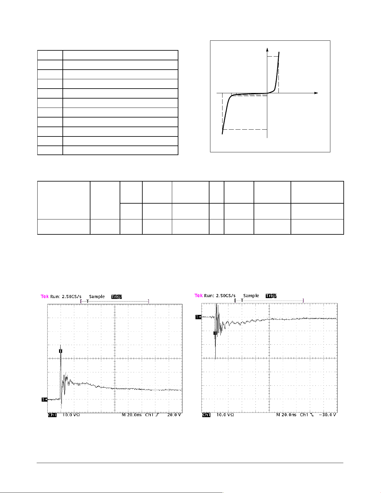
Figure 1. ESD Clamping Voltage Screenshot
Positive 8 kV Contact per IEC61000−4−2
http://onsemi.com
Figure 2. ESD Clamping Voltage Screenshot
Negative 8 kV Contact per IEC61000−4−2
2

ESD9M5.0ST5G
IEC 61000−4−2 Spec.
Test
Voltage
Level
1 2 7.5 4 2
2 4 15 8 4
3 6 22.5 12 6
4 8 30 16 8
(kV)
ESD Gun
First Peak
Current
(A)
Current at
30 ns (A)
TVS
50 W
Cable
IEC61000−4−2 Waveform
I
peak
Current at
60 ns (A)
100%
90%
I @ 30 ns
I @ 60 ns
10%
Figure 3. IEC61000−4−2 Spec
Oscilloscope
50 W
tP = 0.7 ns to 1 ns
Figure 4. Diagram of ESD Test Setup
The following is taken from Application Note
AND8308/D − Interpretation of Datasheet Parameters
for ESD Devices.
ESD Voltage Clamping
For sensitive circuit elements it is important to limit the
voltage that an IC will be exposed to during an ESD event
to as low a voltage as possible. The ESD clamping voltage
is the voltage drop across the ESD protection diode during
an ESD event per the IEC61000−4−2 waveform. Since the
IEC61000−4−2 was written as a pass/fail spec for larger
100
t
r
90
80
70
60
50
40
30
20
% OF PEAK PULSE CURRENT
10
0
020406080
PEAK VALUE I
t
P
Figure 5. 8 X 20 ms Pulse Waveform
systems such as cell phones or laptop computers it is not
clearly defined in the spec how to specify a clamping voltage
at the device level. ON Semiconductor has developed a way
to examine the entire voltage waveform across the ESD
protection diode over the time domain of an ESD pulse in the
form of an oscilloscope screenshot, which can be found on
the datasheets for all ESD protection diodes. For more
information on how ON Semiconductor creates these
screenshots and how to interpret them please refer to
AND8307/D.
@ 8 ms
RSM
PULSE WIDTH (tP) IS DEFINED
AS THAT POINT WHERE THE
PEAK CURRENT DECAY = 8 ms
HALF VALUE I
t, TIME (ms)
/2 @ 20 ms
RSM
http://onsemi.com
3

ESD9M5.0ST5G
PACKAGE DIMENSIONS
SOD−923
CASE 514AB−01
ISSUE B
−X−
D
−Y−
E
21
2X
b
0.08 (0.0032)
XY
A
c
H
E
L
SOLDERING FOOTPRINT*
NOTES:
1. DIMENSIONING AND TOLERANCING PER ANSI
Y14.5M, 1982.
2. CONTROLLING DIMENSION: MILLIMETERS.
3. MAXIMUM LEAD THICKNESS INCLUDES LEAD
FINISH THICKNESS. MINIMUM LEAD
THICKNESS IS THE MINIMUM THICKNESS OF
BASE MATERIAL.
MILLIMETERS
DIM MIN NOM MAX
A 0.34 0.37 0.40
b 0.15 0.20 0.25
c 0.07 0.12 0.17
D 0.75 0.80 0.85
E 0.55 0.60 0.65
H
0.95 1.00 1.05
E
L 0.05 0.10 0.15
INCHES
MIN NOM MAX
0.013 0.015 0.016
0.006 0.008 0.010
0.003 0.005 0.007
0.030 0.031 0.033
0.022 0.024 0.026
0.037 0.039 0.041
0.002 0.004 0.006
0.90
0.40
0.30
DIMENSIONS: MILLIMETERS
*For additional information on our Pb−Free strategy and soldering
details, please download the ON Semiconductor Soldering and
Mounting Techniques Reference Manual, SOLDERRM/D.
ON Semiconductor and are registered trademarks of Semiconductor Components Industries, LLC (SCILLC). SCILLC reserves the right to make changes without further notice
to any products herein. SCILLC makes no warranty, representation or guarantee regarding the suitability of its products for any particular purpose, nor does SCILLC assume any liability
arising out of the application or use of any product or circuit, and specifically disclaims any and all liability, including without limitation special, consequential or incidental damages.
“Typical” parameters which may be provided in SCILLC data sheets and/or specifications can and do vary in different applications and actual performance may vary over time. All
operating parameters, including “Typicals” must be validated for each customer application by customer’s technical experts. SCILLC does not convey any license under its patent rights
nor the rights of others. SCILLC products are not designed, intended, or authorized for use as components in systems intended for surgical implant into the body, or other applications
intended to support or sustain life, or for any other application in which the failure of the SCILLC product could create a situation where personal injury or death may occur. Should
Buyer purchase or use SCILLC products for any such unintended or unauthorized application, Buyer shall indemnify and hold SCILLC and its officers, employees, subsidiaries, affiliates,
and distributors harmless against all claims, costs, damages, and expenses, and reasonable attorney fees arising out of, directly or indirectly, any claim of personal injury or death
associated with such unintended or unauthorized use, even if such claim alleges that SCILLC was negligent regarding the design or manufacture of the part. SCILLC is an Equal
Opportunity/Affirmative Action Employer. This literature is subject to all applicable copyright laws and is not for resale in any manner.
PUBLICATION ORDERING INFORMATION
LITERATURE FULFILLMENT:
Literature Distribution Center for ON Semiconductor
P.O. Box 5163, Denver, Colorado 80217 USA
Phone: 303−675−2175 or 800−344−3860 Toll Free USA/Canada
Fax: 303−675−2176 or 800−344−3867 Toll Free USA/Canada
Email: orderlit@onsemi.com
N. American Technical Support: 800−282−9855 Toll Free
USA/Canada
Europe, Middle East and Africa Technical Support:
Phone: 421 33 790 2910
Japan Customer Focus Center
Phone: 81−3−5773−3850
http://onsemi.com
4
ON Semiconductor Website: www.onsemi.com
Order Literature: http://www.onsemi.com/orderlit
For additional information, please contact your local
Sales Representative
ESD9M5.0S/D

 Loading...