

DF3A6.8FUT1
Preferred Device
Zener Transient Voltage
Suppressor
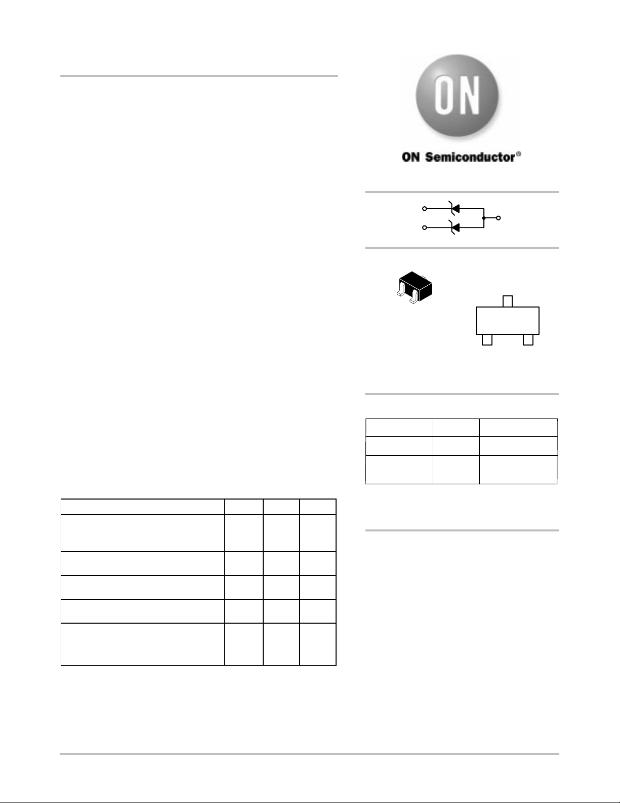
Dual Common Anode Zeners for ESD
Protection
These dual monolithic silicon zener diodes are designed for
applications requiring transient overvoltage protection capability. They
are intended for use in voltage and ESD sensitive equipment such as
computers, printers, business machines, communication systems,
medical equipment and other applications. Their d ual junction common
anode design protects two separate lines using only o ne p ackage. T hese
devices are ideal for situations where board space is at a premium.
Features
• Pb−Free Package is Available
• SC−70 Package Allows Two Separate Unidirectional Configurations
• Low Leakage < 1.0 A @ 5.0 V
• Breakdown Voltage: 6.4−7.2 V @ 5.0 mA
• ESD Protection Meeting:16 kV Human Body Model
30 kV Contact = IEC61000−4−2
• Peak Power: 24 W @ 1.0 ms (Unidirectional), per Figure 1
• Peak Power: 150 W @ 20 s (Unidirectional), per Figure 2
Mechanical Characteristics
• Void Free, Transfer−Molded, Thermosetting Plastic Case
• Corrosion Resistant Finish, Easily Solderable
• Package Designed for Optimal Automated Board Assembly
• Small Package Size for High Density Applications
MAXIMUM RATINGS
Rating Symbol Value Unit
Steady State Power Dissipation
Derate above 25°C (Note 1)
Thermal Resistance Junction−to−Ambient R
Operating Junction and Storage
Temperature Range
Peak Power Dissipation @ 1.0 ms
(Note 2) @ T
Peak Power Dissipation @ 20 s (Note 3)
= 25°C
@ T
A
ESD Discharge
MIL STD 883C − Method 3015−6
IEC61000−4−2, Air Discharge
IEC61000−4−2, Contact Discharge
Maximum ratings are those values beyond which device damage can occur.
Maximum ratings applied to the device are individual stress limit values (not
normal operating conditions) and are not valid simultaneously. If these limits
are exceeded, device functional operation is not implied, damage may occur
and reliability may be affected.
1. Mounted on FR−5 Board = 1.0 X 0.75 X 0.062 in.
2. Non−repetitive pulse per Figure 1.
3. Non−repetitive pulse per Figure 2.
= 25°C
A
P
TJ, T
P
P
V
stg
200
1.6
618 °C/W
− 55 to
+150
20 W
150 W
16
30
30
D
JA
PK
PK
PP
°mW°
mW/°C
°C
kV
http://onsemi.com
1
2
3
MARKING
DIAGRAM
1
2
SC−70/SOT−323
CASE 419
STYLE 4
68
68 = Specific Device Code
M = Date Code
M
ORDERING INFORMATION
Device Package Shipping
DF3A6.8FUT1 SC−70 3000/Tape & Reel
DF3A6.8FUT1G SC−70
(Pb−Free)
†For information on tape and reel specifications,
including part orientation and tape sizes, please
refer to our Tape and Reel Packaging Specifications
Brochure, BRD8011/D.
Preferred devices are recommended choices for future use
and best overall value.
3000/Tape & Reel
†
Semiconductor Components Industries, LLC, 2004
July, 2004 − Rev. 1
1 Publication Order Number:
DF3A6.8FUT1/D
DF3A6.8FUT1
ELECTRICAL CHARACTERISTICS
(TA = 25°C unless otherwise noted)
UNIDIRECTIONAL (Circuit tied to Pins 1 and 3 or 2 and 3)
Symbol
V
RWM
I
V
I
I
V
Z
Z
Working Peak Reverse Voltage
Maximum Reverse Leakage Current @ V
R
Breakdown Voltage @ I
BR
Test Current
T
Forward Current
F
Forward Voltage @ I
F
Maximum Zener Impedance @ I
ZT
Maximum Zener Impedance @ I
ZK
ELECTRICAL CHARACTERISTICS (T
Parameter
T
F
RWM
ZT
ZK
= 25°C unless otherwise noted)
A
UNIDIRECTIONAL (Circuit tied to Pins 1 and 3 or 2 and 3)
Parameter
Forward Voltage V
Zener Voltage (Note 4) V
Operating Resistance (Note 5) Z
Reverse Current I
Clamping Voltage V
ESD Protection
Human Body Model (HBM)
Contact − IEC61000−4−2
Air Discharge
4. VZ measured at pulse test current IZT at an ambient temperature of 25°C.
5. Z
ZT
and Z
is measured by dividing the AC voltage drop across the device by the AC current supplied. AC frequency = 1.0 kHz.
ZK
Symbol Conditions Min Typ Max Unit
IF = 10 mA 0.8 0.9 V
F
IZT = 5 mA 6.4 6.8 7.2 V
Z
ZK
Z
ZT
R1
IZK = 0.5 mA 200
IZT = 5 mA 50
V
= 5 V 0.5 A
RWM
IPP = 2.0 A (Figure 1)
C
I
= 9.37 A (Figure 2)
PP
VCV
V
RWM
BR
Uni−Directional TVS
I
I
F
I
V
R
F
I
T
I
PP
9.6
16
V
V
V
kV
16
30
30
http://onsemi.com
2

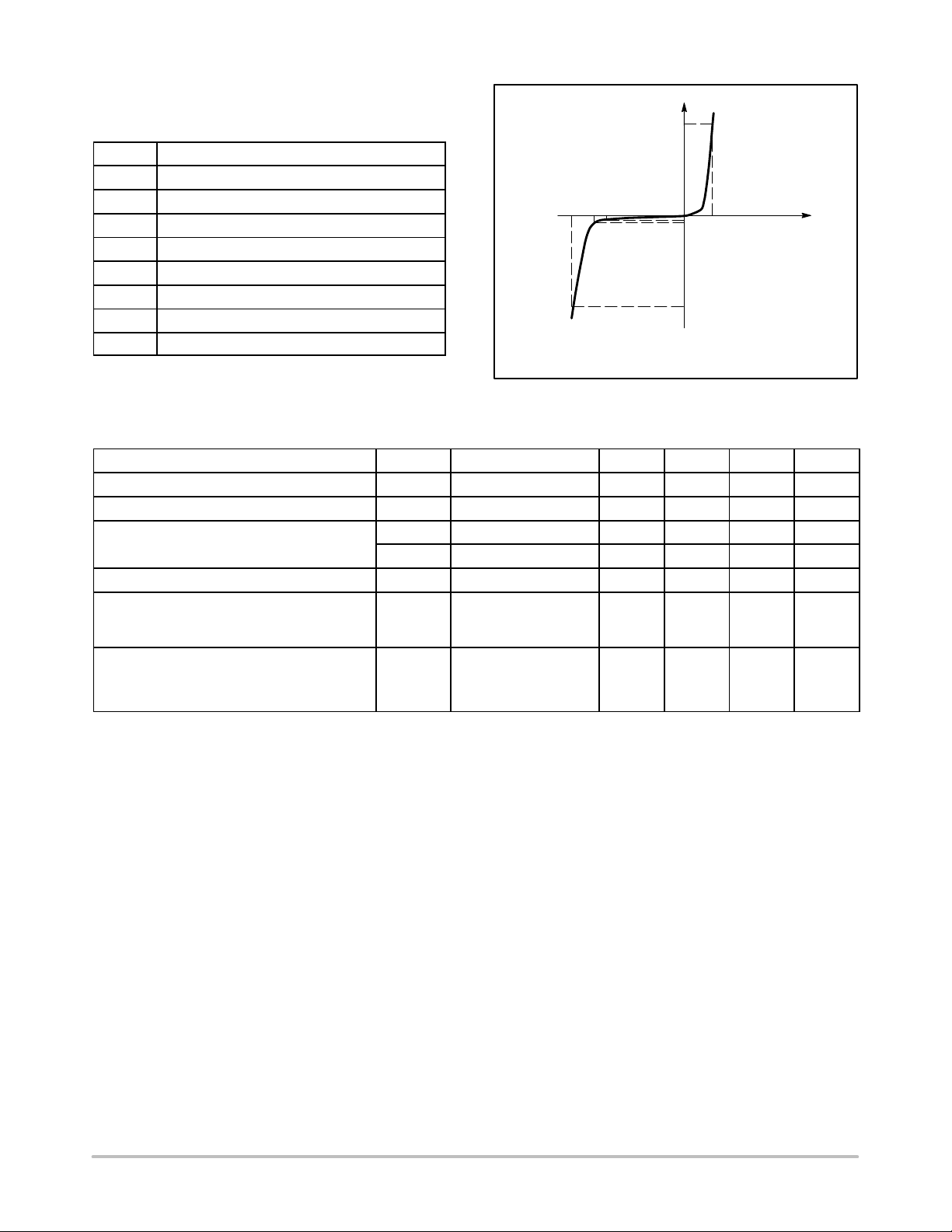
TYPICAL CHARACTERISTICS
PULSE WIDTH (tP) IS
t
r
100
VALUE (%)
50
PEAK VALUE— I
t
P
0
01234
RSM
HALF VALUE—
t, TIME (ms)
Figure 1. 10 × 1000 s Pulse Waveform
DEFINED AS THAT POINT
WHERE THE PEAK
CURRENT DECAYS TO
50%OF I
t
≤ 10 s
r
I
RS
2
M
RSM
DF3A6.8FUT1
.
100
90
80
70
60
50
t
r
PEAK VALUE I
RSM
@ 8 s
PULSE WIDTH (tP) IS DEFINED
AS THAT POINT WHERE THE
PEAK CURRENT DECAY = 8 s
HALF VALUE I
RSM
/2 @ 20 s
40
30
20
% OF PEAK PULSE CURRENT
t
P
10
0
020406080
t, TIME (s)
Figure 2. 8 × 20 s Pulse Waveform
20.01
18.01
16.01
REVERSE VOLTAGE IS
MEASURED WITH A PULSE
TEST CURRENT I
AT 25°C
T
14.01
12.01
10.01
8.01
, ZENER CURRENT (mA)
6.01
ZT
I
4.01
2.01
0
6 6.2 6.4 6.6 6.8 7 7.2 8
7.4 7.6 7.8
VZ, ZENER VOLTAGE (V)
Figure 3. Zener Voltage vs. Zener Current Figure 4. Forward Voltage vs. Forward
100
90
80
70
60
UniDirectional Pin 1/2−3
50
40
C, CAPACITANCE (pF)
30
BiDirectional Pin 1−2
20
10
0
012345 6
V, BIAS VOLTAGE (V)
f = 1 MHz
T
= 25°C
A
200
FORWARD VOLTAGE IS
180
MEASURED WITH A PULSE
160
TEST CURRENT I
AT 25°C
F
140
120
100
80
60
, FORWARD CURRENT (mA)
F
40
I
20
0
0.5 0.6 0.7 0.8 0.9 1.0 1.1 1.2
VF, FORWARD VOLTAGE (V)
Current
300
250
200
150
100
, POWER DISSIPATION (mW)
D
P
50
0
0 25 50 75 100 125 150 175
T
, AMBIENT TEMPERATURE (°C)
A
Figure 5. Capacitance vs. Bias Voltage Figure 6. Steady State Power Derating Curve
http://onsemi.com
3

DF3A6.8FUT1
PACKAGE DIMENSIONS
SC−70 (SOT−323)
CASE 419−04
ISSUE L
0.05 (0.002)
A
L
3
S
12
G
H
B
D
C
N
SOLDERING FOOTPRINT*
0.65
0.025
NOTES:
1. DIMENSIONING AND TOLERANCING PER ANSI
Y14.5M, 1982.
2. CONTROLLING DIMENSION: INCH.
DIM MIN MAX MIN MAX
A 0.071 0.087 1.80 2.20
B 0.045 0.053 1.15 1.35
C 0.032 0.040 0.80 1.00
D 0.012 0.016 0.30 0.40
G 0.047 0.055 1.20 1.40
H 0.000 0.004 0.00 0.10
J 0.004 0.010 0.10 0.25
K 0.017 REF 0.425 REF
L 0.026 BSC 0.650 BSC
N 0.028 REF 0.700 REF
S 0.079 0.095 2.00 2.40
J
K
STYLE 4:
PIN 1. CATHODE
2. CATHODE
3. ANODE
MILLIMETERSINCHES
0.65
0.025
1.9
0.075
0.9
0.035
0.7
0.028
SCALE 10:1
inches
mm
*For additional information on our Pb−Free strategy and soldering
details, please download the ON Semiconductor Soldering and
Mounting Techniques Reference Manual, SOLDERRM/D.
ON Semiconductor and are registered trademarks of Semiconductor Components Industries, LLC (SCILLC). SCILLC reserves the right to make changes without further notice
to any products herein. SCILLC makes no warranty, representation or guarantee regarding the suitability of its products for any particular purpose, nor does SCILLC assume any liability
arising out of the application or use of any product or circuit, and specifically disclaims any and all liability, including without limitation special, consequential or incidental damages.
“Typical” parameters which may be provided in SCILLC data sheets and/or specifications can and do vary in different applications and actual performance may vary over time. All
operating parameters, including “Typicals” must be validated for each customer application by customer’s technical experts. SCILLC does not convey any license under its patent rights
nor the rights of others. SCILLC products are not designed, intended, or authorized for use as components in systems intended for surgical implant into the body, or other applications
intended to support or sustain life, or for any other application in which the failure of the SCILLC product could create a situation where personal injury or death may occur. Should
Buyer purchase or use SCILLC products for any such unintended or unauthorized application, Buyer shall indemnify and hold SCILLC and its officers, employees, subsidiaries, affiliates,
and distributors harmless against all claims, costs, damages, and expenses, and reasonable attorney fees arising out of, directly or indirectly, any claim of personal injury or death
associated with such unintended or unauthorized use, even if such claim alleges that SCILLC was negligent regarding the design or manufacture of the part. SCILLC is an Equal
Opportunity/Affirmative Action Employer. This literature is subject to all applicable copyright laws and is not for resale in any manner.
PUBLICATION ORDERING INFORMATION
LITERATURE FULFILLMENT:
Literature Distribution Center for ON Semiconductor
P.O. Box 61312, Phoenix, Arizona 85082−1312 USA
Phone: 480−829−7710 or 800−344−3860 Toll Free USA/Canada
Fax: 480−829−7709 or 800−344−3867 Toll Free USA/Canada
Email: orderlit@onsemi.com
N. American Technical Support: 800−282−9855 Toll Free
USA/Canada
Japan: ON Semiconductor, Japan Customer Focus Center
2−9−1 Kamimeguro, Meguro−ku, Tokyo, Japan 153−0051
Phone: 81−3−5773−3850
http://onsemi.com
ON Semiconductor Website: http://onsemi.com
Order Literature: http://www.onsemi.com/litorder
For additional information, please contact your
local Sales Representative.
DF3A6.8FUT1/D
4

 Loading...