CM1692
Praetorian L-C LCD and
Camera EMI Filter Array
with ESD Protection
Features
• Four, Six and Eight Channels of EMI Filtering with Integrated
ESD Protection
• Pi−Style EMI Filters in a Capacitor−Inductor−Capacitor (C−L−C)
Network
• ±15 kV ESD Protection on Each Channel
(IEC 61000−4−2 Level 4, Contact Discharge)
• Greater than 30 dB Attenuation (Typical) at 1 GHz
• 0.50 mm Thick mDFN Package with 0.40 mm Lead Pitch:
♦ 4−channel = 8−lead mDFN
♦ 6−channel = 12−lead mDFN
♦ 8−channel = 16−lead mDFN
• Tiny mDFN Package Size:
♦ 8−lead: 1.70 mm x 1.35 mm
♦ 12−lead: 2.50 mm x 1.35 mm
♦ 16−lead: 3.30 mm x 1.35 mm
• These Devices are Pb−Free and are RoHS Compliant
Applications
• LCD and Camera Data Lines in Mobile Handsets
• Wireless Handsets
• LCD and Camera Modules
http://onsemi.com
UDFN8
DE SUFFIX
CASE 517BC
UDFN12
DE SUFFIX
CASE 517BD
UDFN16
DE SUFFIX
CASE 517BE
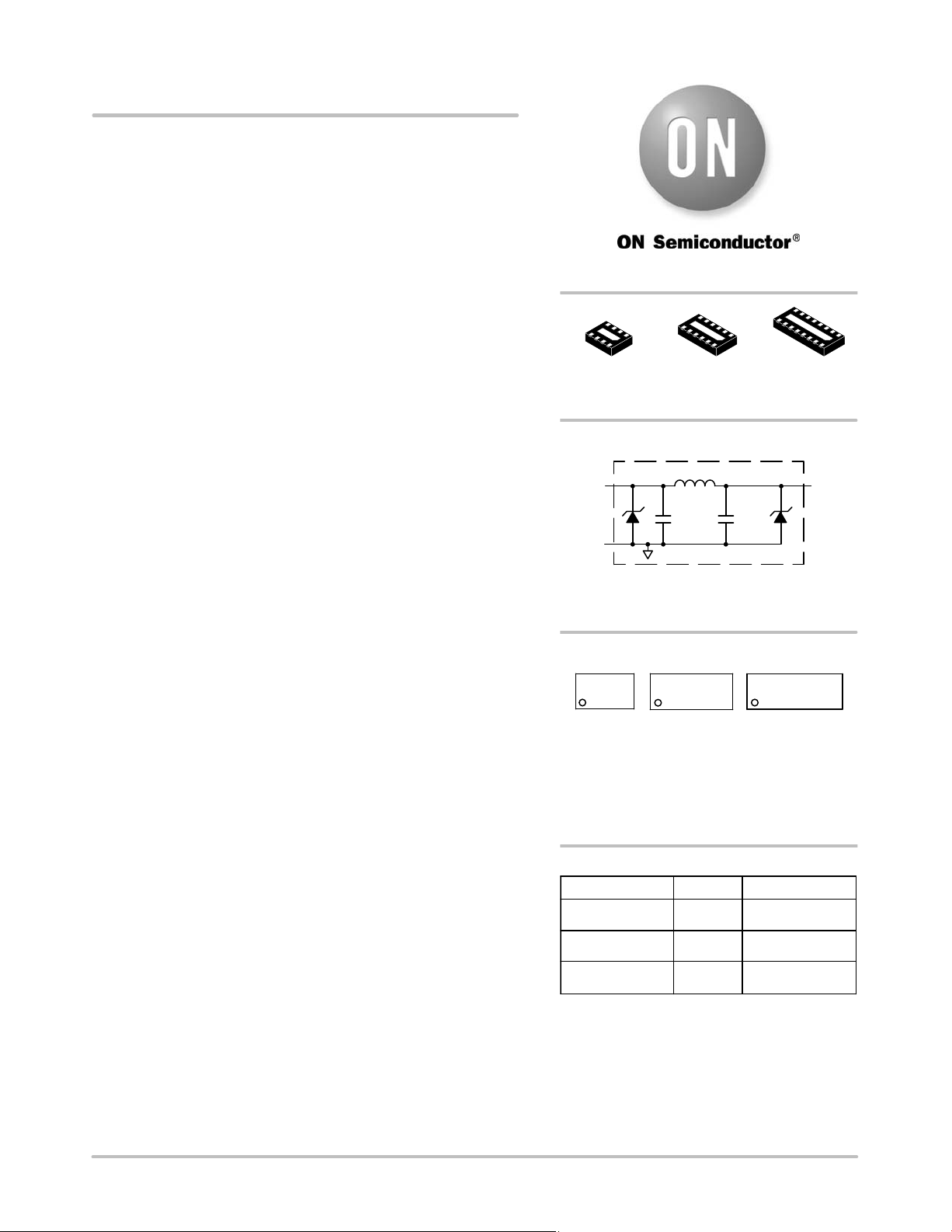
ELECTRICAL SCHEMATIC
Filter
+
ESDn*
GND
1 of 4, 6 or 8 EMI/RFI Filter Channels
with Integrated ESD Protection
* See Package/Pinout Diagrams for expanded pin information.
17 nH
12 pF12 pF
MARKING DIAGRAM
P92 MG
G
1
(Note: Microdot may be in either location)
P926 MG
G
1
P92 = CM1692−04DE
P926 = CM1692−06DE
P928 = CM1692−08DE
M = Date Code
G = Pb−Free Package
1
P928 MG
G
Filter
+
ESDn*
© Semiconductor Components Industries, LLC, 2011
April, 2011 − Rev. 4
ORDERING INFORMATION
Device Package Shipping
CM1692−04DE
CM1692−06DE
CM1692−08DE
†For information on tape and reel specifications,
including part orientation and tape sizes, please
refer to our Tape and Reel Packaging Specification
Brochure, BRD8011/D.
1 Publication Order Number:
mDFN−8
(Pb−Free)
mDFN−12
(Pb−Free)
mDFN−16
(Pb−Free)
3000/Tape & Reel
3000/Tape & Reel
3000/Tape & Reel
†
CM1692/D

CM1692
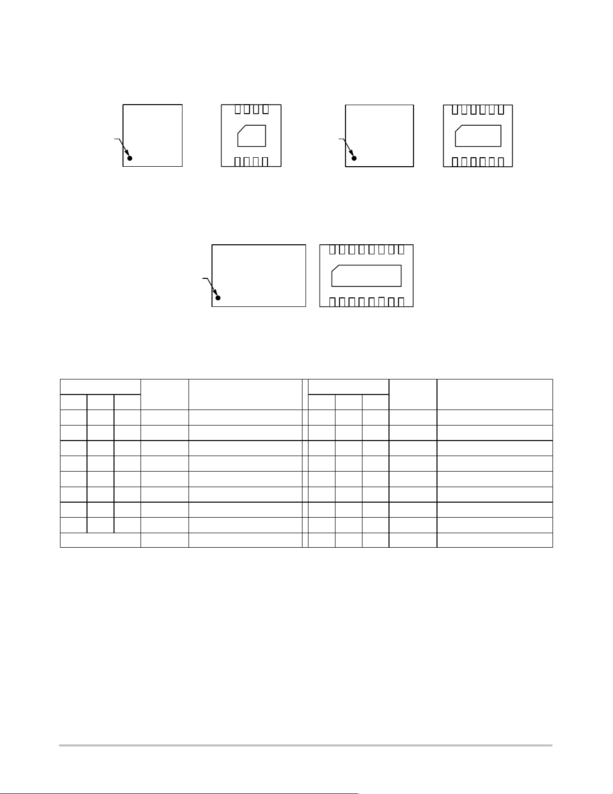
PACKAGE / PINOUT DIAGRAMS
Pin 1
Marking
Top View
(Pins Down View)
8765
P92
1234 8765
CM1692−04DE
8 Lead mDFN Package
Pin 1
Marking
Bottom View
(Pins Up View)
1234
(Pins Down View)
14 12
1516 1110 9
12345678
GND
PAD
Top View
13
P928
CM1692−08DE
16 Lead mDFN Package
(Pins Down View)
Pin 1
Marking
1 2 3 4 12 1110 956 87
Bottom View
(Pins Up View)
12345678
GND
PAD
1314 121516 1110 9
Top View
P926
CM1692−06DE
12 Lead mDFN Package
Bottom View
(Pins Up View)
123412 1110 9 5 687
GND
PAD
Table 1. PIN DESCRIPTIONS
Device Pin(s)
−04 −06 −08 −04 −06 −08
1 1 1 FILTER1 Filter + ESD Channel 1 8 12 16 FILTER1 Filter + ESD Channel 1
2 2 2 FILTER2 Filter + ESD Channel 2 7 11 15 FILTER2 Filter + ESD Channel 2
3 3 3 FILTER3 Filter + ESD Channel 3 6 10 14 FILTER3 Filter + ESD Channel 3
4 4 4 FILTER4 Filter + ESD Channel 4 5 9 13 FILTER4 Filter + ESD Channel 4
− 5 5 FILTER5 Filter + ESD Channel 5 − 8 12 FILTER5 Filter + ESD Channel 5
− 6 6 FILTER6 Filter + ESD Channel 6 − 7 11 FILTER6 Filter + ESD Channel 6
− − 7 FILTER7 Filter + ESD Channel 7 − − 10 FILTER7 Filter + ESD Channel 7
− − 8 FILTER8 Filter + ESD Channel 8 − − 9 FILTER8 Filter + ESD Channel 8
GND PAD GND Device Ground − − − −
Name Description
Device Pin(s)
Name Description
http://onsemi.com
2

CM1692
SPECIFICATIONS
Table 2. ABSOLUTE MAXIMUM RATINGS
Parameter Rating Units
Storage Temperature Range −65 to +150 °C
Current per Inductor 30 mA
DC Package Power Rating 500 mW
Stresses exceeding Maximum Ratings may damage the device. Maximum Ratings are stress ratings only. Functional operation above the
Recommended Operating Conditions is not implied. Extended exposure to stresses above the Recommended Operating Conditions may affect
device reliability.
Table 3. STANDARD OPERATING CONDITIONS
Parameter Rating Units
Operating Temperature Range –40 to +85 °C
Table 4. ELECTRICAL OPERATING CHARACTERISTICS (Note 1)
Symbol Parameter Conditions Min Ty p Max Units
L Channel Inductance 17 nH
C
TOTAL
C Capacitance C1 At 2.5 V DC Reverse Bias,
V
DIODE
I
LEAK
V
SIG
V
ESD
R
DYN
f
C
1. T
= 25°C unless otherwise specified.
A
2. ESD applied to input and output pins with respect to GND, one at a time.
3. Clamping voltage is measured at the opposite side of the EMI filter to the ESD pin (i.e. if ESD is applied to pin A1 then clamping voltage is
measured at pin C1). Unused pins are left open.
Total Channel Capacitance At 2.5 V DC Reverse Bias,
1 MHz, 30 mV AC
1 MHz, 30 mV AC
Stand−off Voltage
Diode Leakage Current (Reverse Bias) V
Signal Clamp Voltage
Positive Clamp
Negative Clamp
In−system ESD Withstand Voltage
I
= 10 mA
DIODE
= 3.3 V 0.1 1.0
DIODE
(Note 3)
I
= 10 mA
LOAD
I
= −10 mA
LOAD
(Notes 2 and 3)
Contact Discharge per
IEC 61000−4−2 Standard, Level 4
Dynamic Resistance
Positive
Negative
Roll−off Frequency at −6 dB Attenuation
Z
SOURCE
= 50 W, Z
LOAD
= 50 W
18.8 23.5 28.2 pF
11.8 pF
6.0 V
mA
5.6
6.8
−1.5
−0.8
9.0
−0.4
kV
±15
2.3
0.9
MHz
400
V
W
http://onsemi.com
3
 Loading...