CM1216
6 and 8-Channel Low
Capacitance ESD Arrays
Product Description
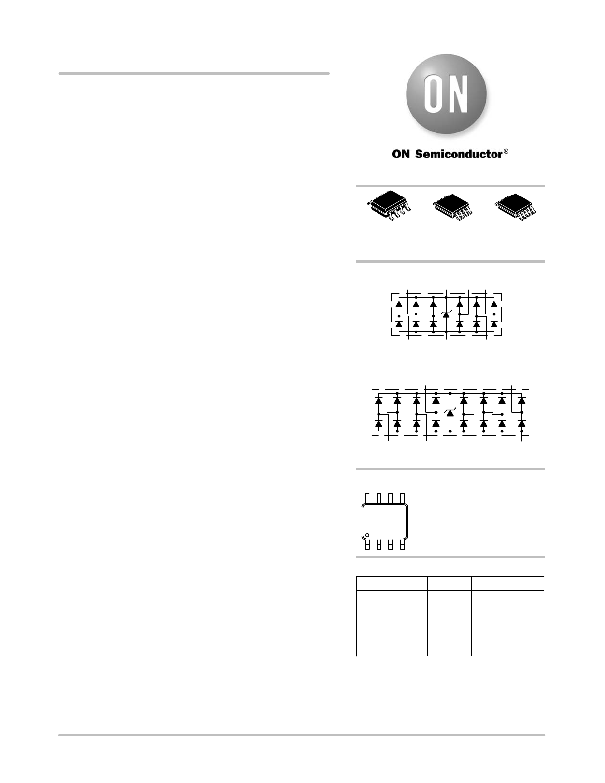
The CM1216 family of diode arrays provide sESD protection for
electronic components or sub−systems requiring minimal capacitive
loading. These devices are ideal for protecting systems with high data
and clock rates or for circuits requiring low capacitive loading. Each
ESD channel consists of a pair of diodes in series which steer the
positive or negative ESD current pulse to either the positive (V
negative (V
up to
N) supply rail. The CM1216 protects against ESD pulses
±15 kV per the IEC 61000−4−2 standard.
This device is particularly well−suited for protecting systems using
high−speed ports such as USB2.0, IEEE1394 (Firewire
Serial ATA, DVI, HDMI and corresponding ports in removable
storage, digital camcorders, DVD−RW drives and other applications
where extremely low loading capacitance with ESD protection are
required in a small package footprint.
Features
• Six and Eight Channels of ESD Protection
• Provides ±15 kV ESD Protection on Each Channel per the
IEC 61000−4−2 ESD Requirements
• Channel Loading Capacitance of 1.6 pF Typical
• Channel I/O to GND Capacitance Difference of 0.04 pF Typical
• Mutual Capacitance of 0.13 pF Typical
• Minimal Capacitance Change with Temperature and Voltage
• Each I/O Pin Can Withstand Over 1000 ESD Strikes
• SOIC and MSOP Packages
• These Devices are Pb−Free and are RoHS Compliant
Applications
• IEEE1394 Firewire
®
Ports at 400 Mbps / 800 Mbps
• DVI Ports, HDMI Ports in Notebooks, Set Top Boxes, Digital TVs,
LCD Displays
• Serial ATA Ports in Desktop PCs and Hard Disk Drives
• PCI Express Ports
• General Purpose High−Speed Data Line ESD Protection
®
, iLinkt),
P) or
http://onsemi.com
SOIC−8
SM SUFFIX
CASE 751AC
CH6 V
CH1 CH2 CH3
CH8 V
MARKING DIAGRAM
XXXXX
AYWWG
G
ORDERING INFORMATION
Device Package Shipping
CM1216−06SM SOIC
†For information on tape and reel specifications,
including part orientation and tape sizes, please
refer to our Tape and Reel Packaging Specification
Brochure, BRD8011/D.
MSOP−8
MR SUFFIX
CASE 846AD
BLOCK DIAGRAM
CH5 CH4
P
V
N
CM1216−06SM
CM1216−06MR
CH7 CH6 CH5
CH2CH1 CH4CH3
XXXXXX = Specific Device Code
A = Assembly Location
Y = Year
WW = Work Week
G = Pb−Free Package
P
CM1216−08MR
(Pb−Free)
MSOP
(Pb−Free)
MSOP
(Pb−Free)
MSOP−10
MR SUFFIX
CASE 846AE
2500/Tape & Reel
4000/Tape & ReelCM1216−06MR
4000/Tape & ReelCM1216−08MR
V
†
N
© Semiconductor Components Industries, LLC, 2011
February, 2011 − Rev. 3
1 Publication Order Number:
CM1216/D

CM1216
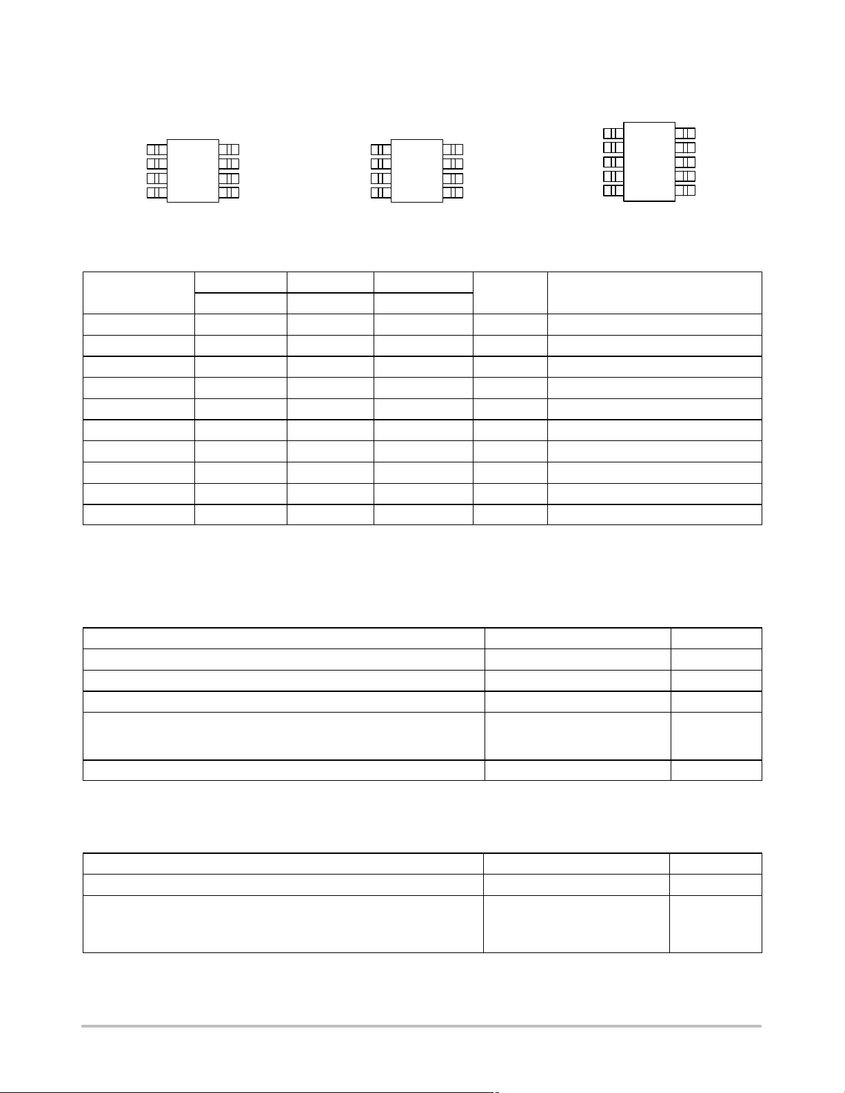
PACKAGE / PINOUT DIAGRAMS
Top View
CH1
CH2
V
CH3
1
E166
2
3
N
4
CH6
8
7
V
P
CH5
6
CH4
5
CH1
CH2
V
CH3
8−Pin SOIC−8
Table 1. PIN DESCRIPTIONS
Pin Name
CH1 1 1 1 I/O ESD Channel
CH2 2 2 2 I/O ESD Channel
CH3 4 4 3 I/O ESD Channel
CH4 5 5 4 I/O ESD Channel
V
N
CH5 6 6 6 I/O ESD Channel
CH6 8 8 7 I/O ESD Channel
V
P
CH7 − − 9 I/O ESD Channel
CH8 − − 10 I/O ESD Channel
MSOP−8 SOIC−8 MSOP−10
Pin No. Pin No. Pin No.
3 3 5 GND Negative voltage supply rail
7 7 8 PWR Positive voltage supply rail
Top View
1
2
3
N
4
8−Pin MSOP−8
E166
CH1
CH6
8
7
V
P
CH5
6
CH4
5
CH2
CH3
CH4
V
N
Type Description
Top View
1
10
E168
2
9
3
8
4
7
10−Pin MSOP−10
CH8
CH7
V
P
CH6
CH556
SPECIFICATIONS
Table 2. ABSOLUTE MAXIMUM RATINGS
Parameter Rating Units
Operating Supply Voltage (VP−VN) 6 V
Diode Forward DC Current 20
DC Voltage at any Channel Input (VN−0.5) to (VP+0.5) V
Operating Temperature Range
Ambient
Junction
−40 to +85
−40 to +125
Storage Temperature Range −40 to +150 °C
Stresses exceeding Maximum Ratings may damage the device. Maximum Ratings are stress ratings only. Functional operation above the
Recommended Operating Conditions is not implied. Extended exposure to stresses above the Recommended Operating Conditions may affect
device reliability.
Table 3. STANDARD OPERATING CONDITIONS
Parameter Rating Units
Temperature Range (Ambient) −40 to +85 °C
Package Power Rating
MSOP8 Package (CM1216−06MR)
SOIC8 Package (CM1216−06SM)
MSOP10 Package (CM1216−08MR)
400
600
400
mA
°C
mW
http://onsemi.com
2

CM1216
Table 4. ELECTRICAL OPERATING CHARACTERISTICS (Note 1)
Symbol
V
I
V
I
LEAK
C
DC
C
MUTUAL
V
ESD
V
CL
R
DYN
1. All parameters specified at TA = −40°C to +85°C unless otherwise noted.
2. Standard IEC 61000−4−2 with C
3. From I/O pins to V
Parameter
Operating Supply Voltage
P
(V
)
P−VN
Operating Supply Current (VP−VN) = 3.3 V 8
P
Diode Forward Voltage
F
Top Diode
IF = 20 mA; T
Bottom Diode
Channel Leakage Current T
Channel Input Capacitance At 1 MHz, V
IN
Channel Input Capacitance Matching 0.04 pF
IN
= 25°C; V
A
(Note 2)
Mutual Capacitance (VP−VN) = 3.3 V 0.13 pF
ESD Protection
Peak Discharge Voltage at any
T
= 25°C
A
(Notes 2 and 3)
channel input, in system,
contact discharge per
IEC 61000−4−2 standard
Channel Clamp Voltage
Positive Transients
I
PP
= 1 A, t
Negative Transients
Dynamic Resistance
Positive transients
I
PP
= 1 A, t
Negative transients
or V
only. VP bypassed to V
P
N
Discharge
= 150 pF, R
N
with low ESR 0.2 mF ceramic capacitor.
= 330 W, VP = 3.3 V, VN grounded.
Discharge
A
P
= 3.3 V, V
P
= 8/20 mS; T
P
= 8/20 mS; T
P
Conditions
= 25°C
= 5 V, V
Min Typ Max Units
3.3 5.5 V
0.6
0.8
0.6
0.8
= 0 V ±0.1 ±1.0
N
= 0 V, V
N
= 1.65 V
IN
1.6 2.0 pF
±15
= 25°C
A
+9.0
−1.5
= 25°C
A
0.6
0.4
mA
V
0.95
0.95
mA
kV
V
W
PERFORMANCE CHARACTERISTICS
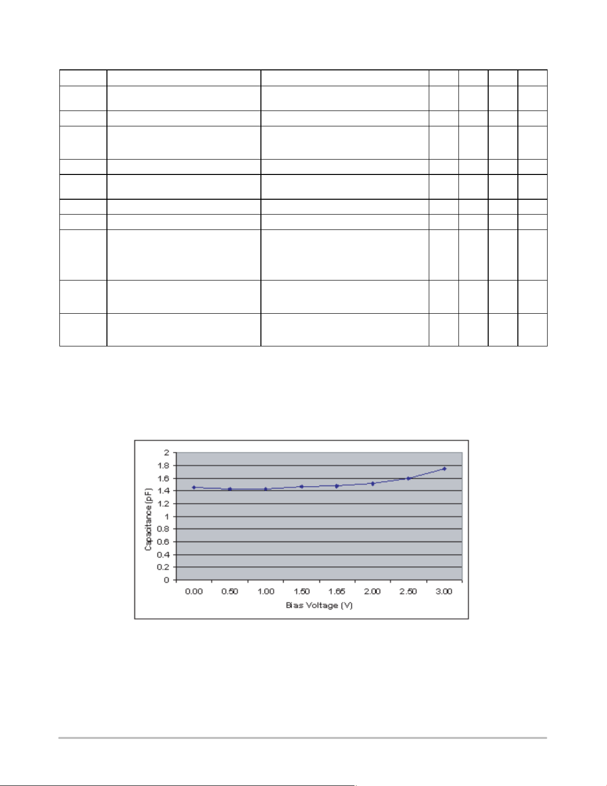
Figure 1. Typical Variation of CIN vs. V
(f = 1 MHz, VP= 3.3 V, VN = 0 V, 0.1 mF Chip Capacitor between VP and VN, TA = 255C)
IN
http://onsemi.com
3
 Loading...