

CAX803, CAX809, CAX810
3-Pin Microprocessor
Power Supply Supervisors
Description
The CAX803, CAX809, and CAX810 are supervisory circuits that
monitor power supplies in digital systems. The CAX803, CAX809,
and CAX810 are direct replacements for the MAX803, MAX809 and
MAX810 in applications operating over the industrial temperature range.
These devices generate a reset signal, which is asserted while the
power supply voltage is below a preset threshold level and for at least
140 ms after the power supply level has risen above that level. The
underlying floating gate technology, Analog EEPROM used by
ON Semiconductor, makes it possible to offer any custom reset
threshold value. Seven industry standard threshold levels are offered
to support +5.0 V, +3.3 V, +3.0 V and +2.5 V systems.
The CAX803 has an open−drain RESET
CAX803 requires a pull−up resistor on the reset output.
The CAX809 features a push−pull RESET
the CAX810 features a push−pull RESET output (active HIGH).
Fast transients on the power supply are ignored and the output is
guaranteed to be in the correct state at V
The CAX803, CAX809, and CAX810 are available in the compact
3−pin SOT−23 package.
Features
• Precision Monitoring of
+5.0 V (−5%, −10%, −20%),
+3.3 V (−5%, −10%),
+3.0 V (−10%) and
+2.5 V (−5%) Power Supplies
• Offered in Three Output Configurations:
− CAX803: Open−Drain Active LOW Reset
− CAX809: Push−Pull Active LOW Reset
− CAX810: Push−Pull Active HIGH Reset
• Direct Replacements for the MAX803, MAX809 and MAX810 in
Applications Operating over the Industrial Temperature Range
• Reset Valid down to V
= 1.0 V
CC
• 10 mA Power Supply Current
• Power Supply Transient Immunity
• Industrial Temperature Range: −40°C to +85°C
• Available in SOT−23 Package
• These Devices are Pb−Free and are RoHS Compliant
Applications
• Computers, Servers, Laptops, Cable Modems
• Wireless Communications
• Embedded Control Systems
• White Goods, Power Meters
• Intelligent Instruments
• PDAs and Handheld Equipment
output (active LOW). The
output (active LOW) and
levels as low as 1.0 V.
CC
http://onsemi.com
SOT−23
TB SUFFIX
CASE 527AG
PIN CONFIGURATION
1
GND
3
2
RESET
(RESET)
(Top View)
MARKING DIAGRAMS
XXXMG
G
SOT−23
XXX = Specific Device Code
M = Month Code
G = Pb−Free Package
(*Note: Microdot may be in either location)
ORDERING INFORMATION
See detailed ordering and shipping information in the package
dimensions section on page 9 of this data sheet.
3−Lead SOT23
V
CC
CAX803
CAX809
(CAX810)
© Semiconductor Components Industries, LLC, 2012
October, 2012 − Rev. 1
1 Publication Order Number:
CAX803/D
CAX803, CAX809, CAX810
Table 1. THRESHOLD SUFFIX SELECTOR
Nominal Threshold Voltage Threshold Suffix Designation
4.63 V L
4.55 V H
4.38 V M
4.00 V J
3.08 V T
2.93 V S
2.63 V R
2.32 V Z
Table 2. PIN DESCRIPTIONS
Pin Number
CAX803 CAX809 CAX810
1 1 1 GND Ground
2 2 − RESET Active LOW reset. RESET is asserted if VCC falls below the reset threshold and
− − 2 RESET Active HIGH reset. RESET is asserted if VCC falls below the reset threshold and
3 3 3 V
Name Description
CC
remains low for at least 140 ms after V
remains high for at least 140 ms after V
Power supply voltage that is monitored.
rises above the reset threshold.
CC
rises above the reset threshold.
CC
Table 3. ABSOLUTE MAXIMUM RATINGS
Parameter Rating Units
Any pin with respect to ground −0.3 to +6.0 V
Input Current, V
Output Current, RESET, RESET 20 mA
Rate of Rise, V
Continuous Power Dissipation
Derate 4 mW/°C above 70°C (SOT23)
Operating Temperature Range −40 to +85 °C
Storage Temperature Range −65 to +105 °C
Lead Soldering Temperature (10 sec) 300 °C
Stresses exceeding Maximum Ratings may damage the device. Maximum Ratings are stress ratings only. Functional operation above the
Recommended Operating Conditions is not implied. Extended exposure to stresses above the Recommended Operating Conditions may affect
device reliability.
CC
CC
20 mA
100
320
V/ms
mW
http://onsemi.com
2
CAX803, CAX809, CAX810
V
CC
V
V
CC
V
CC
CC
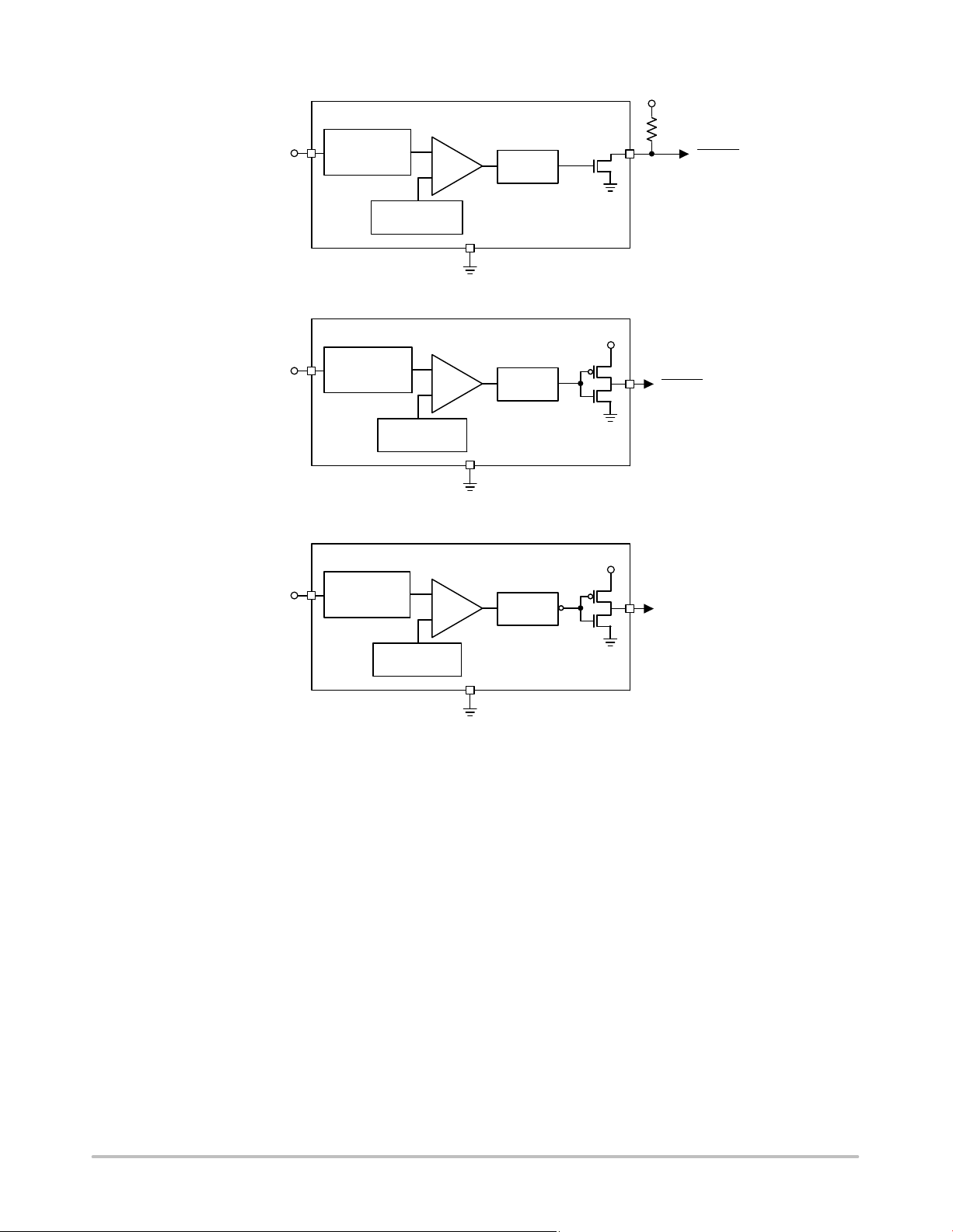
TOLERANCE
BIAS
VOLTAGE
REFERENCE
V
CC
TOLERANCE
BIAS
REFERENCE
+
–
+
–
VOLTAGE
GND
GND
DIGITAL
DELAY
DIGITAL
DELAY
CAX803
V
CC
CAX809
RESET
RESET
V
CC
V
V
CC
CC
TOLERANCE
BIAS
VOLTAGE
REFERENCE
+
–
DIGITAL
DELAY
RESET
CAX810
GND
Figure 1. Block Diagrams
http://onsemi.com
3

CAX803, CAX809, CAX810
Table 4. ELECTRICAL CHARACTERISTICS
(VCC = Full range, TA = −40°C to +85°C, unless otherwise specified. Typical values at TA = +25°C and VCC = 5 V for the L/H/M/J
versions, VCC = 3.3 V for the T/S versions, VCC = 3 V for the R version and VCC = 2.5 V for the Z/V versions.)
Typ
CC
CC
(Note 1)
Max Units
0.3
0.4
0.3
0.3
0.4
Symbol
VCC Range
Parameter Conditions Min
TA = 0°C to +70°C 1.0 5.5
TA = −40°C to +85°C 1.2 5.5
I
CC
V
TH
Supply Current TA = −40°C
to +85°C
Reset Threshold Voltage L Threshold
VCC < 5.5 V, J/L/M/H 15 25 mA
VCC < 3.6 V, R/S/T/Z/V 10 15
TA = +25°C 4.56 4.63 4.70
TA = −40°C to +85°C 4.50 4.75
H Threshold
TA = +25°C 4.48 4.55 4.62
TA = −40°C to +85°C 4.43 4.67
M Threshold
TA = +25°C 4.31 4.38 4.45
TA = −40°C to +85°C 4.25 4.50
J Threshold
TA = +25°C 3.93 4.00 4.06
TA = −40°C to +85°C 3.89 4.10
T Threshold
TA = +25°C 3.04 3.08 3.11
TA = −40°C to +85°C 3.00 3.15
S Threshold
TA = +25°C 2.89 2.93 2.96
TA = −40°C to +85°C 2.85 3.00
R Threshold
TA = +25°C 2.59 2.63 2.66
TA = −40°C to +85°C 2.55 2.70
Z Threshold
TA = +25°C 2.28 2.32 2.35
TA = −40°C to +85°C 2.25 2.38
Reset Threshold Tempco 30 ppm/°C
T
D
T
R
V
OL
V
OH
V
OL
V
OH
VCC to Reset Delay (Note 2) VCC = VTH to (VTH − 100 mV) 20
Reset Active Timeout Period TA = −40°C to +85°C 140 240 460 ms
RESET Output Voltage Low
(Open−drain active LOW,
CAX803 and push−pull,
active LOW, CAX809)
RESET Output Voltage High
(Push−pull, active LOW,
CAX809)
RESET Output Voltage Low
(Push−pull, active HIGH,
CAX810)
RESET Output Voltage High
(Push−pull, active HIGH,
CAX810)
VCC = VTH min, I
CAX803R/S/T/Z, CAX809R/S/T/Z/V
VCC = VTH min, I
CAX803J/L/M, CAX809J/L/M/H
VCC > 1.0 V, I
VCC = VTH max, I
CAX809R/S/T/Z/V
VCC = VTH max, I
CAX809J/L/M/H
VCC > VTH max, I
CAX810R/S/T/Z
VCC > VTH max, I
CAX810J/L/M
SINK
= 1.2 mA
SINK
= 3.2 mA
SINK
= 50 mA
SOURCE
SOURCE
= 1.2 mA
SINK
= 3.2 mA
SINK
= 500 mA
= 800 mA
1.8 V < VCC VTH min,
SOURCE
= 150 mA
I
1. Production testing done at TA = +25°C; limits over temperature guaranteed by design only.
2. RESET
output for the CAX809; RESET output for the CAX810.
0.8 V
VCC − 1.5
0.8 V
V
V
ms
V
V
V
V
http://onsemi.com
4

CAX803, CAX809, CAX810
(VCC = Full range, TA = −40°C to +85°C, unless otherwise specified. Typical values at TA = +25°C and VCC = 5 V for the
TYPICAL OPERATING CHARACTERISTICS
L/M/J versions, V
260
240
220
200
180
POWER−UP RESET TIMEOUT (mS)
160
Figure 2. Power−up Reset Timeout vs.
14
12
= 3.3 V for the T/S versions, VCC = 3 V for the R version and VCC = 2.5 V for the Z version.)
CC
1.9
VCC = 5 V
VCC = 2.5 V
150100500−50
TEMPERATURE (°C) TEMPERATURE (°C)
1.6
1.3
1.0
0.7
0.4
NORMALIZED SUPPLY CURRENT (mA)
0
Figure 3. Supply Current vs. Temperature
Temperature
1.0002
1.0000
(No Load, CAX8xxR/S/T/Z)
100500−50
150
10
8
6
4
2
POWER−DOWN RESET DELAY (mS)
0
TEMPERATURE (°C) TEMPERATURE (°C)
Figure 4. Power−down Reset Delay vs.
Temperature (CAX8xxR/S/T/Z)
0.9998
0.9996
0.9994
0.9992
NORMALIZED THRESHOLD
0.9990
0.9988
150100500−50
Figure 5. Normalized Reset Threshold vs.
120100806040200
Temperature
http://onsemi.com
5

CAX803, CAX809, CAX810
Detailed Descriptions
Reset Timing
The reset signal is asserted LOW for the CAX803/CAX809 and HIGH for the CAX810 when the power supply voltage falls
below the threshold trip voltage and remains asserted for at least 140 ms after the power supply voltage has risen above the
threshold.
5 V
V
TH
V
CC
0 V
T
R
(140 ms
minimum)
Reset Timeout Period
CAX803, CAX809
CAX810
5 V
RESET/OUT
0 V
5 V
RESET
T
D
0 V
Figure 6. Reset Timing Diagram
VCC Transient Response
The CAX803/CAX809/CAX810 protect mPs against
brownout failure. Short duration transients of 4 msec or less
and 100 mV amplitude typically do not cause a false RESET.
Figure 7 shows the maximum pulse duration of negative−
going V
transients that do not cause a reset condition.
CC
As the amplitude of the transient goes further below the
threshold (increasing V
duration decreases. In this test, the V
− VCC), the maximum pulse
TH
starts from an initial
CC
voltage of 0.5 V above the threshold and drops below it by
the amplitude of the overdrive voltage (V
− VCC).
TH
30
T
AMB
25
20
15
CAX809Z
10
CAX809M
5
TRANSIENT DURATION (ms)
0
RESET OVERDRIVE VTH − VCC (mV)
Figure 7. Maximum Transient Duration without
Causing a Reset Pulse vs. Reset Comparator
Overdrive
= 25°C
1000100101
http://onsemi.com
6

CAX803, CAX809, CAX810
Valid RESET with VCC Under 1.0 V
To ensure that the CAX809 RESET pin is in a known state when VCC is under 1.0 V, a >10 kW pull−down resistor between
RESET
pin and GND is recommended. For the CAX810, a pull−up resistor from RESET pin to VCC is needed.
Power
Supply
V
CC
CAX809
RESET
GND
10 kW
Power
Supply
V
CC
CAX810
RESET
GND
10 kW
Figure 8. RESET Valid with VCC Under 1.0 V Figure 9. RESET Valid with VCC Under 1.1 V
Bi−directional Reset Pin Interfacing
The CAX809/810 can interface with mP/mC bi−directional reset pins by connecting a 4.7 kW resistor in series with the
CAX809/810 reset output and the mP/mC bi−directional reset pin.
Power
Supply
BUF
V
CC
Buffered
RESET
CAX809
RESET
GND
4.7 kW
Bi−directional
I/O Pin
Figure 10. Bi−directional Reset Pin Interfacing
CAX803 Open−Drain RESET Application
The CAX803 features an open−drain RESET output and
therefore needs a pull−up resistor on the output for proper
operation, as shown on Figure 11. An advantage of the
open−drain output includes the ability to “wire AND”
several outputs together to form an inexpensive logic circuit.
It is also possible to have the pull−up resistor connected to
a different supply which can be higher than the CAX803
V
pin. The value of the pull−up resistor is not critical in
CC
most applications, typical values being between 5 kW and
10 kW.
V
CC
mP
RESET
INPUT
GND
Power
Supply
(For example:
68HC11)
V
CC
CAX803
RESET
GND
Figure 11. Typical CAX803 Open−Drain
Circuit Configuration
5 kW
RESET
INPUT
V
CC
mP
GND
http://onsemi.com
7

CAX803, CAX809, CAX810
PACKAGE DIMENSIONS
SOT−23, 3 Lead
CASE 527AG−01
ISSUE O
D
3
E1 E
12
e
e1
TOP VIEW
A
b
A1
SYMBOL
A
A1
b
c
D
E
E1
e
e1
L
L1
θ
q
MIN NOM MAX
0.89
0.013
0.37
0.085
2.80
2.10
1.20
0.95 BSC
1.90 BSC
0.40 REF
0.54 REF
0º 8º
L1 L
1.12
0.10
0.50
0.18
3.04
2.64
1.40
c
SIDE VIEW END VIEW
Notes:
(1) All dimensions are in millimeters. Angles in degrees.
(2) Complies with JEDEC TO-236.
http://onsemi.com
8

CAX803, CAX809, CAX810
Table 5. ORDERING PART NUMBER
Top Mark
Order Number Voltage
(Note 3)
Output Reset Package
CAX803LTBI−T3 4.63 V
CAX803MTBI−T3 4.38 V
CAX803JTBI−T3 4.00 V
CAX803TTBI−T3 3.08 V
VKL
Open
Drain
LOW SOT−23−3 3,000
CAX803STBI−T3 2.93 V
CAX803RTBI−T3 2.63 V
CAX803ZTBI−T3 2.32 V
CAX809LTBI−T3 4.63 V
CAX809HTBI−T3 4.55 V
CAX809MTBI−T3 4.38 V
CAX809JTBI−T3 4.00 V
CAX809TTBI−T3 3.08 V
VLD
CMOS /
Push−Pull
LOW SOT−23−3 3,000
CAX809STBI−T3 2.93 V
CAX809RTBI−T3 2.63 V
CAX809ZTBI−T3 2.32 V
CAX810LTBI−T3 4.63 V
CAX810MTBI−T3 4.38 V
CAX810JTBI−T3 4.00 V
CAX810TTBI−T3 3.08 V
VHT
CMOS /
Push−Pull
HIGH SOT−23−3 3,000
CAX810STBI−T3 2.93 V
CAX810RTBI−T3 2.63 V
CAX810ZTBI−T3 2.32 V
3. Threshold and full part numbers will be provided on box and reel labels as well as all Shipping documents.
4. For information on tape and reel specifications, including part orientation and tape sizes, please refer to our Tape and Reel Packaging
Specifications Brochure, BRD8011/D.
5. For detailed information and a breakdown of device nomenclature and numbering systems, please see the ON Semiconductor Device
Nomenclature document, TND310/D, available at www.onsemi.com
Quantity per Reel
(Note 4)
ON Semiconductor and are registered trademarks of Semiconductor Components Industries, LLC (SCILLC). SCILLC owns the rights to a number of patents, trademarks,
copyrights, trade secrets, and other intellectual property. A listing of SCILLC’s product/patent coverage may be accessed at www.onsemi.com/site/pdf/Patent−Marking.pdf. SCILLC
reserves the right to make changes without further notice to any products herein. SCILLC makes no warranty, representation or guarantee regarding the suitability of its products for any
particular purpose, nor does SCILLC assume any liability arising out of the application or use of any product or circuit, and specifically disclaims any and all liability, including without
limitation special, consequential or incidental damages. “Typical” parameters which may be provided in SCILLC data sheets and/or specifications can and do vary in different applications
and actual performance may vary over time. All operating parameters, including “Typicals” must be validated for each customer application by customer’s technical experts. SCILLC
does not convey any license under its patent rights nor the rights of others. SCILLC products are not designed, intended, or authorized for use as components in systems intended for
surgical implant into the body, or other applications intended to support or sustain life, or for any other application in which the failure of the SCILLC product could create a situation where
personal injury or death may occur. Should Buyer purchase or use SCILLC products for any such unintended or unauthorized application, Buyer shall indemnify and hold SCILLC and
its officers, employees, subsidiaries, affiliates, and distributors harmless against all claims, costs, damages, and expenses, and reasonable attorney fees arising out of, directly or indirectly,
any claim of personal injury or death associated with such unintended or unauthorized use, even if such claim alleges that SCILLC was negligent regarding the design or manufacture
of the part. SCILLC is an Equal Opportunity/Affirmative Action Employer. This literature is subject to all applicable copyright laws and is not for resale in any manner.
PUBLICATION ORDERING INFORMATION
LITERATURE FULFILLMENT:
Literature Distribution Center for ON Semiconductor
P.O. Box 5163, Denver, Colorado 80217 USA
Phone: 303−675−2175 or 800−344−3860 Toll Free USA/Canada
Fax: 303−675−2176 or 800−344−3867 Toll Free USA/Canada
Email: orderlit@onsemi.com
N. American Technical Support: 800−282−9855 Toll Free
USA/Canada
Europe, Middle East and Africa Technical Support:
Phone: 421 33 790 2910
Japan Customer Focus Center
Phone: 81−3−5817−1050
http://onsemi.com
ON Semiconductor Website: www.onsemi.com
Order Literature: http://www.onsemi.com/orderlit
For additional information, please contact your local
Sales Representative
CAX803/D
9

 Loading...