

Page 1
BAV99L, SBAV99L
s
l
l
Dual Series
Switching Diode
Features
• S Prefix for Automotive and Other Applications Requiring Unique
Site and Control Change Requirements; AEC−Q101 Qualified and
PPAP Capable
• These Devices are Pb−Free, Halogen Free/BFR Free and are RoHS
Compliant*
MAXIMUM RATINGS (Each Diode)
Rating
Reverse Voltage V
Forward Current I
Peak Forward Surge Current I
Repetitive Peak Reverse Voltage V
Average Rectified Forward Current (Note 1)
(averaged over any 20 ms period)
Repetitive Peak Forward Current I
Non−Repetitive Peak Forward Current
t = 1.0 ms
t = 1.0 ms
t = 1.0 s
Stresses exceeding those listed in the Maximum Ratings table may damage
the device. If any of these limits are exceeded, device functionality should not
be assumed, damage may occur and reliability may be affected.
THERMAL CHARACTERISTICS
Characteristic Symbol Max Unit
Total Device Dissipation
FR−5 Board (Note 1) TA = 25°C
Derate above 25°C
Thermal Resistance, Junction−to−Ambient
Total Device Dissipation
Alumina Substrate (Note 2)
T
= 25°C
A
Derate above 25°C
Thermal Resistance, Junction−to−Ambient
Junction and Storage
Temperature Range
1. FR−5 = 1.0 0.75 0.062 in.
2. Alumina = 0.4 0.3 0.024 in 99.5% alumina.
*For additional information on our Pb−Free strategy and soldering details, please
download the ON Semiconductor Soldering and Mounting Techniques
Reference Manual, SOLDERRM/D.
Symbol Value Unit
stg
100 Vdc
215 mAdc
500 mAdc
100 V
715 mA
450 mA
2.0
1.0
0.5
225
1.8mWmW/°C
556 °C/W
300
2.4mWmW/°C
417 °C/W
−65 to
+150
A
°C
R
F
FM(surge)
RRM
I
F(AV)
FRM
I
FSM
P
D
R
q
JA
P
D
R
q
JA
TJ, T
www.onsemi.com
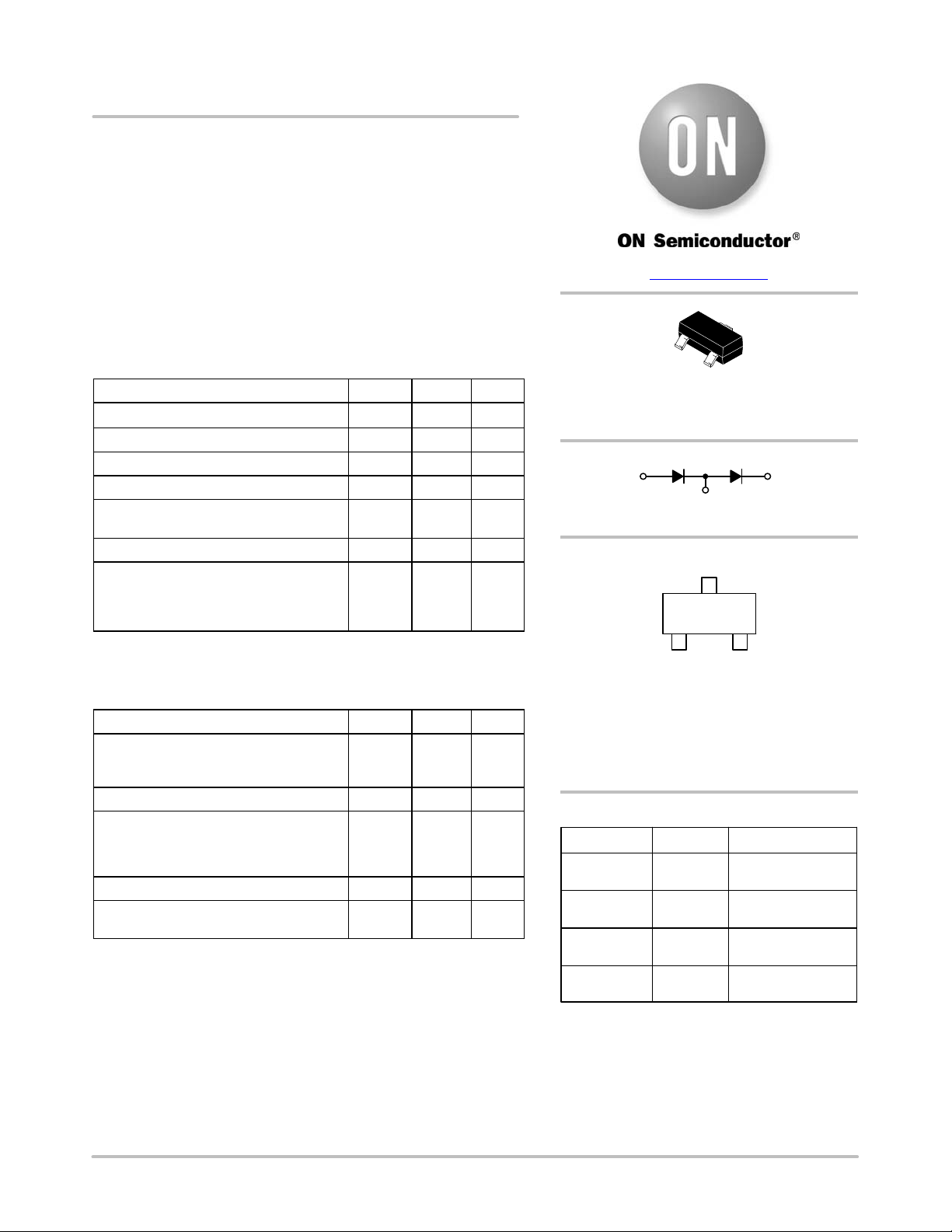
CASE 318
SOT−23
STYLE 11
ANODE
1
3
CATHODE/ANODE
CATHODE
2
MARKING DIAGRAM
A7 MG
G
1
A7 = Device Code
M = Date Code*
G = Pb−Free Package
(Note: Microdot may be in either location)
*Date Code orientation and/or overbar may
vary depending upon manufacturing location.
ORDERING INFORMATION
Device Package Shipping
BAV99LT1G SOT−23
(Pb−Free)
SBAV99LT1G SOT−23
(Pb−Free)
BAV99LT3G SOT−23
(Pb−Free)
SBAV99LT3G SOT−23
(Pb−Free)
†For information on tape and reel specifications,
including part orientation and tape sizes, please
refer to our Tape and Reel Packaging Specification
Brochure, BRD801 1/D.
3,000 / Tape & Reel
3,000 / Tape & Reel
10,000 / Tape & Ree
10,000 / Tape & Ree
†
© Semiconductor Components Industries, LLC, 2015
December, 2015 − Rev. 11
1 Publication Order Number:
BAV99LT1/D
Page 2
BAV99L, SBAV99L
OFF CHARACTERISTICS (T
= 25°C unless otherwise noted) (Each Diode)
A
Characteristic
Reverse Breakdown Voltage,
= 100 mA)
(I
(BR)
Reverse Voltage Leakage Current,
(V
= 100 Vdc)
R
= 25 Vdc, TJ = 150°C)
(V
R
(VR = 70 Vdc, TJ = 150°C)
Diode Capacitance,
(V
= 0, f = 1.0 MHz)
R
Forward Voltage,
(I
= 1.0 mAdc)
F
(IF = 10 mAdc)
= 50 mAdc)
(I
F
(I
= 150 mAdc)
F
Reverse Recovery Time,
= IR = 10 mAdc, i
(I
F
= 1.0 mAdc) RL = 100 W
R(REC)
Forward Recovery Voltage,
(I
= 10 mA, t
F
= 20 ns)
r
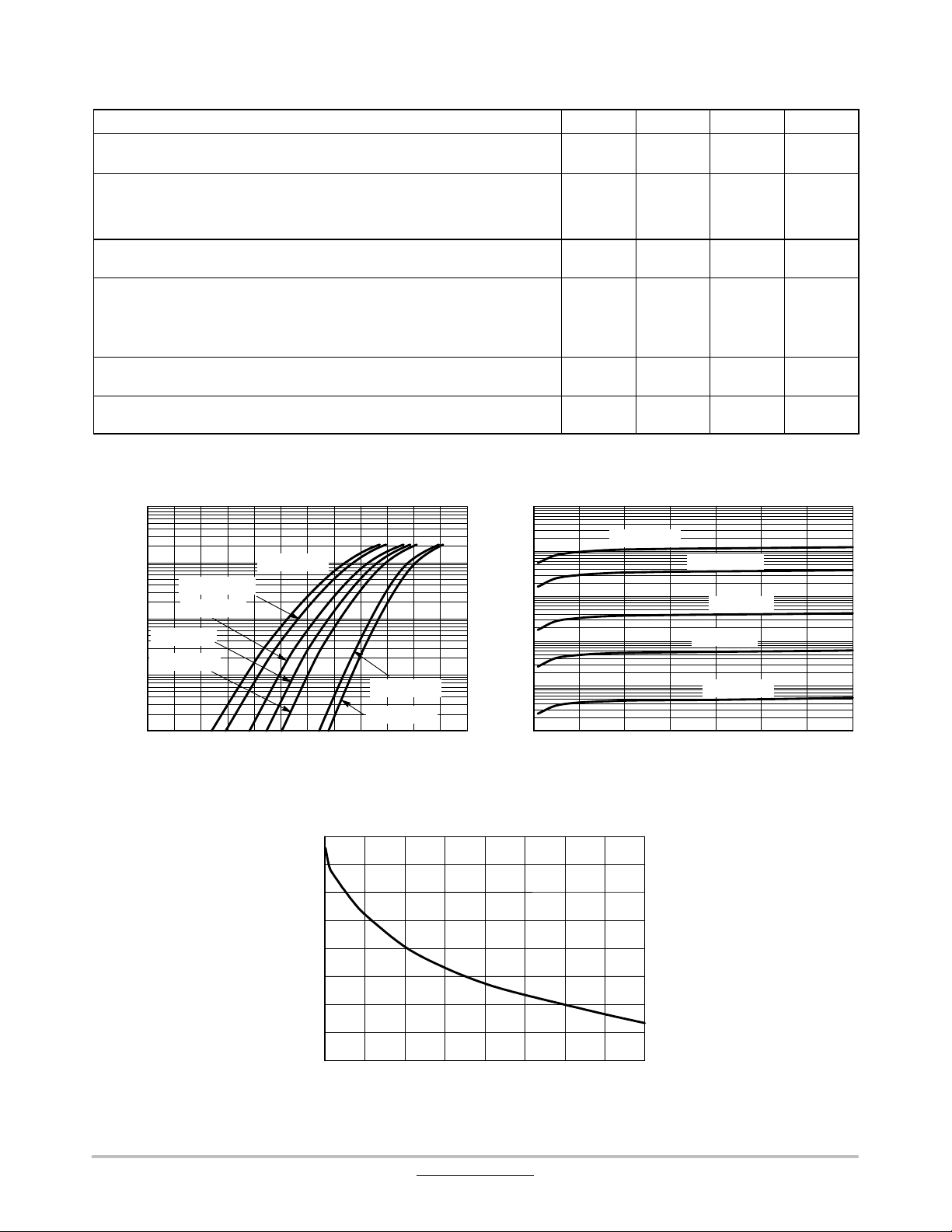
CURVES APPLICABLE TO EACH DIODE
1000
100
TA = 125°C
10
TA = 85°C
TA = 55°C
TA = 25°C
1
, FORWARD CURRENT (mA)
F
I
0.1
0 1.1 1.2
0.1 0.2 0.3 0.4 0.5 0.6 0.7 0.8 0.9 1.0
TA = 150°C
TA = −55°C
VF, FORWARD VOLTAGE (V) VR, REVERSE VOLTAGE (V)
Figure 1. Forward Voltage Figure 2. Leakage Current
TA = −40°C
Symbol Min Max Unit
V
V
(BR)
I
R
C
V
t
rr
FR
D
F
100 −
−
−
−
− 1.5
−
−
−
−
715
855
1000
1250
− 6.0
− 1.75
1.0
30
50
100
10
TA = 150°C
TA = 125°C
1.0
0.1
0.01
, REVERSE CURRENT (mA)
R
I
TA = 85°C
TA = 55°C
TA = 25°C
0.001
0 10203040506070
Vdc
mAdc
pF
mVdc
ns
V
0.61
0.59
0.57
0.55
0.53
0.51
0.49
, DIODE CAPACITANCE (pF)
d
0.47
C
0.45
012345678
, REVERSE VOLTAGE (V)
V
R
Figure 3. Capacitance
www.onsemi.com
2
Page 3

BAV99L, SBAV99L
P
al
PACKAGE DIMENSIONS
SOT−23 (TO−236)
CASE 318−08
ISSUE AP
NOTES:
1. DIMENSIONING AND TOLERANCING PER ANSI Y14.5M,
D
H
SEE VIEW C
E
c
0.25
3
E
12
b
e
q
A
L
A1
L1
VIEW C
1982.
2. CONTROLLING DIMENSION: INCH.
3. MAXIMUM LEAD THICKNESS INCLUDES LEAD FINISH
THICKNESS. MINIMUM LEAD THICKNESS IS THE MINIMUM
THICKNESS OF BASE MATERIAL.
4. DIMENSIONS D AND E DO NOT INCLUDE MOLD FLASH,
PROTRUSIONS, OR GATE BURRS.
DIMAMIN NOM MAX MIN
A1 0.01 0.06 0.10 0.001
b 0.37 0.44 0.50 0.015
c 0.09 0.13 0.18 0.003
D 2.80 2.90 3.04 0.110
E 1.20 1.30 1.40 0.047
e 1.78 1.90 2.04 0.070
L 0.10 0.20 0.30 0.004
L1
H
q
STYLE 11:
PIN 1. ANODE
MILLIMETERS
0.89 1.00 1.11 0.035
0.35 0.54 0.69 0.014 0.021 0.029
2.10 2.40 2.64 0.083 0.094 0.104
E
0 −−− 10 0 −−− 10
2. CATHODE
3. CATHODE−ANODE
INCHES
NOM MAX
0.040 0.044
0.002 0.004
0.018 0.020
0.005 0.007
0.114 0.120
0.051 0.055
0.075 0.081
0.008 0.012
°°°°
SOLDERING FOOTPRINT
0.95
0.95
0.037
0.9
0.035
0.8
0.031
ON Semiconductor and are registered trademarks of Semiconductor Components Industries, LLC (SCILLC). SCILLC owns the rights to a number of patents, trademarks,
copyrights, trade secrets, and other intellectual property. A listing of SCILLC’s product/patent coverage may be accessed at www.onsemi.com/site/pdf/Patent−Marking.pdf. SCILLC
reserves the right to m ake c hanges w ithout f urt her n otice t o a ny p roducts h erein. SCILLC makes no warranty, representation or guarantee regarding the s uitability o f i ts p roducts f or a ny
particular purpose, nor does SCILLC assume any liability arising out of the application or use of any product or circuit, and specifically disclaims any and all liability, including without
limitation special, consequent ial o r i ncidental d amages. “ Typical” parameters which m ay b e p rovided i n S CILLC d at a s heets and/or specifications can a nd d o v ary i n d iff erent applications
and actual performance may vary over time. All operating parameters, including “Typicals” must be validated for each customer application by customer’s technical experts. SCILLC
does not convey any license under its patent rights nor the rights of others. SCILLC products are not designed, intended, or authorized for use as components in systems intended for
surgical implant into t he b ody, or other a pplications i ntended t o s upport or sustain life, or f or a ny o ther a pplication i n w hich the failure of the SCILLC p roduct c ould creat e a s ituat ion w here
personal injury or death may occur. S hould B uyer p urchase o r u se S CILLC p r oduct s for any such unintended or unauthorized application, Buyer shall indemnify and hold SCILLC and
its officers, e mployees, s ubsidiaries, a ffiliat es, a nd d istributor s h arm less a gainst a ll c laims, c osts, d amages, a nd e xpenses, and r easonable a ttorney f ees a rising o ut o f, d irectly o r i ndirectly,
any claim of personal injury or death associated with such unintended or unauthorized use, even if such claim a lleges t hat SCILLC was negligent regarding the design or manufacture
of the part. SCILLC is an Equal Opportunity/Affirmative Action Employer. This literature is subject to all applicable copyright laws and is not for resale in any manner.
0.037
SCALE 10:1
2.0
0.079
ǒ
inches
mm
Ǔ
UBLICATION ORDERING INFORMATION
LITERATURE FULFILLMENT:
Literature Distribution Center for ON Semiconductor
P.O. Box 5163, Denver, Colorado 80217 USA
Phone: 303−675−2175 or 800−344−3860 Toll Free USA/Canada
Fax: 303−675−2176 or 800−344−3867 Toll Free USA/Canada
Email: orderlit@onsemi.com
N. American Technical Support: 800−282−9855 Toll Free
USA/Canada
Europe, Middle East and Africa Technical Support:
Phone: 421 33 790 2910
Japan Customer Focus Center
Phone: 81−3−5817−1050
www.onsemi.com
ON Semiconductor Website: www.onsemi.com
Order Literature: http://www.onsemi.com/orderlit
For additional information, please contact your loc
Sales Representative
BAV99LT1/D
3
Page 4

 Loading...