

BAT54HT1G,
NSVBAT54HT1G
Schottky Barrier Diodes
These Schottky barrier diodes are designed for high speed switching
applications, circuit protection, and voltage clamping. Extremely low
forward voltage reduces conduction loss. Miniature surface mount
package is excellent for hand held and portable applications where
space is limited.
Features
Extremely Fast Switching Speed
Low Forward Voltage − 0.35 V (Typ) @ I
Device Marking: JV
AEC Qualified and PPAP Capable
NSV Prefix for Automotive and Other Applications Requiring
Unique Site and Control Change Requirements
These Devices are Pb−Free, Halogen Free/BFR Free and are RoHS
Compliant*
= 10 mAdc
F
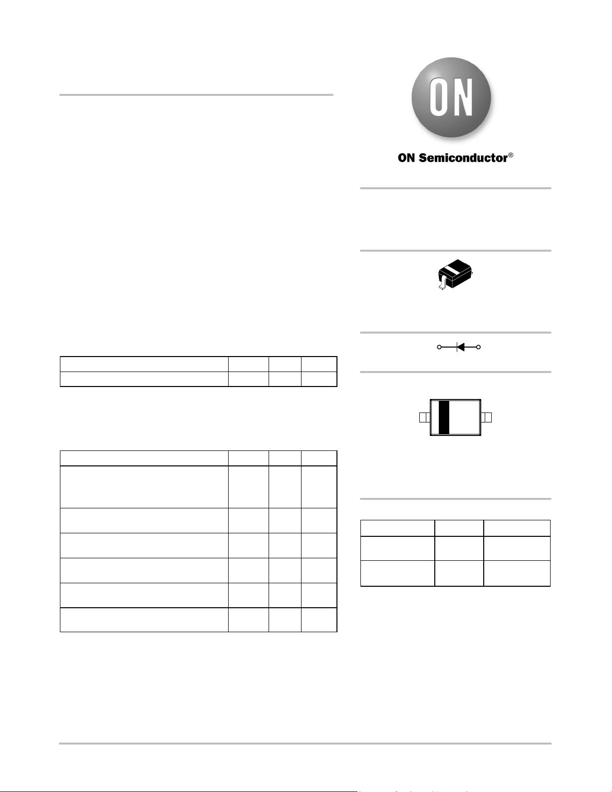
http://onsemi.com
30 VOLT SILICON
HOT−CARRIER DETECTOR
AND SWITCHING DIODES
SOD−323
CASE 477
STYLE 1
MAXIMUM RATINGS (T
Reverse Voltage V
Stresses exceeding Maximum Ratings may damage the device. Maximum
Ratings are stress ratings only. Functional operation above the Recommended
Operating Conditions is not implied. Extended exposure to stresses above the
Recommended Operating Conditions may affect device reliability.
= 125C unless otherwise noted)
J
Rating
Symbol Value Unit
R
30 V
THERMAL CHARACTERISTICS
Characteristic Symbol Max Unit
Total Device Dissipation FR−5 Board,
(Note 1)
T
= 25C
A
Derate above 25C
Forward Current (DC) I
Non−Repetitive Peak Forward Current,
t
< 10 msec
p
Repetitive Peak Forward Current
Pulse Wave = 1 sec, Duty Cycle = 66%
Thermal Resistance
Junction−to−Ambient
Junction and Storage Temperature Range TJ, T
1. FR−4 Minimum Pad
P
I
FSM
I
FRM
R
D
200
1.57mWmW/C
F
q
200
Max
600
300
JA
635
−55
stg
to150
mA
mA
mA
C/W
C
1
CATHODE
2
ANODE
MARKING DIAGRAM
JVM G
G
1
JV = Device Code
M = Date Code
G = Pb−Free Package
(Note: Microdot may be in either location)
2
ORDERING INFORMATION
Device Package Shipping
BAT54HT1G SOD−323
NSVBAT54HT1G SOD−323
†For information on tape and reel specifications,
including part orientation and tape sizes, please
refer to our Tape and Reel Packaging Specifications
Brochure, BRD8011/D.
(Pb−Free)
(Pb−Free)
Tape & Reel
Tape & Reel
†
3,000 /
3,000 /
*For additional information on our Pb−Free strategy and soldering details, please
download the ON Semiconductor Soldering and Mounting Techniques
Reference Manual, SOLDERRM/D.
Semiconductor Components Industries, LLC, 2011
November, 2011 − Rev. 6
1 Publication Order Number:
BAT54HT1/D
BAT54HT1G, NSVBAT54HT1G
ELECTRICAL CHARACTERISTICS (T
Characteristic
Reverse Breakdown Voltage
(IR = 10 A)
Total Capacitance
(V
= 1.0 V, f = 1.0 MHz)
R
Reverse Leakage
(V
= 25 V)
R
Forward Voltage
(I
= 0.1 mAdc)
F
Forward Voltage
(I
= 30 mAdc)
F
Forward Voltage
(IF = 100 mAdc)
Reverse Recovery Time
(I
= IR = 10 mAdc, I
F
Forward Voltage
(I
= 1.0 mAdc)
F
Forward Voltage
(I
= 10 mAdc)
F
= 1.0 mAdc) Figure 1
R(REC)
= 25C unless otherwise noted)
A
Symbol Min Typ Max Unit
V
(BR)R
C
T
I
R
V
F
V
F
V
F
t
rr
V
F
V
F
30 − −
− 7.6 10
− 0.5 2.0
− 0.22 0.24
− 0.41 0.5
− 0.52 0.8
− − 5.0
− 0.29 0.32
− 0.35 0.40
V
pF
Adc
Vdc
Vdc
Vdc
ns
Vdc
Vdc
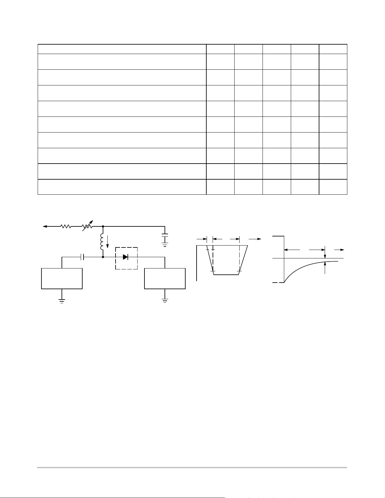
+10 V
50 Output
Generator
820
Pulse
2 k
0.1 F
100 H
I
0.1 F
F
t
t
r
p
t
I
F
10%
DUT
50 Input
Sampling
Oscilloscope
V
R
90%
INPUT SIGNAL
I
R
(I
Notes: 1. A 2.0 k variable resistor adjusted for a Forward Current (IF) of 10 mA.
Notes: 2. Input pulse is adjusted so I
Notes: 3. t
» t
p
rr
is equal to 10 mA.
R(peak)
Figure 1. Recovery Time Equivalent Test Circuit
t
rr
= 1 mA
i
R(REC)
OUTPUT PULSE
= IR = 10 mA; measured
F
at i
R(REC)
= 1 mA)
t
http://onsemi.com
2

100
BAT54HT1G, NSVBAT54HT1G
10
1.0
, FORWARD CURRENT (mA)
F
I
0.1
0.0 0.1
150C
125C
85C
VF, FORWARD VOLTAGE (VOLTS)
Figure 2. Forward Voltage
1000
TA = 150C
100
10
1.0
0.1
25C
0.2 0.3 0.4
−40C
−55C
0.5
TA = 125C
TA = 85C
0.6
, REVERSE CURRENT (A)
0.01
R
I
0.001
14
12
10
8
6
4
, TOATAL CAPACITANCE (pF)
2
T
C
0
TA = 25C
0
5101520
, REVERSE VOLTAGE (VOLTS)
V
R
25
30
Figure 3. Leakage Current
0
51015 30
V
, REVERSE VOLTAGE (VOLTS)
R
2520
Figure 4. Total Capacitance
http://onsemi.com
3

C
NOTE 3
1
L
NOTE 5
BAT54HT1G, NSVBAT54HT1G
PACKAGE DIMENSIONS
SOD−323
CASE 477−02
ISSUE H
NOTES:
1. DIMENSIONING AND TOLERANCING PER ANSI
H
E
D
E
2b
A3
A
A1
SOLDERING FOOTPRINT*
Y14.5M, 1982.
2. CONTROLLING DIMENSION: MILLIMETERS.
3. LEAD THICKNESS SPECIFIED PER L/F DRAWING
WITH SOLDER PLATING.
4. DIMENSIONS A AND B DO NOT INCLUDE MOLD
FLASH, PROTRUSIONS OR GATE BURRS.
5. DIMENSION L IS MEASURED FROM END OF RADIUS.
MILLIMETERS
DIM MIN NOM MAX
A 0.80 0.90 1.00
A1 0.00 0.05 0.10
A3 0.15 REF
b 0.25 0.32 0.4
C 0.089 0.12 0.177
D 1.60 1.70 1.80
E 1.15 1.25 1.35
0.08
L
H
2.30 2.50 2.70
E
STYLE 1:
PIN 1. CATHODE (POLARITY BAND)
2. ANODE
INCHES
MIN NOM MAX
0.031 0.035 0.040
0.000 0.002 0.004
0.006 REF
0.010 0.012 0.016
0.003 0.005 0.007
0.062 0.066 0.070
0.045 0.049 0.053
0.003
0.090 0.098 0.105
0.63
0.025
0.83
0.033
1.60
0.063
2.85
0.112
*For additional information on our Pb−Free strategy and soldering
details, please download the ON Semiconductor Soldering and
Mounting Techniques Reference Manual, SOLDERRM/D.
ON Semiconductor and are registered trademarks of Semiconductor Components Industries, LLC (SCILLC). SCILLC reserves the right to make changes without further notice
to any products herein. SCILLC makes no warranty, representation or guarantee regarding the suitability of its products for any particular purpose, nor does SCILLC assume any liability
arising out of the application or use of any product or circuit, and specifically disclaims any and all liability, including without limitation special, consequential or incidental damages.
“Typical” parameters which may be provided in SCILLC data sheets and/or specifications can and do vary in different applications and actual performance may vary over time. All
operating parameters, including “Typicals” must be validated for each customer application by customer’s technical experts. SCILLC does not convey any license under its patent rights
nor the rights of others. SCILLC products are not designed, intended, or authorized for use as components in systems intended for surgical implant into the body, or other applications
intended to support or sustain life, or for any other application in which the failure of the SCILLC product could create a situation where personal injury or death may occur. Should
Buyer purchase or use SCILLC products for any such unintended or unauthorized application, Buyer shall indemnify and hold SCILLC and its officers, employees, subsidiaries, affiliates,
and distributors harmless against all claims, costs, damages, and expenses, and reasonable attorney fees arising out of, directly or indirectly, any claim of personal injury or death
associated with such unintended or unauthorized use, even if such claim alleges that SCILLC was negligent regarding the design or manufacture of the part. SCILLC is an Equal
Opportunity/Affirmative Action Employer. This literature is subject to all applicable copyright laws and is not for resale in any manner.
PUBLICATION ORDERING INFORMATION
LITERATURE FULFILLMENT:
Literature Distribution Center for ON Semiconductor
P.O. Box 5163, Denver, Colorado 80217 USA
Phone: 303−675−2175 or 800−344−3860 Toll Free USA/Canada
Fax: 303−675−2176 or 800−344−3867 Toll Free USA/Canada
Email: orderlit@onsemi.com
N. American Technical Support: 800−282−9855 Toll Free
USA/Canada
Europe, Middle East and Africa Technical Support:
Phone: 421 33 790 2910
Japan Customer Focus Center
Phone: 81−3−5817−1050
http://onsemi.com
4
ON Semiconductor Website: www.onsemi.com
Order Literature: http://www.onsemi.com/orderlit
For additional information, please contact your local
Sales Representative
BAT54HT1/D

 Loading...