

ADM1032
+15C Remote and Local
System Temperature Monitor
The ADM1032 is a dual-channel digital thermometer and
under/overtemperature alarm intended for use in PCs and thermal
management systems. The device can measure the temperature of a
remote thermal diode, which can be located on the processor die or can
be a discrete device (2N3904/06), accurate to 1°C. A novel
measurement technique cancels out the absolute value of the
transistor’s base emitter voltage so that no calibration is required. The
ADM1032 also measures its ambient temperature.
The ADM1032 communicates over a 2-wire serial interface
compatible with System Management Bus (SMBus) standards.
Under/overtemperature limits can be programmed into the device over
the SMBus, and an ALERT
output signals when the on−chip or remote
temperature measurement is out of range. This output can be used as
an interrupt or as a SMBus alert. The THERM output is a comparator
output that allows CPU clock throttling or on/off control of a cooling
fan. An ADM1032−1 and ADM1032−2 are available. The difference
THERM
between the ADM1032 and the ADM1032−1 is the default value of
the external THERM
limit. The ADM1032−2 has a different SMBus
address. The SMBus address of the ADM1032−2 is 0x4D.
Features
• On-chip and Remote Temperature Sensing
• Offset Registers for System Calibration
• 0.125°C Resolution/1°C Accuracy on Remote Channel
• 1°C Resolution/3°C Accuracy on Local Channel
• Fast (Up to 64 Measurements Per Second)
• 2-wire SMBus Serial Interface
• Supports SMBus Alert
• Programmable Under/Overtemperature Limits
• Programmable Fault Queue
• Overtemperature Fail-safe THERM Output
• Programmable THERM Limits
• Programmable THERM Hysteresis
• 170 mA Operating Current
• 5.5 mA Standby Current
• 3.0 V to 5.5 V Supply
• Small 8-lead SOIC and MSOP Packages
• These are Pb-Free Devices*
Applications
• Desktop and Notebook Computers
• Smart Batteries
(Note: Microdot may be in either location)
• Industrial Controllers
• Telecommunications Equipment
• Instrumentation
See detailed ordering and shipping information in the package
dimensions section on page 16 of this data sheet.
• Embedded Systems
*For additional information on our Pb-Free strategy and soldering details, please download the ON Semiconductor Soldering and Mounting
Techniques Reference Manual, SOLDERRM/D.
http://onsemi.com
SOIC−8 NB
CASE 751
PIN ASSIGNMENT
V
1
DD
D+
2
D−
3
4
(Top View)
MARKING DIAGRAMS
8
1032AR
#YYWW
XXXX
1
SOIC−8 NB
1023AR = Specific Device Code
# = Pb-Free Package
YY = Year
W = Work Week
XX = Assembly Lot
8
AYW G
1
MSOP−8
T1x = Refer to Order Info Table
A = Assembly Location
Y = Year
W = Work Week
G = Pb-Free Package
ORDERING INFORMATION
CASE 846AB
8
1
Marking #2Marking #1
T1x
G
MSOP−8
8
7
6
5
1032AR
01
#YYWW
SCLK
SDATA
ALERT
GND
© Semiconductor Components Industries, LLC, 2013
October, 2013 − Rev. 13
1 Publication Order Number:
ADM1032/D
ADM1032
ADDRESS POINTER
REGISTER
ON-CHIP
TEMPERATURE
SENSOR
2
D+
D−
ANALOG
MUX
3
BUSY
EXTERNAL DIODE OPEN-CIRCUIT
ADM1032
LOCAL TEMPERATURE
VALUE REGISTER
A/D
CONVERTER
RUN/STANDBY
REMOTE TEMPERATURE
VALUE REGISTER
REMOTE OFFSET
REGISTER
LIMIT
COMPARATOR
DIGITAL MUX
DIGITAL MUX
STATUS REGISTER
SMBUS INTERFACE
CONVERSION RATE
REGISTER
LOCAL TEMPERATURE
LOW LIMIT REGISTER
LOCAL TEMPERATURE
HIGH LIMIT REGISTER
REMOTE TEMPERATURE
LOW LIMIT REGISTER
REMOTE TEMPERATURE
HIGH LIMIT REGISTER
LOCAL THERM
EXTERNAL THERM LIMIT
CONFIGURATION
LIMIT
REGISTER
REGISTER
REGISTER
INTERRUPT
MASKING
6
4
ALERT
THERM
1
V
DD
5
GND
SDATA SCLK
87
Figure 1. Functional Block Diagram
Table 1. ABSOLUTE MAXIMUM RATINGS
Parameter Rating Unit
Positive Supply Voltage (VDD) to GND −0.3, +5.5 V
D+ −0.3 to VDD + 0.3 V
D− to GND −0.3 to +0.6 V
SCLK, SDATA, ALERT −0.3 to +5.5 V
THERM −0.3 to VDD + 0.3 V
Input Current, SDATA, THERM −1, +50 mA
Input Current, D− ±1 mA
ESD Rating, All Pins (Human Body Model) > 1000 V
Maximum Junction Temperature (TJ
Storage Temperature Range −65 to +150 °C
IR Reflow Peak Temperature 220 °C
IR Reflow Peak Temperature for Pb-Free 260 °C
Lead Temperature (Soldering 10 sec) 300 °C
Stresses exceeding Maximum Ratings may damage the device. Maximum Ratings are stress ratings only. Functional operation above the
Recommended Operating Conditions is not implied. Extended exposure to stresses above the Recommended Operating Conditions may affect
device reliability.
NOTE: This device is ESD sensitive. Use standard ESD precautions when handling.
) 150 °C
Max
Table 2. THERMAL CHARACTERISTICS
Package Type
q
JA
8-lead SOIC NB Package 121 °C
8-lead MSOP Package 142 °C
Unit
http://onsemi.com
2
ADM1032
Table 3. PIN ASSIGNMENT
Pin No. Mnemonic Description
1 V
DD
2 D+ Positive Connection to Remote Temperature Sensor.
3 D− Negative Connection to Remote Temperature Sensor.
4 THERM THERM is an open-drain output that can be used to turn a fan on/off or throttle a CPU clock in the event
5 GND Supply Ground Connection.
6 ALERT Open-Drain Logic Output Used as Interrupt or SMBus Alert.
7 SDATA Logic Input/Output, SMBus Serial Data. Open-drain output. Requires pullup resistor.
8
SCLK Logic Input, SMBus Serial Clock. Requires pullup resistor.
Table 4. ELECTRICAL CHARACTERISTICS
Parameter Conditions Min Typ Max Unit
Power Supply
Supply Voltage, V
Average Operating Supply Current, I
Undervoltage Lockout Threshold VDD Input, Disables ADC, Rising Edge 2.35 2.55 2.8 V
Power-On Reset Threshold 1.0 − 2.4 V
Temperature-To-Digital Converter
Local Sensor Accuracy
Resolution − 1.0 − °C
Remote Diode Sensor Accuracy 60°C ≤ TD ≤ 100°C, VCC = 3 V to 3.6 V
Resolution − 0.125 − °C
Remote Sensor Source Current High Level (Note 2)
Conversion Time From stop bit to conversion complete
Open-Drain Digital Outputs (THERM, ALERT)
Output Low Voltage, V
High Level Output Leakage Current, I
Serial Bus Timing (Note 2)
Logic Input High Voltage, V
SCLK, SDATA
Logic Input Low Voltage, V
Hysteresis
SCLK, SDATA
SDATA Output Low Sink Current SDATA Forced to 0.6 V 6.0 − − mA
ALERT Output Low Sink Current ALERT Forced to 0.4 V 1.0 − − mA
Logic Input Current, IIH, I
Input Capacitance, SCLK, SDATA − 5.0 − pF
DD
Positive Supply, 3.0 V to 5.5 V.
of an overtemperature condition. Requires pullup to V
Note: Please refer to Power Sequencing Considerations; THERM
information.
0.0625 Conversions/Sec Rate (Note 1) − 170 215
CC
Standby Mode − 5.5 10
0 ≤ TA ≤ 100°C, VCC = 3 V to 3.6 V − ±1 ±3 °C
0°C ≤ T
≤ 120°C
D
Low Level (Note 2)
Both channels: one-shot mode with averaging
switched on
One-shot mode with averaging off (that is,
conversion rate = 32 or 64 conversions per second)
I
OL
OH
IH
IL
IL
= −6.0 mA (Note 2) − − 0.4 V
OUT
V
= VDD (Note 2) − 0.1 1.0
OUT
VDD = 3.0 V to 5.5 V 2.1 − − V
VDD = 3.0 V to 5.5 V − − 0.8 V
, the same supply as the ADM1032.
DD
Pin Pullup on page 15 for more
3.0 3.30 5.5 V
−
−
−
−
35.7
5.7
−
−
230
13
−
−
− 500 − mV
−1.0 − +1.0
±1
±3
−
−
142.8
22.8
mA
mA
°C
mA
ms
mA
mA
http://onsemi.com
3
ADM1032
Table 4. ELECTRICAL CHARACTERISTICS
Parameter UnitMaxTypMinConditions
Serial Bus Timing (Note 2)
Clock Frequency
SMBus Timeout (Note 3) − 25 64 ms
SCLK Clock Low Time, t
SCLK Clock High Time, t
Start Condition Setup Time, t
Start Condition Hold Time, t
Stop Condition Setup Time, t
LOW
HIGH
SU:STA
HD:STA
SU:STO
Data Valid to SCLK Rising Edge Time,
t
SU:DAT
Data Hold Time, t
Bus Free Time, t
SCLK, SDATA Rise Time, t
SCLK, SDATA Fall Time, t
HD:DAT
BUF
R
F
t
between 10% Points 1.3 − −
LOW
t
between 90% Points 0.6 − −
HIGH
Time from 10% of SDATA to 90% of SCLK 600 − − ns
Time from 90% of SCLK to 10% of SDATA 600 − − ns
Time for 10% or 90% of SDATA to 10% of SCLK 100 − − ns
Between Start/Stop Condition 1.3 − −
1. See Table 10 for information on other conversion rates.
2. Guaranteed by design, not production tested.
3. The SMBus timeout is a programmable feature. By default, it is not enabled. Details on how to enable it are available in the Serial Bus Interface
section.
− − 400 kHz
ms
ms
600 − − ns
300 − − ns
ms
− − 300 ns
− − 300 ns
SCLK
SDATA
t
BUF
PS
t
LOW
t
HD; STA
t
F
t
R
t
t
HD; DAT
HIGH
t
SU; DAT
Figure 2. Serial Bus Timing Diagram
t
HD; STA
t
SU; STA
S
t
SU; STO
P
http://onsemi.com
4
ADM1032
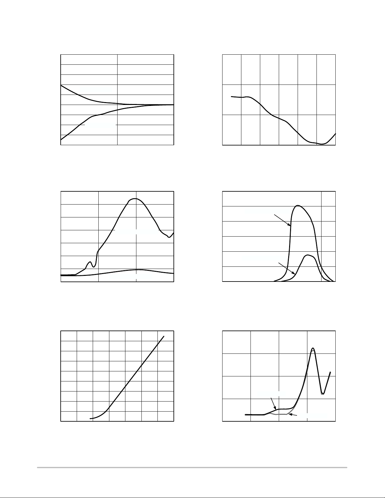
TYPICAL PERFORMANCE CHARACTERISTICS
20
16
12
8
4
0
−4
−8
TEMPERATURE ERROR (°C)
−12
−16
0 10 100
D+ To GND
D+ To V
DD
LEAKAGE RESISTANCE (MW)
Figure 3. Temperature Error vs. Leakage
Resistance
13
11
9
TEMPERATURE ERROR (°C)
−1
7
5
3
1
100K
1M 10M 100M
FREQUENCY (Hz)
VIN = 40 mV p−p
VIN = 10 mV p−p
Figure 5. Temperature Error vs. Differential Mode
Noise Frequency
1.0
0.5
0
TEMPERATURE ERROR (°C)
−0.5
0
20 40 60 80 100 120
TEMPERATURE (°C)
Figure 4. Temperature Error vs. Actual
Temperature Using 2N3906
12
TEMPERATURE ERROR (°C)
10
8
6
4
2
0
10
VIN = 250 mV p−p
VIN = 100 mV p−p
1M
FREQUENCY (Hz)
Figure 6. Temperature Error vs. Power Supply
Noise Frequency
18
16
14
12
10
8
6
4
TEMPERATURE ERROR (°C)
2
0
6111621263136
1
CAPACITANCE (nF)
Figure 7. Temperature Error vs. Capacitance
Between D+ and D−
2.0
1.5
1.0
0.5
SUPPLY CURRENT (mA)
0.0
http://onsemi.com
5
VDD = 5 V
VDD = 3 V
0.01
0.1 1 10 100
CONVERSION RATE (Hz)
Figure 8. Operating Supply Current vs.
Conversion Rate
ADM1032
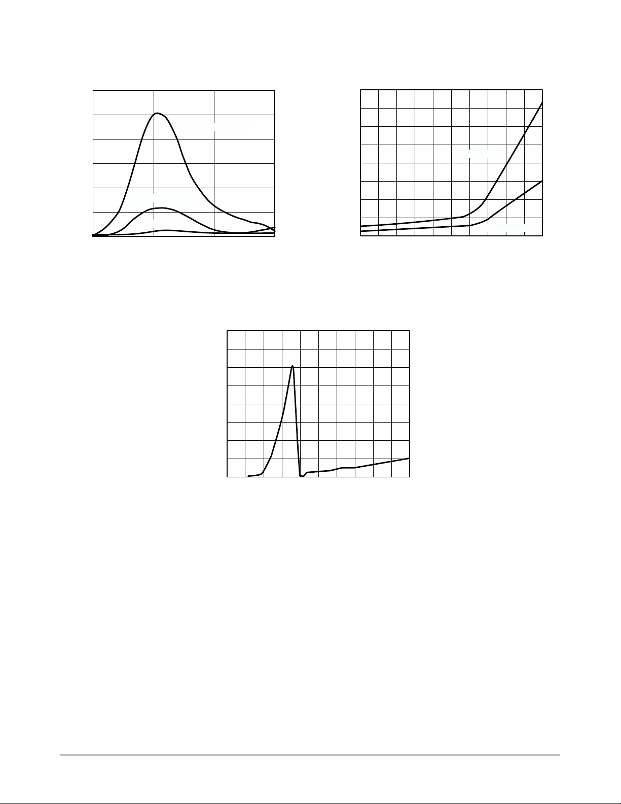
TYPICAL PERFORMANCE CHARACTERISTICS (Cont’d)
12
10
VIN = 100 mV p−p
8
6
TEMPERATURE ERROR (°C)
4
2
0
100K
VIN = 50 mV p−p
VIN = 25 mV p−p
1M 10M 100M
FREQUENCY (Hz)
Figure 9. Temperature Error vs. Common-mode
Noise Frequency
40
35
30
25
80
70
60
SUPPLY CURRENT (mA)
50
40
30
20
10
0
5 10 25 50 75 100 250 500 750 1000
1
SCLK FREQUENCY (kHz)
VDD = 5 V
VDD = 3.3 V
Figure 10. Standby Supply Current vs. Clock
Frequency
20
15
10
5
STANDBY SUPPLY CURRENT (mA)
0
0
0.5 1.0 1.5 2.0 2.5 3.0 3.5 4.0 4.5 5.0
SUPPLY VOLTAGE (V)
Figure 11. Standby Supply Current vs. Supply Voltage
http://onsemi.com
6

ADM1032
Functional Description
The ADM1032 is a local and remote temperature sensor
and overtemperature alarm. When the ADM1032 is
operating normally, the on-board A/D converter operates in
a free running mode. The analog input multiplexer
alternately selects either the on-chip temperature sensor to
measure its local temperature or the remote temperature
sensor. These signals are digitized by the ADC, and the
results are stored in the local and remote temperature value
registers.
The measurement results are compared with local and
remote, high, low, and THERM
temperature limits stored in
nine on-chip registers. Out-of-limit comparisons generate
flags that are stored in the status register, and one or more
out-of-limit results cause the ALERT
Exceeding THERM
temperature limits causes the THERM
output to pull low.
output to assert low.
The limit registers can be programmed, and the device
controlled and configured, via the serial SMBus. The
contents of any register can also be read back via the SMBus.
Control and configuration functions consist of:
• Switching the Device between Normal Operation and
Standby Mode
• Masking or Enabling the ALERT Output
• Selecting the Conversion Rate
Measurement Method
A simple method of measuring temperature is to exploit
the negative temperature coefficient of a diode, or the
base-emitter voltage of a transistor, operated at constant
current. Unfortunately, this technique requires calibration to
null out the effect of the absolute value of V
from device to device.
The technique used in the ADM1032 is to measure the
change in V
when the device is operated at two different
BE
currents.
, which varies
BE
This is given by:
DVBE+ǒn
Ǔ
f
q
In(N
)
(eq. 1)
KT
where:
–23
K is Boltzmann’s constant (1.38 × 10
q is the charge on the electron (1.6 × 10
)
–19
Coulombs)
T is the absolute temperature in Kelvins
N is the ratio of the two currents
n
is the ideality factor of the thermal diode.
f
The ADM1032 is trimmed for an ideality factor of 1.008.
Figure 12 shows the input signal conditioning used to
measure the output of an external temperature sensor.
Figure 12 shows the external sensor as a substrate transistor,
provided for temperature monitoring on some
microprocessors, but it could equally well be a discrete
transistor. If a discrete transistor is used, the collector is not
grounded and should be linked to the base. To prevent
ground noise interfering with the measurement, the more
negative terminal of the sensor is not referenced to ground
but is biased above ground by an internal diode at the D−
input. If the sensor is operating in a noisy environment, C1
can optionally be added as a noise filter. Its value should be
no more than 1000 pF. See the Layout Considerations
section for more information on C1.
To measure DV
, the sensor is switched between the
BE
operating currents of I and N × I. The resulting waveform is
passed through a 65 kHz low-pass filter to remove noise, and
then to a chopper-stabilized amplifier that performs the
functions of amplification and rectification of the waveform
to produce a dc voltage proportional to DV
. This voltage
BE
is measured by the ADC to give a temperature output in twos
complement format. To further reduce the effects of noise,
digital filtering is performed by averaging the results of 16
measurement cycles.
Signal conditioning and measurement of the internal
temperature sensor is performed in a similar manner.
V
= 65 kHz
f
C
DD
IN × I
D+
REMOTE
SENSING
TRANSISTOR
* CAPACITOR C1 IS OPTIONAL AND IT SHOULD ONLY BE USED IN VERY NOISY ENVIRONMENTS. C1 = 1000 pF Max.
C1*
D−
DIODE
Figure 12. Input Signal Conditioning
I
BIAS
BIAS
LOW-PASS FILTER
http://onsemi.com
7
V
OUT+
To ADC
V
OUT−

ADM1032
Temperature Data Format
One LSB of the ADC corresponds to 0.125°C, so the ADC
can measure from 0°C to 127.875°C. The temperature data
format is shown in Table 5 and Table 6.
The results of the local and remote temperature
measurements are stored in the local and remote temperature
value registers and are compared with limits programmed
into the local and remote high and low limit registers.
Table 5. TEMPERATURE DATA FORMAT
(LOCAL TEMPERATURE AND REMOTE
TEMPERATURE HIGH BYTE)
Temperature Digital Output
0°C 0 000 0000
1°C 0 000 0001
10°C 0 000 1010
25°C 0 001 1001
50°C 0 011 0010
75°C 0 100 1011
100°C 0 110 0100
125°C 0 111 1101
127°C 0 111 1111
Table 6. EXTENDED TEMPERATURE RESOLUTION
(REMOTE TEMPERATURE LOW BYTE)
Remote Temperature
Extended Resolution
0.000°C 0 000 0000
0.125°C 0 010 0000
0.250°C 0 100 0000
0.375°C 0 110 0000
0.500°C 1 000 0000
0.625°C 1 010 0000
0.750°C 1 100 0000
0.875°C 1 110 0000
ADM1032 Registers
Low Byte
The ADM1032 contains registers that are used to store the
results of remote and local temperature measurements and
high and low temperature limits and to configure and control
the device. A description of these registers follows, and
further details are given in Table 7 to Table 11.
Address Pointer Register
The address pointer register itself does not have, or
require, an address because it is the register the first data byte
of every write operation is written to automatically. This
data byte is an address pointer that sets up one of the other
registers for the second byte of the write operation or for a
subsequent read operation.
The power-on default value of the address pointer register
is 00h. Therefore, if a read operation is performed
immediately after power-on without first writing to the
address pointer, the value of the local temperature is returned
because its register address is 00h.
Value Registers
The ADM1032 has three registers to store the results of
local and remote temperature measurements. These
registers are written to by the ADC only and can be read over
the SMBus.
Offset Register
Series resistance on the D+ and D− lines in processor
packages and clock noise can introduce offset errors into the
remote temperature measurement. To achieve the specified
accuracy on this channel, these offsets must be removed.
The offset value is stored as an 11-bit, twos complement
value in Register 11h (high byte) and Register 12h (low
byte, left justified). The value of the offset is negative if the
MSB of Register 11h is 1 and positive if the MSB of
Register 12h is 0. The value is added to the measured value
of the remote temperature.
The offset register powers up with a default value of 0°C
and has no effect if nothing is written to them.
Table 7. SAMPLE OFFSET REGISTER CODES
Offset Value 11h 12h
−4°C 1 111 1100 0 000 0000
−1°C 1 111 1111 0 000 0000
−0.125°C 1 111 1111 1 110 0000
0°C 0 000 0000 0 000 0000
+0.125°C 0 000 0000 0 010 0000
+1°C 0 000 0001 0 000 0000
+4°C 0 000 0100 0 000 0000
Status Register
Bit 7 of the status register indicates that the ADC is busy
converting when it is high. Bit 6 to Bit 3, Bit 1, and Bit 0 are
flags that indicate the results of the limit comparisons. Bit 2
is set when the remote sensor is open circuit.
If the local and/or remote temperature measurement is
above the corresponding high temperature limit, or below or
equal to the corresponding low temperature limit, one or
more of these flags is set. These five flags (Bit 6 to Bit 2) are
NOR’ed together, so that if any of them are high, the ALERT
interrupt latch is set and the ALERT output goes low.
Reading the status register clears the five flag bits, provided
that the error conditions that caused the flags to be set have
gone away. While a limit comparator is tripped due to a value
register containing an out-of-limit measurement, or the
sensor is open circuit, the corresponding flag bit cannot be
reset. A flag bit can only be reset if the corresponding value
register contains an in-limit measurement or the sensor is
good.
The ALERT
status register but is reset when the ALERT
interrupt latch is not reset by reading the
output is
serviced by the master reading the device address, provided
the error condition has gone away and the status register flag
bits are reset.
When Flag 1 and Flag 0 are set, the THERM
output goes
low to indicate that the temperature measurements are
http://onsemi.com
8

ADM1032
outside the programmed limits. THERM output does not
need to be reset, unlike the ALERT
output. Once the
measurements are within the limits, the corresponding status
register bits are reset and the THERM
Table 8. STATUS REGISTER BIT ASSIGNMENTS
Bit Name Function
7 BUSY 1 When ADC Converting
6 LHIGH
(Note 1)
5 LLOW
(Note 1)
4 RHIGH
(Note 1)
3 RLOW
(Note 1)
2 OPEN
(Note 1)
1 RTHRM 1 When Remote THERM Limit Tripped
0 LTHRM1 1 When Local THERM Limit Tripped
1. These flags stay high until the status register is read, or they are
reset by POR.
Configuration Register
1 When Local High Temp Limit Tripped
1 When Local Low Temp Limit Tripped
1 When Remote High Temp Limit
Tripped
1 When Remote Low Temp Limit
Tripped
1 When Remote Sensor Open-Circuit
output goes high.
Two bits of the configuration register are used. If Bit 6 is
0, which is the power-on default, the device is in operating
mode with the ADC converting. If Bit 6 is set to 1, the device
is in standby mode and the ADC does not convert. The
SMBus does, however, remain active in standby mode so
values can be read from or written to the SMBus. The
ALERT
and THERM O/Ps are also active in standby mode.
Bit 7 of the configuration register is used to mask the alert
output. If Bit 7 is 0, which is the power-on default, the output
is enabled. If Bit 7 is set to 1, the output is disabled.
Table 9. CONFIGURATION REGISTER BIT
ASSIGNMENTS
Power-On
Bit Name Function
7 MASK1 0 = ALERT Enabled
6 RUN/STOP 0 = Run
5 to 0 Reserved 0
Conversion Rate Register
1 = ALERT
1 = Standby
Masked
Default
0
0
The lowest four bits of this register are used to program the
conversion rate by dividing the internal oscillator clock by
1, 2, 4, 8, 16, 32, 64, 128, 256, 512, or 1024 to give
conversion times from 15.5 ms (Code 0Ah) to 16 seconds
(Code 00h). This register can be written to and read back
over the SMBus. The higher four bits of this register are
unused and must be set to 0. Use of slower conversion times
greatly reduces the device power consumption, as shown in
Table 10.
Table 10. CONVERSION RATE REGISTER CODES
Data Conversion/Sec Average Supply Current
mA Typ at V
00h 0.0625 0.17
01h 0.125 0.20
02h 0.25 0.21
03h 0.5 0.24
04h 1 0.29
05h 2 0.40
06h 4 0.61
07h 8 1.1
08h 16 1.9
09h 32 0.73
0Ah 64 1.23
0B to FFh Reserved
Limit Registers
= 5.5 V
DD
The ADM1032 has nine limit registers to store local and
remote, high, low, and THERM
temperature limits. These
registers can be written to and read back over the SMBus.
The high limit registers perform a > comparison, while the
low limit registers perform a < or = to comparison. For
example, if the high limit register is programmed with 80°C,
measuring 81°C results in an alarm condition. If the low
limit register is programmed with 0°C, measuring 0°C or
lower results in an alarm condition. Exceeding either the
local or remote THERM
limit asserts THERM low. A
default hysteresis value of 10°C is provided, which applies
to both channels. This hysteresis can be reprogrammed to
any value after powerup (Reg 0x21h).
One-Shot Register
The one-shot register is used to initiate a single conversion
and comparison cycle when the ADM1032 is in standby
mode, after which the device returns to standby. This is not
a data register as such, and it is the write operation that
causes the one-shot conversion. The data written to this
address is irrelevant and is not stored. The conversion time
on a single shot is 96 ms when the conversion rate is 16
conversions per second or less. At 32 conversions per
second, the conversion time is 15.3 ms. This is because
averaging is disabled at the faster conversion rates (32 and
64 conversions per second).
Consecutive ALERT Register
This value written to this register determines how many
out-of limit measurements must occur before an ALERT
is
generated. The default value is that one out-of-limit
measurement generates an ALERT
. The maximum value
that can be chosen is four. The purpose of this register is to
allow the user to perform some filtering of the output. This
is particularly useful at the faster two conversion rates where
no averaging takes place.
http://onsemi.com
9

ADM1032
Table 11. CONSECUTIVE ALERT REGISTER CODES
Number of Out-of-Limit
Register Value
yxxx 000x 1
yxxx 001x 2
yxxx 011x 3
yxxx 111x 4
NOTE: x = don’t care bits, and y = SMBus timeout bit.
Default = 0. See SMBus section for more information.
Measurements Required
Serial Bus Interface
Control of the ADM1032 is carried out via the serial bus.
The ADM1032 is connected to this bus as a slave device,
under the control of a master device.
There is a programmable SMBus timeout. When this is
enabled, the SMBus times out after typically 25 ms of no
activity. However, this feature is not enabled by default. To
enable it, set Bit 7 of the consecutive alert register
(Address = 22h).
Table 12. LIST OF ADM1032 REGISTERS
Read Address (Hex) Write Address (Hex) Name Power-On Default
Not Applicable Not Applicable Address Pointer Undefined
00 Not Applicable Local Temperature Value 0000 0000 (00h)
01 Not Applicable External Temperature Value High Byte 0000 0000 (00h)
02 Not Applicable Status Undefined
03 09 Configuration 0000 0000 (00h)
04 0A Conversion Rate 0000 1000 (08h)
05 0B Local Temperature High Limit 0101 0101 (55h) (85°C)
06 0C Local Temperature Low Limit 0000 0000 (00h) (0°C)
07 0D External Temperature High Limit High Byte 0101 0101 (55h) (85°C)
08 0E External Temperature Low Limit High Byte 0000 0000 (00h) (0°C)
Not Applicable 0F One-Shot
10 Not Applicable External Temperature Value Low Byte 0000 0000
11 11 External Temperature Offset High Byte 0000 0000
12 12 External Temperature Offset Low Byte 0000 0000
13 13 External Temperature High Limit Low Byte 0000 0000
14 14 External Temperature Low Limit Low Byte 0000 0000
19 19 External THERM Limit 0101 0101 (55h) (85°C) (ADM1032)
20 20 Local THERM Limit 0101 0101 (55h) (85°C)
21 21 THERM Hysteresis 0000 1010 (0Ah) (10°C)
22 22 Consecutive ALERT 0000 0001 (01h)
FE Not Applicable Manufacturer ID 0100 0001 (41h)
FF Not Applicable Die Revision Code Undefined
NOTE: Writing to Address 0F causes the ADM1032 to perform a single measurement. It is not a data register as such and it does not
matter what data is written to it.
0110 1100 (6Ch) (108°C)
(ADM1032−1)
Addressing the Device
In general, every SMBus device has a 7-bit device address
(except for some devices that have extended, 10-bit
addresses). When the master device sends a device address
over the bus, the slave device with that address responds.
The ADM1032 and the ADM1032−1 are available with one
SMBus address, which is Hex 4C (1001 100). The
ADM1032−2 is also available with one SMBus address;
however, that address is Hex 4D (1001 101).
http://onsemi.com
The serial bus protocol operates as follows:
1. The master initiates data transfer by establishing a
START condition, defined as a high-to-low
transition on the serial data line SDATA, while the
serial clock line SCLK remains high. This
indicates that an address/data stream follows. All
slave peripherals connected to the serial bus
respond to the START condition and shift in the
next eight bits, consisting of a 7-bit address (MSB
first) plus an R/W
10
bit, which determines the

ADM1032
direction of the data transfer, that is, whether data
is written to or read from the slave device.
The peripheral whose address corresponds to the
transmitted address responds by pulling the data
line low during the low period before the ninth
clock pulse, known as the acknowledge bit. All
other devices on the bus now remain idle while the
selected device waits for data to be read from or
written to it. If the R/W
to the slave device. If the R/W
bit is a 0, the master writes
bit is a 1, the
master reads from the slave device.
2. Data is sent over the serial bus in sequences of
nine clock pulses, eight bits of data followed by an
acknowledge bit from the slave device. Transitions
on the data line must occur during the low period
of the clock signal and remain stable during the
high period, since a low-to-high transition when
the clock is high can be interpreted as a STOP
signal. The number of data bytes that can be
transmitted over the serial bus in a single read or
write operation is limited only by what the master
and slave devices can handle.
3. When all data bytes are read or written, stop
conditions are established. In write mode, the
master pulls the data line high during the 10th
clock pulse to assert a STOP condition. In read
mode, the master device overrides the
acknowledge bit by pulling the data line high
during the low period before the ninth clock pulse.
This is known as no acknowledge. The master then
takes the data line low during the low period
before the 10th clock pulse, and high during the
10th clock pulse to assert a STOP condition.
Any number of bytes of data can be transferred over the
serial bus in one operation, but it is not possible to mix read
and write in one operation because the type of operation is
determined at the beginning and cannot subsequently be
changed without starting a new operation.
In the case of the ADM1032, write operations contain
either one or two bytes, while read operations contain one
byte and perform the following functions.
To write data to one of the device data registers or read
data from it, the address pointer register must first be set so
that the correct data register is addressed. The first byte of
a write operation always contains a valid address that is
stored in the address pointer register. If data is written to the
device, the write operation contains a second data byte that
is written to the register selected by the address pointer
register.
This is illustrated in Figure 13. The device address is sent
over the bus followed by R/W
set to 0. This is followed by
two data bytes. The first data byte is the address of the
internal data register to be written to, which is stored in the
address pointer register. The second data byte is the data to
be written to the internal data register.
When reading data from a register, there are two
possibilities:
1. If the address pointer register value is unknown or
not the desired value, it is first necessary to set it
to the correct value before data can be read from
the desired data register. This is done by
performing a write to the ADM1032 as before, but
only the data byte containing the register read
address is sent because data is not to be written to
the register. This is shown in Figure 14.
A read operation is then performed consisting of
the serial bus address, R/W
bit set to 1, followed
by the data byte read from the data register. This is
shown in Figure 15.
2. If the address pointer register is known to be at the
desired address already, data can be read from the
corresponding data register without first writing to
the address pointer register and Figure 14 can be
omitted.
NOTES:
1. Although it is possible to read a data byte from a data
register without first writing to the address pointer register,
if the address pointer register is already at the correct value,
it is not possible to write data to a register without writing to
the address pointer register. The first data byte of a write is
always written to the address pointer register.
2. Don’t forget that some of the ADM1032 registers have
different addresses for read and write operations. The write
address of a register must be written to the address pointer
if data is to be written to that register, but it is not possible
to read data from that address. The read address of a
register must be written to the address pointer before data
can be read from that register.
http://onsemi.com
11

ADM1032
SCLK
SDATA
SCLK
SDATA
START BY
MASTER
START BY
MASTER
191
A6
A5 A4
A3
FRAME 1
SERIAL BUS ADDRESS BYTE
SCLK (CONTINUED)
SDATA (CONTINUED)
A2
A0
A1
R/W
ACK. BY
ADM1032
1
D7
D6
D7
D5
D6
D4
D5
ADDRESS POINTER REGISTER BYTE
D4
D3
FRAME 3
DATA BYTE
D3
FRAME 2
D2
D2
D1
D1
D0
ADM1032
Figure 13. Writing a Register Address to the Address Pointer Register,
then Writing Data to the Selected Register
19
A2A3A4A5A6
FRAME 1
SERIAL BUS ADDRESS BYTE
A0
A1
R/W
ACK. BY
ADM1032
1
D6
D7
D4
D5
ADDRESS POINTER REGISTER BYTE
D3
FRAME 2
D2
D1
D0
D0
9
ACK. BY
ACK. BY
ADM1032
9
ACK. BY
ADM1032
STOP BY
MASTER
9
STOP BY
MASTER
Figure 14. Writing to the Address Pointer Register Only
SCLK
SDATA
START BY
MASTER
1
A2A3A4A5A6
A1 A0
FRAME 1
SERIAL BUS ADDRESS BYTE
R/W
Figure 15. Reading Data from a Previously Selected Register
ALERT Output
The ALERT output goes low whenever an out-of-limit
measurement is detected, or if the remote temperature sensor
is open-circuit. It is an open drain and requires a pullup to
V
. Several ALERT outputs can be wire-OR’ed together
DD
so that the common line goes low if one or more of the
ALERT
processor, or it can be used as an SMBALERT
outputs goes low.
The ALERT
output can be used as an interrupt signal to a
. Slave devices
on the SMBus can not normally signal to the master that they
want to talk, but the SMBALERT
function allows them to do
so.
One or more ALERT
common SMBALERT
the SMBALERT
line is pulled low by one of the devices, the
outputs can be connected to a
line connected to the master. When
following procedure occurs (see Figure 16).
9
ACK. BY
ADM1032
1
D7
D6
MASTER
RECEIVES
SMBALERT
D3
FRAME 2
D2
D4
D5
DATA BYTE FROM ADM1032
ALERT RESPONSE
ADDRESS
MASTER SENDS
ARA AND READ
COMMAND
D1
RDSTART ACK
9
D0
ACK. BY
ADM1032
DEVICE
ADDRESSNOACK
DEVICE SENDS
ITS ADDRESS
Figure 16. Use of SMBALERT
1. SMBALERT is pulled low.
2. Master initiates a read operation and sends the
alert response address (ARA = 0001 100). This is
a general call address that must not be used as a
specific device address.
3. The device whose ALERT
output is low responds
to the alert response address and the master reads
its device address. Since the device address is
STOP BY
MASTER
STOP
http://onsemi.com
12

ADM1032
seven bits, an LSB of 1 is added. The address of
the device is now known, and it can be
interrogated in the usual way.
4. If more than one device’s ALERT
output is low,
the one with the lowest device address has priority
in accordance with normal SMBus arbitration.
5. Once the ADM1032 has responded to the alert
response address, it resets its ALERT
output,
provided that the error condition that caused the
ALERT
no longer exists. If the SMBALERT line
remains low, the master sends ARA again, and so
on until all devices whose ALERT
outputs were
low have responded.
Low Power Standby Mode
The ADM1032 can be put into a low power standby mode
by setting Bit 6 of the configuration register. When Bit 6 is
low, the ADM1032 operates normally. When Bit 6 is high,
the ADC is inhibited and any conversion in progress is
terminated without writing the result to the corresponding
value register.
The SMBus is still enabled. Power consumption in the
standby mode is reduced to less than 10 mA if there is no
SMBus activity, or 100 mA if there are clock and data signals
on the bus.
When the device is in standby mode, it is still possible to
initiate a one-shot conversion of both channels by writing
XXh to the one-shot register (Address 0Fh), after which the
device returns to standby. It is also possible to write new
values to the limit register while it is in standby. If the values
stored in the temperature value registers are now outside the
new limits, an ALERT
is generated even though the
ADM1032 is still in standby.
The ADM1032 Interrupt System
The ADM1032 has two interrupt outputs, ALERT and
THERM
. These have different functions. ALERT responds
to violations of software-programmed temperature limits
and is maskable. THERM
is intended as a fail-safe interrupt
output that cannot be masked.
If the temperature goes equal to or below the lower
temperature limit, the ALERT
pin is asserted low to indicate
an out-of-limit condition. If the temperature is within the
programmed low and high temperature limits, no interrupt
is generated.
If the temperature exceeds the high temperature limit, the
ALERT
condition. A local and remote THERM
pin is asserted low to indicate an overtemperature
limit can be
programmed into the device to set the temperature limit
above which the overtemperature THERM
pin is asserted
low. This temperature limit should be equal to or greater than
the high temperature limit programmed.
The behavior of the high limit and THERM
limit is as
follows:
1. If either temperature measured exceeds the high
temperature limit, the ALERT
output is asserted
low.
2. If the local or remote temperature continues to
increase and either one exceeds the THERM
the THERM
output asserts low. This can be used
limit,
to throttle the CPU clock or switch on a fan.
A THERM
hysteresis value is provided to prevent a
cooling fan cycling on and off. The power-on default value
is 10°C, but this can be reprogrammed to any value after
powerup. This hysteresis value applies to both the local and
remote channels.
Using these two limits in this way, allows the user to gain
maximum performance from the system by only slowing it
down should it be at a critical temperature.
The THERM
V
. The THERM signal must always be pulled up to the
DD
signal is open drain and requires a pullup to
same power supply as the ADM1032, unlike the SMBus
signals (SDATA, SCLK, and ALERT
) that can be pulled to
a different power rail, usually that of the SMBus controller.
100°C
90°C
80°C
70°C
60°C
50°C
40°C
Table 13. THERM HYSTERESIS SAMPLE VALUES
Sensor Fault Detection
TEMPERATURE
Figure 17. Operation of the THERM Output
THERM Hysteresis Binary Representation
0°C 0 000 0000
1°C 0 000 0001
10°C 0 000 1010
LOCAL THERM LIMIT
LOCAL THERM
− HYSTERESIS
THERM
LIMIT
At the D+ input, the ADM1032 has a fault detector that
detects if the external sensor diode is open circuit. This is a
simple voltage comparator that trips if the voltage at D+
exceeds V
− 1.0 V (typical). The output of this
DD
comparator is checked when a conversion is initiated and
sets Bit 2 of the status register if a fault is detected.
If the remote sensor voltage falls below the normal
measuring range, for example, due to the diode being
short-circuited, the ADC outputs −128 (1000 0000). Since
the normal operating temperature range of the device only
extends down to 0°C, this output code should never be seen
in normal operation, so it can be interpreted as a fault
condition. Since it is outside the power-on default low
temperature limit (0°C) and any low limit that would
normally be programmed, a short-circuit sensor causes an
SMBus alert.
http://onsemi.com
13

ADM1032
In this respect, the ADM1032 differs from and improves
upon competitive devices that output zero if the external
sensor goes short-circuit. These devices can misinterpret a
genuine 0°C measurement as a fault condition.
When the D+ and D− lines are shorted together, an
ALERT
is always generated. This is because the remote
value register reports a temperature value of −128°C. Since
the ADM1032 performs a less-than or equal-to comparison
with the low limit, an ALERT
is generated even when the
low limit is set to its minimum of −128°C.
Applications Information − Factors Affecting
Accuracy
Remote Sensing Diode
The ADM1032 is designed to work with substrate
transistors built into processors’ CPUs or with discrete
transistors. Substrate transistors are generally PNP types
with the collector connected to the substrate. Discrete types
can be either a PNP or an NPN transistor connected as a
diode (base shorted to collector). If an NPN transistor is
used, the collector and base are connected to D+ and the
emitter to D−. If a PNP transistor is used, the collector and
base are connected to D− and the emitter to D+. Substrate
transistors are found in a number of CPUs. To reduce the
error due to variations in these substrate and discrete
transistors, a number of factors should be taken into
consideration:
1. The ideality factor, n
, of the transistor. The
f
ideality factor is a measure of the deviation of the
thermal diode from the ideal behavior. The
ADM1032 is trimmed for an n
value of 1.008.
f
The following equation can be used to calculate
the error introduced at a temperature T°C when
using a transistor whose n
Consult the processor data sheet for n
DT +
ǒ
n
natural
* 1.008
1.008
Ǔ
ǒ273.15 Kelvin ) T
does not equal 1.008.
f
values.
f
Ǔ
(eq. 2)
This value can be written to the offset register and
is automatically added to or subtracted from the
temperature measurement.
2. Some CPU manufacturers specify the high and
low current levels of the substrate transistors. The
high current level of the ADM1032, I
230 mA and the low level current, I
HIGH
LOW
, is
, is 13 mA.
If the ADM1032 current levels do not match the
levels of the CPU manufacturers, then it can
become necessary to remove an offset. The CPU’s
data sheet advises whether this offset needs to be
removed and how to calculate it. This offset can be
programmed to the offset register. It is important
to note that if accounting for two or more offsets is
needed, then the algebraic sum of these offsets
must be programmed to the offset register.
If a discrete transistor is being used with the ADM1032,
the best accuracy is obtained by choosing devices according
to the following criteria:
• Base-emitter Voltage Greater than 0.25 V at 6 mA, at
the Highest Operating Temperature
• Base-emitter Voltage Less than 0.95 V at 100 mA, at
the Lowest Operating Temperature
• Base Resistance Less than 100 W
• Small Variation in h
Tight Control of V
Transistors such as 2N3904, 2N3906, or equivalents in
SOT−23 packages are suitable devices to use.
Thermal Inertia and Self-heating
Accuracy depends on the temperature of the
remote-sensing diode and/or the internal temperature sensor
being at the same temperature as that being measured, and
a number of factors can affect this. Ideally, the sensor should
be in good thermal contact with the part of the system being
measured, for example, the processor. If it is not, the thermal
inertia caused by the mass of the sensor causes a lag in the
response of the sensor to a temperature change. In the case
of the remote sensor, this should not be a problem, since it
is either a substrate transistor in the processor or a small
package device, such as the SOT−23, placed in close
proximity to it.
The on-chip sensor, however, is often remote from the
processor and is only monitoring the general ambient
temperature around the package. The thermal time constant
of the SOIC−8 package in still air is about 140 seconds, and
if the ambient air temperature quickly changed by 100°, it
would take about 12 minutes (five time constants) for the
junction temperature of the ADM1032 to settle within 1° of
this. In practice, the ADM1032 package is in electrical and
therefore thermal contact with a printed circuit board and
can also be in a forced airflow. How accurately the
temperature of the board and/or the forced airflow reflect the
temperature to be measured also affects the accuracy.
Self-heating due to the power dissipated in the ADM1032
or the remote sensor causes the chip temperature of the
device or remote sensor to rise above ambient. However, the
current forced through the remote sensor is so small that
self-heating is negligible. In the case of the ADM1032, the
worst-case condition occurs when the device is converting
at 16 conversions per second while sinking the maximum
current of 1 mA at the ALERT
case, the total power dissipation in the device is about
11 mW. The thermal resistance, q
is about 121°C/W.
In practice, the package has electrical and therefore
thermal connection to the printed circuit board, so the
temperature rise due to self-heating is negligible.
(say 50 to 150) that Indicates
FE
Characteristics
BE
and THERM output. In this
, of the SOIC−8 package
JA
http://onsemi.com
14

ADM1032
Layout Considerations
Digital boards can be electrically noisy environments, and
the ADM1032 is measuring very small voltages from the
remote sensor, so care must be taken to minimize noise
induced at the sensor inputs. The following precautions
should be taken.
1. Place the ADM1032 as close as possible to the
remote sensing diode. Provided that the worst
noise sources, that is, clock generators,
data/address buses, and CRTs, are avoided, this
distance can be four to eight inches.
2. Route the D+ and D− tracks close together, in
parallel, with grounded guard tracks on each side.
Provide a ground plane under the tracks if
possible.
3. Use wide tracks to minimize inductance and
reduce noise pickup. 10 mil track minimum width
and spacing is recommended.
GND
D+
D−
GND
Figure 18. Typical Arrangement of Signal Tracks
10 MIL
10 MIL
10 MIL
10 MIL
10 MIL
10 MIL
10 MIL
4. Try to minimize the number of copper/solder
joints, which can cause thermocouple effects.
Where copper/solder joints are used, make sure
that they are in both the D+ and D− path and at the
same temperature.
Thermocouple effects should not be a major
problem since 1°C corresponds to about 200 mV
and thermocouple voltages are about 3 mV/°C of
temperature difference. Unless there are two
thermocouples with a big temperature differential
between them, thermocouple voltages should be
much less than 200 mV.
5. Place a 0.1 mF bypass capacitor close to the V
DD
pin. In very noisy environments, place a 1000 pF
input filter capacitor across D+ and D− close to the
ADM1032.
6. If the distance to the remote sensor is more than
eight inches, the use of twisted pair cable is
recommended. This works up to about 6 feet to
12 feet.
7. For really long distances (up to 100 feet), use
shielded twisted pair, such as Belden #8451
microphone cable. Connect the twisted pair to D+
and D− and the shield to GND close to the
ADM1032. Leave the remote end of the shield
unconnected to avoid ground loops.
Because the measurement technique uses switched
current sources, excessive cable and/or filter capacitance
can affect the measurement. When using long cables, the
filter capacitor can be reduced or removed.
Cable resistance can also introduce errors. 1 W series
resistance introduces about 1°C error.
Power Sequencing Considerations
Power Supply Slew Rate
When powering up the ADM1032 you must ensure that
the slew rate of V
is less than 18 mV/ms. A slew rate larger
DD
than this may cause power-on-reset issues and yield
unpredictable results.
THERM Pin Pullup
As mentioned above, the THERM signal is open drain and
requires a pullup to V
. The THERM signal must always
DD
be pulled up to the same power supply as the ADM1032,
unlike the SMBus signals (SDA, SCL and ALERT
) that can
be pulled to a different power rail. The only time the
THERM
than V
with, or after the ADM1032 main V
internal circuitry of the ADM1032. If the THERM
supply rail were to rise before V
pin can be pulled to a different supply rail (other
) is if the other supply is powered up simultaneous
DD
. This is to protect the
DD
pullup
, the POR circuitry may
DD
not operate correctly.
Application Circuit
Figure 19 shows a typical application circuit for the
ADM1032, using a discrete sensor transistor connected via
a shielded, twisted pair cable. The pullups on SCLK,
SDATA, and ALERT
are required only if they are not
already provided elsewhere in the system.
The SCLK and SDATA pins of the ADM1032 can be
interfaced directly to the SMBus of an I/O controller, such
as the Intel 820 chipset.
http://onsemi.com
15

ADM1032
0.1 mF
V
DD
3 V to 3.6 V
TYP 10 kW
SMBUS
CONTROLLER
5 V or 12 V
FAN
CONTROL
CIRCUIT
or
CPU THERMAL
DIODE
ADM1032
D+
D−
SHIELD2N3906
GND
SCLK
SDATA
ALERT
THERM
V
DD
FAN
ENABLE
TYP 10 kW
Figure 19. Typical Application Circuit
Table 14. ORDERING INFORMATION
Package
Device Order Number*
ADM1032ARZ−REEL 8-lead SOIC NB R−8 #1 4C 2,500 Tape & Reel 85°C
ADM1032ARZ−1REEL 8-lead SOIC NB R−8 #2 4C 2,500 Tape & Reel 108°C
ADM1032ARMZ−REEL 8-lead MSOP RM−8 T1J 4C 3,000 Tape & Reel 85°C
ADM1032ARMZ−1RL 8-lead MSOP RM−8 T13 4C 3,000 Tape & Reel 108°C
ADM1032ARMZ−2R 8-lead MSOP RM−8 T1C 4D 3,000 Tape & Reel 85°C
*The “Z’’ suffix indicates Pb-Free package.
†For information on tape and reel specifications, including part orientation and tape sizes, please refer to our Tape and Reel Packaging
Specifications Brochure, BRD8011/D.
Description
Package
Option
Part
Marking
SMBus
Address
Shipping
†
External THERM
Default
http://onsemi.com
16

−Y−
−Z−
ADM1032
PACKAGE DIMENSIONS
SOIC−8 NB
CASE 751−07
ISSUE AK
NOTES:
−X−
A
58
B
1
S
0.25 (0.010)
4
M
M
Y
K
G
C
SEATING
PLANE
0.10 (0.004)
H
D
0.25 (0.010) Z
M
Y
SXS
N
X 45
_
M
J
1. DIMENSIONING AND TOLERANCING PER
ANSI Y14.5M, 1982.
2. CONTROLLING DIMENSION: MILLIMETER.
3. DIMENSION A AND B DO NOT INCLUDE
MOLD PROTRUSION.
4. MAXIMUM MOLD PROTRUSION 0.15 (0.006)
PER SIDE.
5. DIMENSION D DOES NOT INCLUDE DAMBAR
PROTRUSION. ALLOWABLE DAMBAR
PROTRUSION SHALL BE 0.127 (0.005) TOTAL
IN EXCESS OF THE D DIMENSION AT
MAXIMUM MATERIAL CONDITION.
6. 751−01 THRU 751−06 ARE OBSOLETE. NEW
STANDARD IS 751−07.
MILLIMETERS
DIMAMIN MAX MIN MAX
4.80 5.00 0.189 0.197
B 3.80 4.00 0.150 0.157
C 1.35 1.75 0.053 0.069
D 0.33 0.51 0.013 0.020
G 1.27 BSC 0.050 BSC
H 0.10 0.25 0.004 0.010
J 0.19 0.25 0.007 0.010
K 0.40 1.27 0.016 0.050
M 0 8 0 8
____
N 0.25 0.50 0.010 0.020
S 5.80 6.20 0.228 0.244
INCHES
SOLDERING FOOTPRINT*
1.52
0.060
7.0
0.275
0.6
0.024
*For additional information on our Pb-Free strategy and soldering
details, please download the ON Semiconductor Soldering and
Mounting Techniques Reference Manual, SOLDERRM/D.
4.0
0.155
1.270
0.050
SCALE 6:1
ǒ
inches
mm
Ǔ
http://onsemi.com
17

ADM1032
PACKAGE DIMENSIONS
MSOP8
CASE 846AB
ISSUE O
SEATING
PLANE
−T−
0.038 (0.0015)
PIN 1 ID
DD
H
E
e
E
8 PL
b
0.08 (0.003) A
M
T
S
B
S
NOTES:
1. DIMENSIONING AND TOLERANCING PER ANSI Y14.5M, 1982.
2. CONTROLLING DIMENSION: MILLIMETER.
3. DIMENSION A DOES NOT INCLUDE MOLD FLASH, PROTRUSIONS OR GATE
BURRS. MOLD FLASH, PROTRUSIONS OR GATE BURRS SHALL NOT EXCEED
0.15 (0.006) PER SIDE.
4. DIMENSION B DOES NOT INCLUDE INTERLEAD FLASH OR PROTRUSION.
INTERLEAD FLASH OR PROTRUSION SHALL NOT EXCEED 0.25 (0.010) PER SIDE.
5. 846A-01 OBSOLETE, NEW STANDARD 846A-02.
DIMAMIN NOM MAX MIN
A1 0.05 0.08 0.15 0.002
b 0.25 0.33 0.40 0.010
c 0.13 0.18 0.23 0.005
D 2.90 3.00 3.10 0.114
E 2.90 3.00 3.10 0.114
e 0.65 BSC
L 0.40 0.55 0.70 0.016
H
E
MILLIMETERS
−− −− 1.10 −−
4.75 4.90 5.05 0.187 0.193 0.199
INCHES
NOM MAX
−− 0.043
0.003 0.006
0.013 0.016
0.007 0.009
0.118 0.122
0.118 0.122
0.026 BSC
0.021 0.028
A
A1
c
L
SOLDERING FOOTPRINT*
8X
1.04
0.041
3.20
0.126
0.38
0.015
8X
4.24
0.167
5.28
0.208
0.65
6X
0.0256
SCALE 8:1
ǒ
inches
mm
Ǔ
*For additional information on our Pb-Free strategy and soldering
details, please download the ON Semiconductor Soldering and
Mounting Techniques Reference Manual, SOLDERRM/D.
ON Semiconductor and are registered trademarks of Semiconductor Components Industries, LLC (SCILLC). SCILLC reserves the right to make changes without further notice
to any products herein. SCILLC makes no warranty, representation or guarantee regarding the suitability of its products for any particular purpose, nor does SCILLC assume any liability
arising out of the application or use of any product or circuit, and specifically disclaims any and all liability, including without limitation special, consequential or incidental damages.
“Typical” parameters which may be provided in SCILLC data sheets and/or specifications can and do vary in different applications and actual performance may vary over time. All
operating parameters, including “Typicals” must be validated for each customer application by customer’s technical experts. SCILLC does not convey any license under its patent rights
nor the rights of others. SCILLC products are not designed, intended, or authorized for use as components in systems intended for surgical implant into the body, or other applications
intended to support or sustain life, or for any other application in which the failure of the SCILLC product could create a situation where personal injury or death may occur. Should
Buyer purchase or use SCILLC products for any such unintended or unauthorized application, Buyer shall indemnify and hold SCILLC and its officers, employees, subsidiaries, affiliates,
and distributors harmless against all claims, costs, damages, and expenses, and reasonable attorney fees arising out of, directly or indirectly, any claim of personal injury or death
associated with such unintended or unauthorized use, even if such claim alleges that SCILLC was negligent regarding the design or manufacture of the part. SCILLC is an Equal
Opportunity/Affirmative Action Employer. This literature is subject to all applicable copyright laws and is not for resale in any manner.
PUBLICATION ORDERING INFORMATION
LITERATURE FULFILLMENT:
Literature Distribution Center for ON Semiconductor
P.O. Box 5163, Denver, Colorado 80217 USA
Phone: 303−675−2175 or 800−344−3860 Toll Free USA/Canada
Fax: 303−675−2176 or 800−344−3867 Toll Free USA/Canada
Email: orderlit@onsemi.com
N. American Technical Support: 800−282−9855 Toll Free
USA/Canada
Europe, Middle East and Africa Technical Support:
Phone: 421 33 790 2910
Japan Customer Focus Center
Phone: 81−3−5817−1050
http://onsemi.com
ON Semiconductor Website: www.onsemi.com
Order Literature: http://www.onsemi.com/orderlit
For additional information, please contact your local
Sales Representative
ADM1032/D
18

 Loading...