ON 1SMA10AT3G, 1SMA11AT3G, 1SMA12AT3G, 1SMA13AT3G, 1SMA14AT3G Schematic [ru]
...
1SMA5.0AT3G Series,
SZ1SMA5.0AT3G Series
400 Watt Peak Power Zener
Transient Voltage
Suppressors
Unidirectional
The SMA series is designed to protect voltage sensitive
components from high voltage, high energy transients. They have
excellent clamping capability, high surge capability, low zener
impedance and fast response time. The SMA series is supplied in
ON Semiconductor’s exclusive, cost-effective, highly reliable
SURMETIC
communication systems, automotive, numerical controls, process
controls, medical equipment, business machines, power supplies and
many other industrial/consumer applications.
Features
Working Peak Reverse Voltage Range − 5.0 V to 78 V
Standard Zener Breakdown Voltage Range − 6.7 V to 91.25 V
Peak Power − 400 W @ 1 ms
ESD Rating of Class 3 (> 16 kV) per Human Body Model
Response Time is Typically < 1 ns
Flat Handling Surface for Accurate Placement
Package Design for Top Slide or Bottom Circuit Board Mounting
Low Profile Package
SZ Prefix for Automotive and Other Applications Requiring Unique
Site and Control Change Requirements; AEC−Q101 Qualified and
PPAP Capable
Pb−Free Packages are Available*
Mechanical Characteristics:
CASE:
FINISH: All external surfaces are corrosion resistant and leads are
readily solderable
MAXIMUM CASE TEMPERATURE FOR SOLDERING PURPOSES:
260C for 10 Seconds
POLARITY: Cathode indicated by molded polarity notch or polarity
band
MOUNTING POSITION: Any
package and is ideally suited for use in
Void-free, transfer-molded plastic
http://onsemi.com
PLASTIC SURFACE MOUNT
ZENER OVERVOLTAGE
TRANSIENT SUPPRESSORS
5.0 − 78 V, 400 W PEAK POWER
SMA
CASE 403D
STYLE 1
CATHODE ANODE
MARKING DIAGRAM
xx
AYWWG
xx = Device Code (Refer to page 3)
A = Assembly Location
Y = Year
WW = Work Week
G = Pb−Free Package
ORDERING INFORMATION
Device Package Shipping
1SMAxxAT3G SMA
SZ1SMAxxAT3G SMA
†For information on tape and reel specifications,
including part orientation and tape sizes, please
refer to our Tape and Reel Packaging Specifications
Brochure, BRD8011/D.
(Pb−Free)
(Pb−Free)
Tape & Reel
Tape & Reel
†
5,000 /
5,000 /
*For additional information on our Pb−Free strategy and soldering details, please
download the ON Semiconductor Soldering and Mounting Techniques
Reference Manual, SOLDERRM/D.
Semiconductor Components Industries, LLC, 2012
February, 2012 − Rev. 14
1 Publication Order Number:
DEVICE MARKING INFORMATION
See specific marking information in the device marking
column of the Electrical Characteristics table on page 3 of
this data sheet.
1SMA5.0AT3/D

1SMA5.0AT3G Series, SZ1SMA5.0AT3G Series
MAXIMUM RATINGS
Rating Symbol Value Unit
Peak Power Dissipation (Note 1) @ TL = 25C, Pulse Width = 1 ms P
DC Power Dissipation @ TL = 75C Measured Zero Lead Length (Note 2)
Derate Above 75C
Thermal Resistance from Junction to Lead
DC Power Dissipation (Note 3) @ TA = 25C
Derate Above 25C
Thermal Resistance from Junction to Ambient
Forward Surge Current (Note 4) @ TA = 25C I
Operating and Storage Temperature Range TJ, T
P
R
P
R
FSM
PK
D
q
JL
D
q
JA
stg
Stresses exceeding Maximum Ratings may damage the device. Maximum Ratings are stress ratings only. Functional operation above the
Recommended Operating Conditions is not implied. Extended exposure to stresses above the Recommended Operating Conditions may affect
device reliability.
1. 10 X 1000 ms, non−repetitive.
2. 1 square copper pad, FR−4 board.
3. FR−4 board, using ON Semiconductor minimum recommended footprint, as shown in 403B case outline dimensions spec.
4. 1/2 sine wave (or equivalent square wave), PW = 8.3 ms, duty cycle = 4 pulses per minute maximum.
400 W
1.5
20
50
0.5
4.0
250
W
mW/C
C/W
W
mW/C
C/W
40 A
−65 to +150 C
ELECTRICAL CHARACTERISTICS (T
otherwise noted, V
Symbol
I
PP
V
C
V
RWM
I
R
V
BR
I
T
I
F
V
F
= 3.5 V Max. @ IF = 30 A for all types) (Note 5)
F
Parameter
Maximum Reverse Peak Pulse Current
Clamping Voltage @ I
PP
Working Peak Reverse Voltage
Maximum Reverse Leakage Current @ V
Breakdown Voltage @ I
Test Current
Forward Current
Forward Voltage @ I
F
T
= 25C unless
A
RWM
5. 1/2 sine wave or equivalent, PW = 8.3 ms, non−repetitive duty
cycle.
VCV
V
RWM
BR
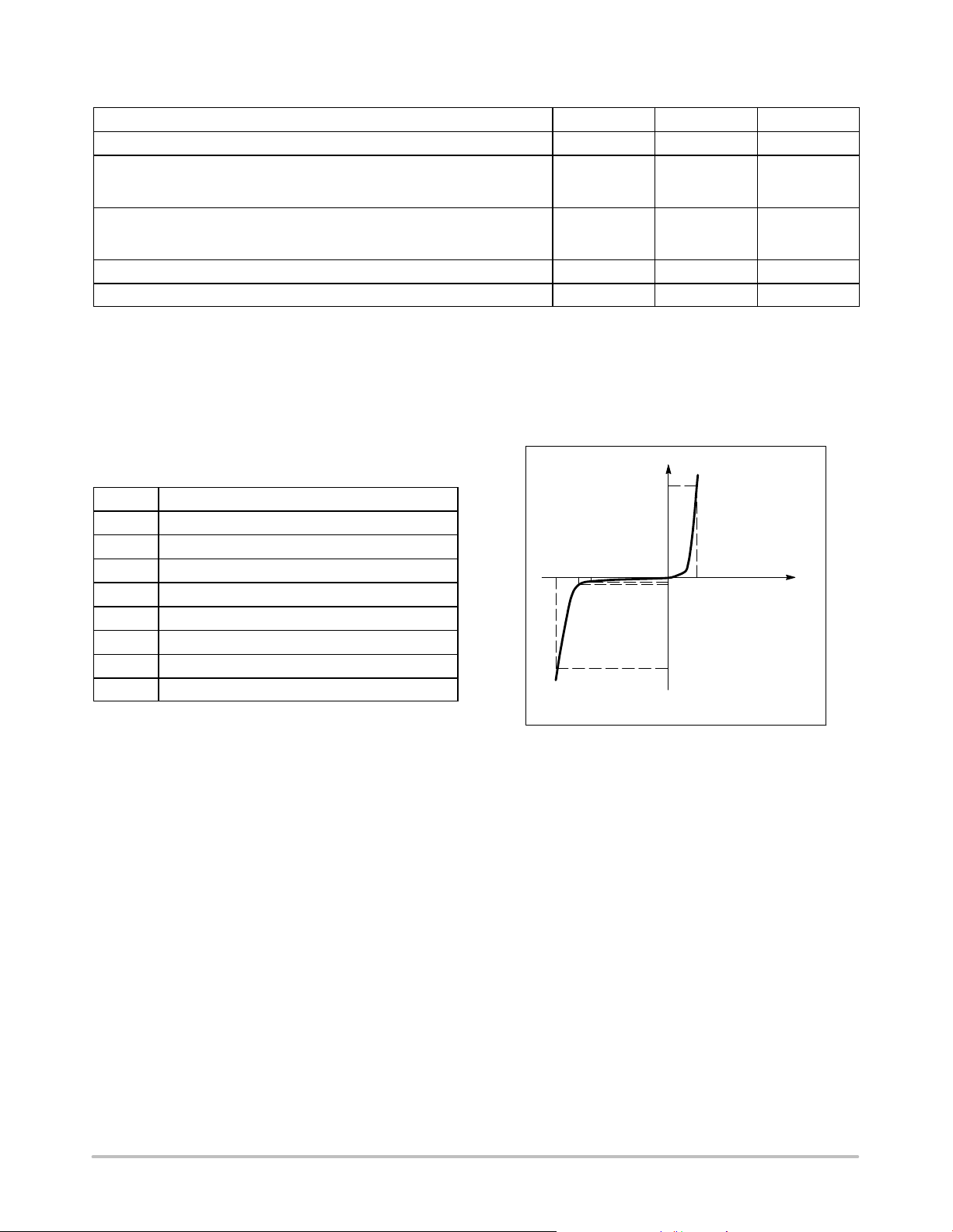
Uni−Directional TVS
I
I
F
I
V
R
F
I
T
I
PP
V
http://onsemi.com
2
 Loading...