


Cat. No. S921-E1-02
73T
s Manual
V720-series
Electromagnetic Inductive
RFID System
V720S-H MC73/V720S-HMC
PCB Read/Write Modules
User'

© OMRON,
2002
All rights reserved. No part of this publication may be reproduced, stored in a retrieval system, or transmitted, in any form, or
ts, the information contained in this manual is subject to change without
notice. Every precaution has been taken in the preparation of this manual. Nevertheless, OMRON assumes no responsibility
Notice:
OMRON products are manufactured for use according to proper procedures by a qualified operator and
only for the purposes described in this manual.
The following conventions are used to indicate and classify precautions in this manual. Always heed the
information provided with them. Failure to heed precautions can result in injury to people or damage to
property.
!
DANGER Indicates an imminently hazardous situation which, if not avoided, will result in death or
serious injury.
!
WARNING Indicates a pot entially hazardous situation which, if not avoided, could result in death or
serious injury.
!
Caution Indicates a potentially hazardous situation which, if not avoided, may result in minor or
moderate injury, or property damage.
Visual Aids
The following headings appear in the left column of the manual to help you locate different types of
information.
Note Indicates information of particular interest for efficient and convenient
operation of the product.
1, 2, 3... 1. Indicates lists of one sort or another, such as procedures, checklists, etc.
by any means, mechanical, electronic, photocopying, recording, or otherwise, without the prior written permission of
OMRON.
No patent liability is assumed with respect to the use of the information contained herein. Moreover, because OMRON is
constantly striving to improve its high-quality produc
for errors or omissions. Neither is any liability assumed for damages resulting from the use of the information contained in
this publication.
i

Failure to read and understand the information provided in this manual may result in
personal injury or death, damage to the product, or product failure. Please read
tion provided in
the section and related sections before attempting any of the procedures or
About this Manual:
This manual describes the installation and operation of the V720-series Electromagnetic Inductive
RFID System (V720S-HMC73/ V720S-HMC73T) and includes the sections described below.
Please read this manual carefully and be sure you understand the information provided before
attempting to install and operate the System.
Section 1 provides the features of the V720S-HMC73/ V720S -HMC73T.
Section 2 provides the specifications and performance characteristics of the V720S-HMC73/
V720S-HMC73T.
Section 3 provides the functions and operations of the V720S-HMC73/ V720S-HMC73T..
Section 4 provides the communications functions and provides details on communications–related
data and commands.
Section 5 provides the information of characteristics data.
!
WARNING
each section in its entirety and be sure you understand the informa
operations given.
?

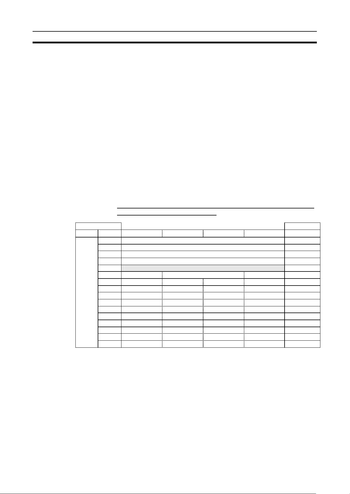
TABLE OF CONTENTS
PRECAUTION...................................................................................v
1. Intended Audience...................................................................................................................................vi
2. Regulations and Standards.....................................................................................................................vi
3. Application Precautions..........................................................................................................................vi
4. Precautions................................................................................................................................................vi
5. Correct Use ...............................................................................................................................................vi
SECTION 1
Product Outline ...............................................................................1-1
1-1 Features......................................................................................................................................................1-2
SECTION 2
Specifications and Performance...................................................2-1
2-1 Nomenclature and Descriptions............................................................................................................2-2
2-2 Specifications...........................................................................................................................................2-3
2-2-1 General Specifications.......................................................................................................................2-3
2-2-2 Interface Specifications.....................................................................................................................2-4
2-2-3 Interface Electrical Specifications ...................................................................................................2-5
2-2-4 Interface Circuit ..................................................................................................................................2-6
2-3 Dimensions ...............................................................................................................................................2-7
2-4 Antenna Center Position.........................................................................................................................2-8
SECTION 3
R/W Module Operations................................................................3-1
3-1 Outline of Operations..............................................................................................................................3-2
3-2 Tag Access Functions..............................................................................................................................3-3
3-2-1 Tag Memory Map...............................................................................................................................3-3
3-2-2 Single Access and FIFO Access Functions....................................................................................3-8
3-2-3 Lock Function.....................................................................................................................................3-9
3-2-4 Tag Identification Access Function.................................................................................................3-10
SECTION 4
Controlling the R/W Module ........................................................4-1
4-1 Communications Frames........................................................................................................................4-2
4-1-1 CR Control...........................................................................................................................................4-2
4-1-2 Number-of-characters Control.........................................................................................................4-2
4-2 Data Formats.............................................................................................................................................4-3
4-2-1 Command Code List ..........................................................................................................................4-3
4-2-2 Communications Options ..................................................................................................................4-5
4-2-3 End Code List......................................................................................................................................4-9
4-3 Commands and Responses during CR Control...................................................................................4-10
4-3-1 General Commands (Commands sent to RF Module).................................................................4-10
4-3-2 Commands Common to the I-CODE1 and the I-CODE2 Chips ................................................4-11
4-3-3 Commands Specific to the I-CODE2 Chip ....................................................................................4-15
4-3-4 Commands Specific to the I-CODE1 Chip ....................................................................................4-18
4-3-5 Old Commands Specific to the I-CODE1 Chip ............................................................................4-20
4-4 Commands and Responses during Number -of-characters Control.................................................4-24
4-4-1 General Commands (Commands sent to the RF Module)...........................................................4-24
4-4-2 Commands Common to the I-CODE1 and the I-CODE2 Chips ................................................4-25
4-4-3 Commands Specific to the I-CODE2 Chip ....................................................................................4-29
4-4-4 Commands Specific to the I-CODE1 Chip ....................................................................................4-32
4-4-5 Old Commands Specific to the I-CODE1 Chip ............................................................................4-34
iii

TABLE OF CONTENTS
SECTION 5
Characteristics Data (Reference)................................................5-1
5-1 Communications Distance (Reference)...............................................................................................5-2
5-2 Diagram of Communications Range (Reference)..............................................................................5-3
5-3 Communications Time (Reference)......................................................................................................5-6
5-3-1 Communications time........................................................................................................................5-6
5-3-2 TAT (Turn Around Time)..................................................................................................................5-8
5-4 Effects of Metal Backing Plate (Reference).......................................................................................5-9
5-5 Mutual Interference (Reference)...........................................................................................................5-10
5-6 Voltage Effects (Reference) ................................................................................................................... 5-11
Revision History
iv

PRECAUTION
This user manual provides information on the functions, characteristics, and application methods required to use
the V720S-HMC73 and V720S -HMC73T PCB Read/Write Modules.
In this manual, the PCB Read/Write Modules are referred to as simply R/W Modules.
Be sure to observe the following precaution when using the V720 Series.
Ÿ You must read this manual and understand the information contained before attempting to set up or operate a
V720-series Electromagnetic Inductive RFID System.
Ÿ Keep this manual close at hand for reference during operation.
1. Intended Audience .......................................................................................................................... vi
2. Regulations and Standards.............................................................................................................vi
3. Application Precautions.................................................................................................................vi
4. Precautions.....................................................................................................................................vi
5. Correct Use .....................................................................................................................................vi
v

1. Intended Audience
This manual is intended for the following personnel, who must also have knowledge of electrical systems (an
electrical engineer or the equivalent).
• Personnel in charge of installing systems.
• Personnel in charge of designing systems.
• Personnel in charge of managing systems and facilities.
2. Regulations and Standards
The V720S -HMC73 and V720S-HMC73T R/W Modules are combined with user devices and equipment
depending on the user application.
The user should check the conformity of devices with which the R/W Module has been combined with local
laws and regulations.
3. Application Precautions
Before using the product under the following conditions and environments, make sure that the ratings and
performance characteristics of the product are sufficient for the systems, machines, and equipment, be sure
to provide the systems, machines, and equipment with double safety mechanisms, and consult your
OMRON representative.
(1) When using the product under conditions and in environments that are not described in the manual
(2) When using the product for nuclear control systems, railroad systems, aviation systems, vehicles,
combustion systems, medical equipment, amusement machines, safety equipment
(3) When using the product for applications that may have a serious influence on people's lives and
property, especially those where safety is an issue.
!
WARNING Do not touch the PCB or any parts connected to the PCB while the power is being
supplied.Doing so may result in electric shock.
Do not attempt to take the product apart or insert or remove connectors while the power is
being supplied. Doing so may result in electric shock.
4. Precautions
Be sure to observe the following precautions to ensure safety in installing or operating the System.
1. Do not use the System in an environment subject to flammable, explosive, or corrosive gases.
2. Do not attempt to take any Units apart, to repair any Units, or to modify any Units in any way.
3. Be sure that all the mounting screws, terminal screws, and cable connector screws are tightened to the
torque specified in the relevant manuals.
4. Be sure that the power supply voltage is within the rated range (5 VDC ± 10%).
5. Observe all warnings, cautions, and safety precautions specified in the manual.
5. Correct Use
1. Do not install the R/W Module in the following locations:
Ÿ Locations subject to direct sunlight.
Ÿ Locations subject to condensation as the result of high humidity.
Ÿ Locations subject to shock or vibration.
2. Check the operating environment before use.
The R/W Module communicates with the tags using a frequency of 13.56 MHz. Noise that affects
communications with the tags may occur in transceivers, motors, monitor units, or power supplies (power
supply IC). If using the R/W Module close to these sources, check beforehand that the R/W Module is not
affected. Also, observe the following precautions to minimize the effects of noise.
Ÿ Connect any metal devices installed nearby to a ground of 100 Ω or less.
Ÿ Do not install wiring near high-voltage or high-current lines.
3. Handling
The R/W Module is not equipped with a protective case to make it easier to use it with other devices.
Consequently, observe the following precautions when handling.
Ÿ Use a grounded conduction mat when removing the R/W Module.
Ÿ Hold the tips of the PCB when handling the R/W Module.
Ÿ Make sure the R/W Module is packaged during storage or carrying.
Ÿ Do not remove the R/W Module other than when it is to be used. Never leave the R/W Module unpacked
when not in use.
Ÿ Do not touch the PCB parts (in particular the semiconductors) or the patterns.
vi

Ÿ Never place the R/W Module in a polyethylene or plastic bag.
Ÿ Do not apply a voltage or current that exceeds specifications to the connector terminals.
Ÿ Configure the Electromagnetic Inductive RFID System so that the surge is absorbed by inserting a filter on the
power supply side if there is extensive external surge.
Ÿ Insert or remove connectors only during installation. Do not use the R/W Module for applications in which the
connectors are inserted or removed frequently. Also, wire the cables so that strong force is not applied to the
connectors.
vii

viii

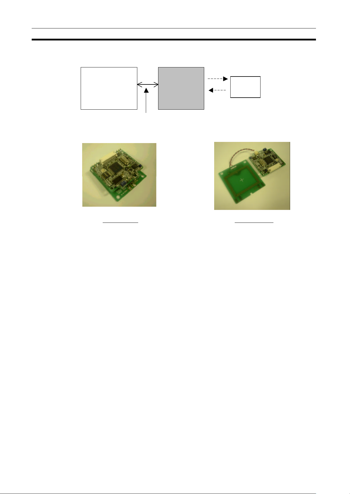
SECTION 1
Product Outline
The R/W Module is designed to be combined with other devices, and is configured from an antenna PCB and a
control PCB equipped with control functions and send-receive functions for communicating with OMRON
V720-series Tags, which use two types of Phillips Semiconductor I-CODE chips (product name: SL1 ICS30 01,
commonly known as "I-CODE1", and product name: SL2 ICS20, commonly known as I-CODE2). The SL2
ICS20 chip fully conforms to ISO/IEC15693.
The V720S -HMC73 combines the control PCB and the antenna PCB in a compact Unit. The V720S-HMC73T
provides the control PCB and the antenna PCB separately, and can be used in locations where mounting space
is restricted. The V720S-HMC73T control PCB and antenna PCB are connected via a connector.
1-1 Features..........................................................................................................1-2
1-1
Features Section 1-1
V720 series
Cable with housing
1-1 Features
Control
Unit
(Host control unit)
Compact, Low Power Consumption
V700-A30 (manufactured by OMRON, sold separately)
V720S-HMC73 V720S-HMC73T
• 40 x 44 x t14mm (V720S -HMC73)
• Operating: 5 V 70 mA, 90 mA (when the tag is contact with the antenna)
Reader/Writer
Module
V720S-HMC73
V720S-HMC73T
Tag
Slim (V720S -HMC73T)
• Max. width: approx. 10 mm (V720S-HMC73T control PCB)
Select Baud Rate and Communications Control Method to perform communications with the Host
Control Unit
• Select 9,600 bps or 38,400 bps baud rate.
• Select CR control or number -of-characters control for communications
control method.
User-friendly Command Structure
• Easy-to-understand command structure
• Built-in repetitive data write command (enabled when writing identical
data to tag memory areas)
• Specify data code (hexadecimal or ASCII) using read/write command
(CR control only)
Many Operating Modes
• Supports two operating modes -- single access mode and FIFO access
mode -- according to the status of the tags within the communications
range.
• Supports four communications modes depending on the tag
communications method. (Three communications modes when using
single access mode.)
1-2

SECTION 2
Specifications and Performance
2-1 Nomenclature and Descriptions .....................................................................2-2
2-2 Specifications.................................................................................................2-3
2-2-1 General Specifications ...................................................................................2-3
2-2-2 Interface Specifications ..................................................................................2-4
2-2-3 Interface Electrical Specifications ....................................................................2-5
2-2-4 Interface Circuit .............................................................................................2-6
2-3 Dimensions.....................................................................................................2-7
2-4 Antenna Center Position .................................................................................2-8
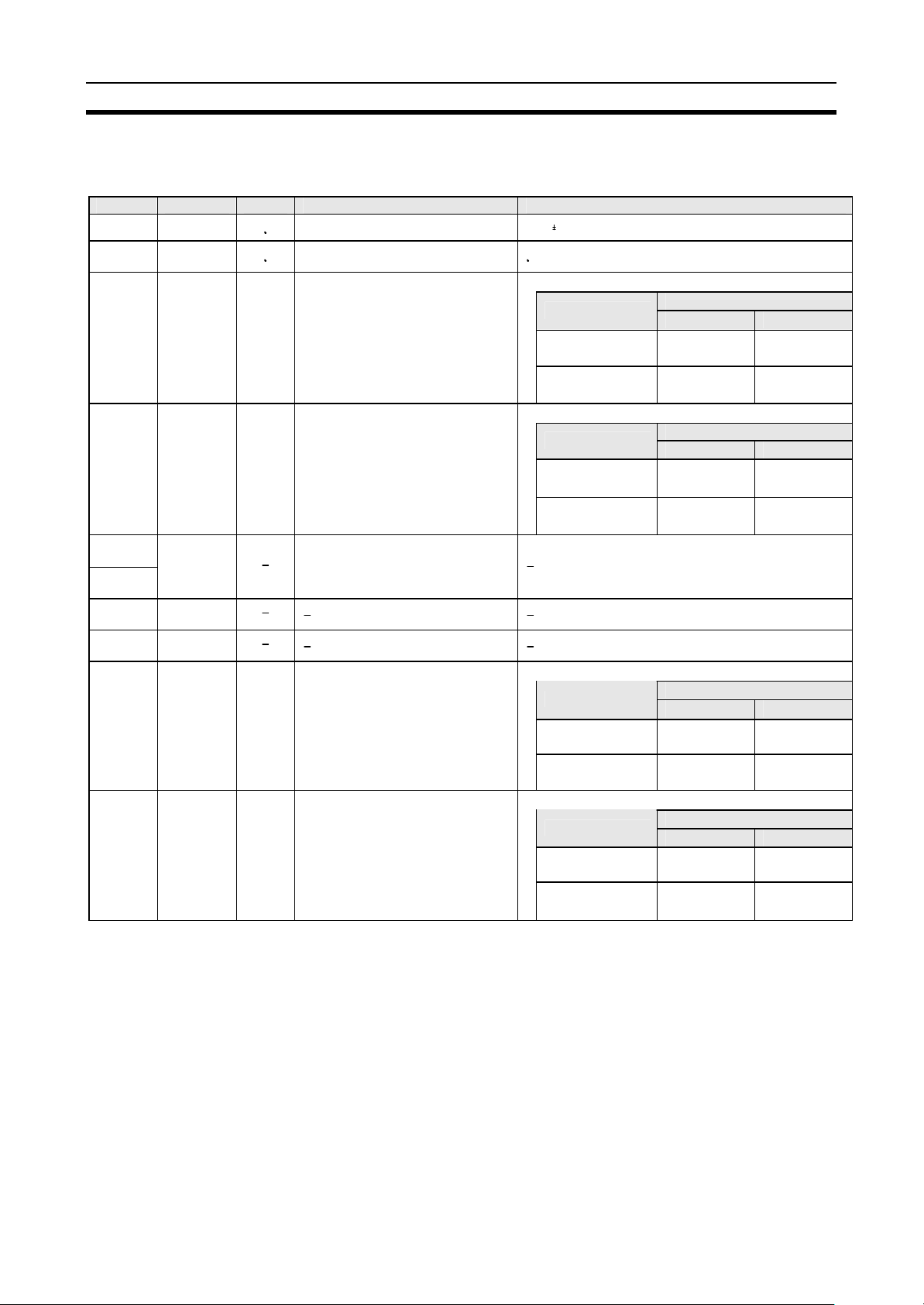
2-1
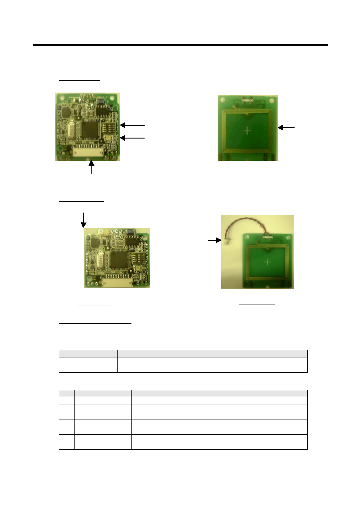
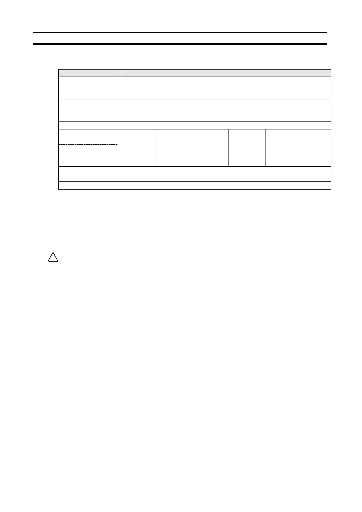
Nomenclature and Descriptions
Mode Switch
LED
Host Interface Connector
Antenna
PCB con
nector (female)
PCB
Control PCB
Antenna PCB
2-1 Nomenclature and Descriptions
V720S-HMC73
Indicator
V720S-HMC73T
Component Descriptions
•LED Indicator
The LED indicator lights up to show the R/W Module operating status.
Color Details
Green
Red
Lit during communications with the tags.
Lit when communications cannot be completed normally.
•Mode Switch
Set the R/W Module operating status using the DIP switch.
No. Name Details
1
Baud rate setting OFF: 9,600 bps ON: 38,400 bps
Communications
2
control mode setting
Reserved for system
3
use
Reserved for system
4
use
OFF: CR control ON: Number-of-characters Control
Always OFF.
Always OFF.
Note All pins are turned OFF at the factory. Change the settings to those required for the user
application.
connector
(male)
Section 2-1
(+ shows center
of antenna
surface)
2-2

Specifications
• Host Interface Connector
Use this connector to connect to the host control unit.
• Antenna
Move the tags close to the antenna when communicating with the tags.
• PCB Connectors (V720S -HMC73T)
Use these connectors to connect the control PCB to the antenna PCB.
!
Caution The PCB and antenna connector is removed for the V720S-HMC73T at the factory. Be sure
to connect the control PCB and antenna PCB before turning ON the power supply.
2-2 Specifications
2-2-1 General Specifications
Item V720S-HMC73 V720S-HMC73T
Dimensions 40 × 44 × 14 mm (thickness)
Mounting method 3 x M2.3 screws
Power supply voltage 5 VDC 10%
Approx. 90 mA max. (oscillating, when the tag is contact with the antenna),
Current consumption
Approx. 70 mA max. (oscillating)
Section 2-2
40 × 44 × 10 mm (thickness) (control
PCB)
40 × 44 × 2 mm (thickness) (antenna
PCB)
2 x M2 screws (control PCB)
3 x M2.3 screws (antenna PCB)
Vibration resistance
Shock resistance Destruction: 150 m/s² three times each in 6 directions
Ambient operating
temperature
Ambient storage
temperature
Ambient operating
humidity
Communications
frequency
Weight Approx. 12 g
Radio standards
*1
For the information of communications distance and area, refer to the data in 5-1 and 5-2 of section 5.
Destruction: 10 to 150 Hz, 0.1-mm half amplitude at 15 m/s² in X, Y, and Z directions 10
times each for 8 minutes
-10 to +55
-25 to +65
25% to 85% max. (with no condensation)
13.56 MHz
Extremely low power radio station (Radio Law Article 4 Section 1 radio stations that
discharge extremely low electric waves and specified by the Ministry of Posts and
Telecommunications ) In accorda nce with Radio Law enforcement regulation Article 6
Section 1, the field intensity is 500µV/m or less at distance of 3 m (322 MHz or less).
2-3
Specifications
Section 2-2
2-2-2 Interface Specifications
Item Details
Connectors
Communications
method
Synchronous method Asynchronous mode or start-stop synchronous mode
Communications
control method
Baud rate
Character format
1) CR control
2)
Number-of-characters
control
Error detection
method
*2
To connect the R/W Module, use an OMRON V700-A30 Connecting Cable (sold separately), or perform
Bit send order Least significant bit (LSB) first
wiring using the following housing and contacts.
• Housing: ZHR-10 (JST Manufacturing Co., Ltd.)
• Contacts: SZH-002T-P0.5 (JST Manufacturing Co., Ltd.), applicable wire sizes: AWG28 to
AWG26
SZH-003T-P0.5 (JST Manufacturing Co., Ltd.), applicable wire sizes: AWG32 to AWG28
Caution Use as short a connecting cable as possible (300 mm max.) to reduce noise.
!
*3
Set using the DIP switch.
*2
*3
*3
S10B-ZR-SM3A -TF (JST Manufacturing Co., Ltd.)
2-wire half duplex serial (CMOS level)
CR control/Number-of-characters control
9,600 bps / 38,400 bps
Start bits Data bits Parity Stop bits Total bits
1 8 Even 1 11
1 8 None 1 10
Parity (CR control) or BCC (number-of-characters control)
2-4
Specifications
2-2-3 Interface Electrical Specifications
Pin No. Symbol I/O Function Electrical characteristics
1 Vcc 5 V power supply 5 V 10%
2 GND Ground
CMOS input with 47 kΩ pull-up, positive logic
Specified value
Min. Max.
Vcc x 0. 7 Vcc + 0.3 V
-0.3 V Vcc x 0. 3
Specified value
Min. Max.
Vcc - 1.0 V
(I
= -200 µA)
OH
-----
3 RxD Input
4 TxD Output
5
GND
6
Serial input
Serial output
Ground
Item
High level input
voltage
Low level input
voltage
CMOS output, positive logic
Item
High level output
voltage
Low level output
voltage
Section 2-2
-----
0.6 V
(I
= 1.6 mA)
OL
7 Reserved
8 -
Output when Module is operating
9 RUN Output
10 OSC Output
normally.
Output during antenna oscillation.
Note Do not connect unused signals.
CMOS output, positive logic
Item
High level output
voltage
Low level output
voltage
CMOS output, positive logic
Item
High level output
voltage
Low level output
voltage
Vcc - 1.0 V
(I
= 1.5 mA)
OH
Vcc - 1.0 V
(I
= -200 µA)
OH
Specified value
Min. Max.
-----
-----
Specified value
Min. Max.
-----
(I
= 1. 6 mA)
OL
(I
= 1. 6 mA)
OL
0.6 V
-----
0.6 V
2-5
Specifications
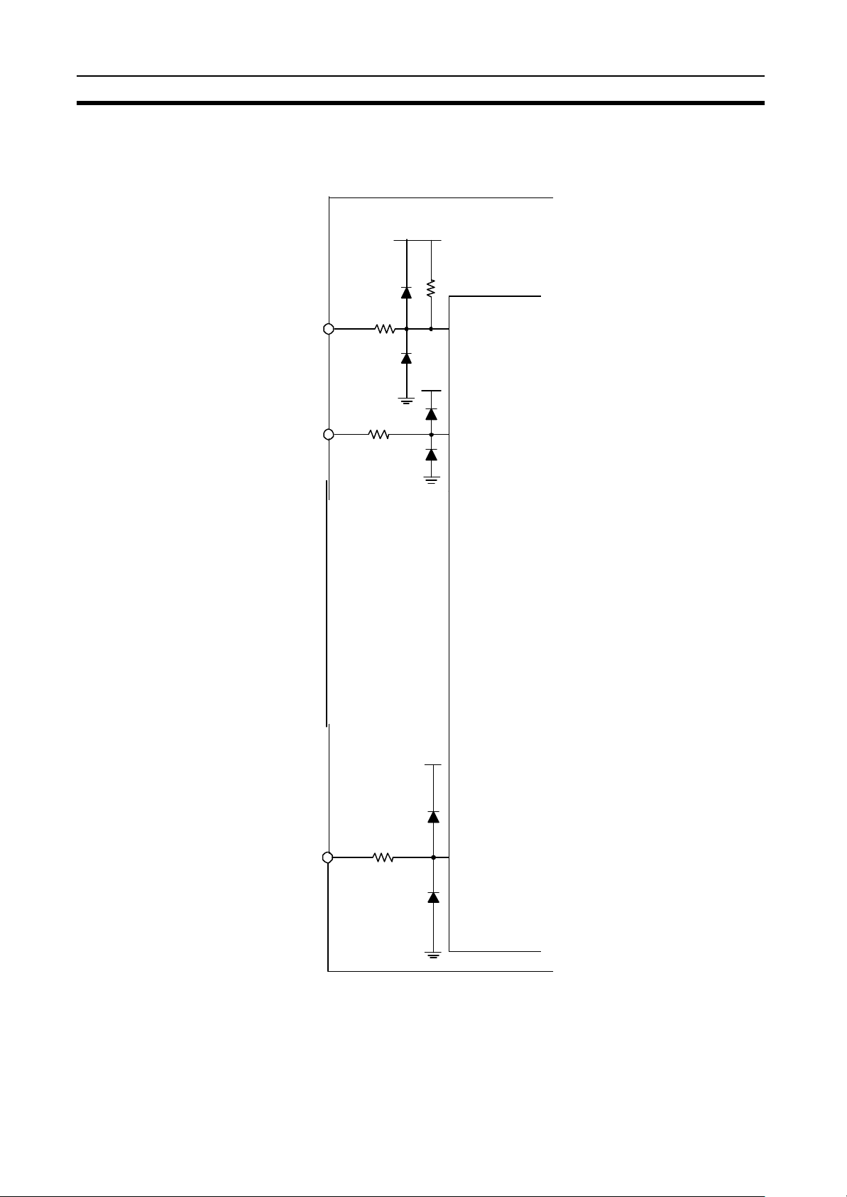
2-2-4 Interface Circuit
RxD pin No.3
TxD pin No.4
RF Module side
Vcc
47 kΩ
100 Ω
Vcc
100 Ω
Section 2-2
CPU
STOP pin No.8
RUN pin No.9• C
OSC pin No.10
100 Ω
100 Ω
Vcc
‚T‚u
‚T‚u
Vcc
Internal pull-up
2-6
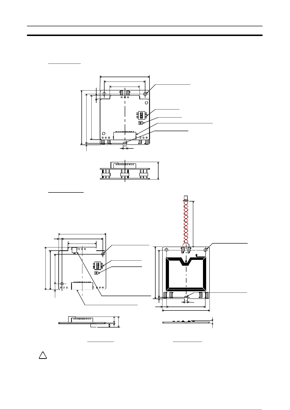
40 24
14 1 44 40 36 3
36 33 25
24
5 3 1 5 9 2 44 40
33
1
Dimensions
2-3 Dimensions
V720S-HMC73
Section 2-3
33
2.5
2-Φ2.5(Mounting Hole)
Mode Switch
LED Indicator
Connector:S10B-ZR-SM3A-TF(JST)
R1.25(Mounting Hole
)
V720S-HMC73T
3
40
34.5
2-Φ2.2(Mounting Hole)
Mode Switch
LED Indicator
Connector:SM02B-SRSS-TB(JST)
Connector:S10B-ZR-SM3A-TF(JST)
3.5
2-Φ2.5(Mounting Hole)
R1.25(Mounting Hole)
2.5
40
Control PCB Antenna PCB
Caution Use non-metal screws in the 2.2-diameter mounting holes on the V720S -HMC73T.
!
2-7
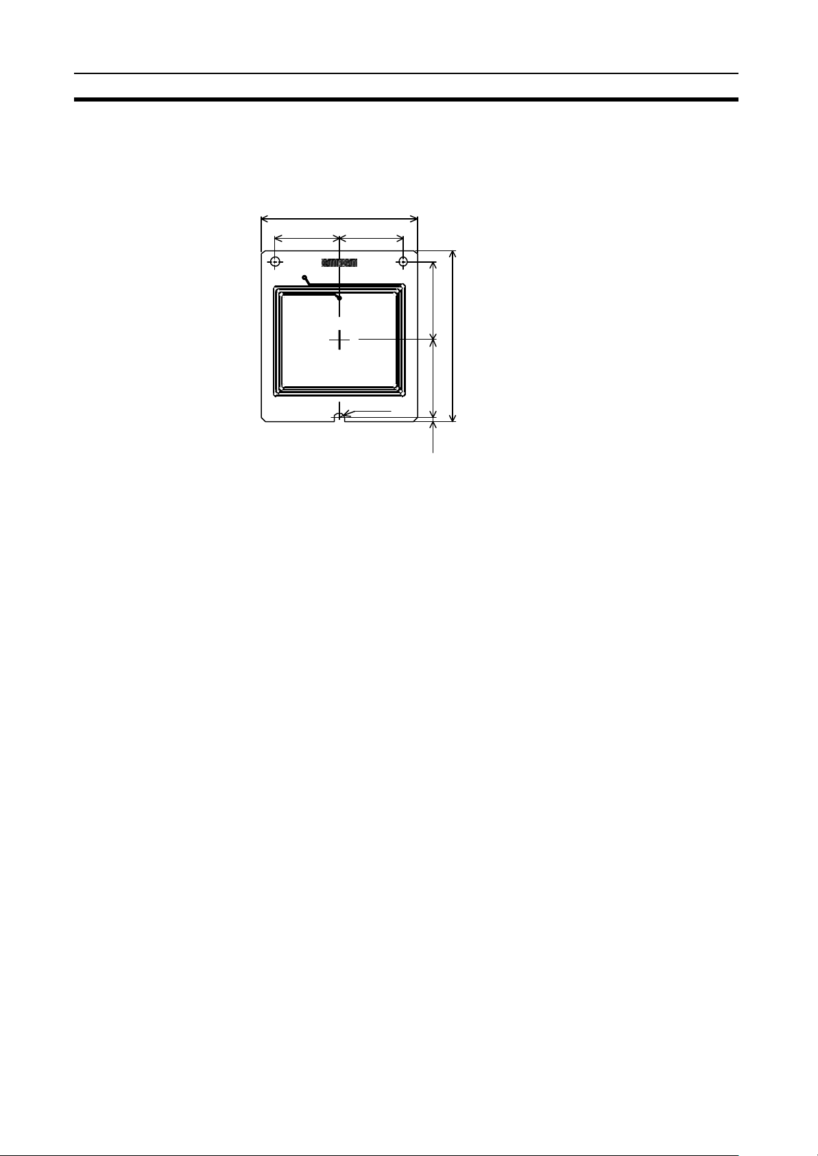
Antenna Center Position
2-4 Antenna Center Position
The center position of the antenna is shown by the silk (cross shape) on the antenna board.
Relative to the mounting hole, this cross is positioned as illustrated bel ow.
40
16.5 16.5
R 1. 25
Section 2-4
2020
44
(1)
2-8

SECTION 3
R/W Module Operations
3-1 Outline of Operations......................................................................................3-2
3-2 Tag Access Functions.....................................................................................3-3
3-2-1 Tag Memory Map...........................................................................................3-3
3-2-2 Single Access and FIFO Access Functions ......................................................3-8
3-2-3 Lock Function................................................................................................3-9
3-2-4 Tag Identification Access Function ..................................................................3-10
3-1
V720 series
Responses to
Commands from
Outline of Operations
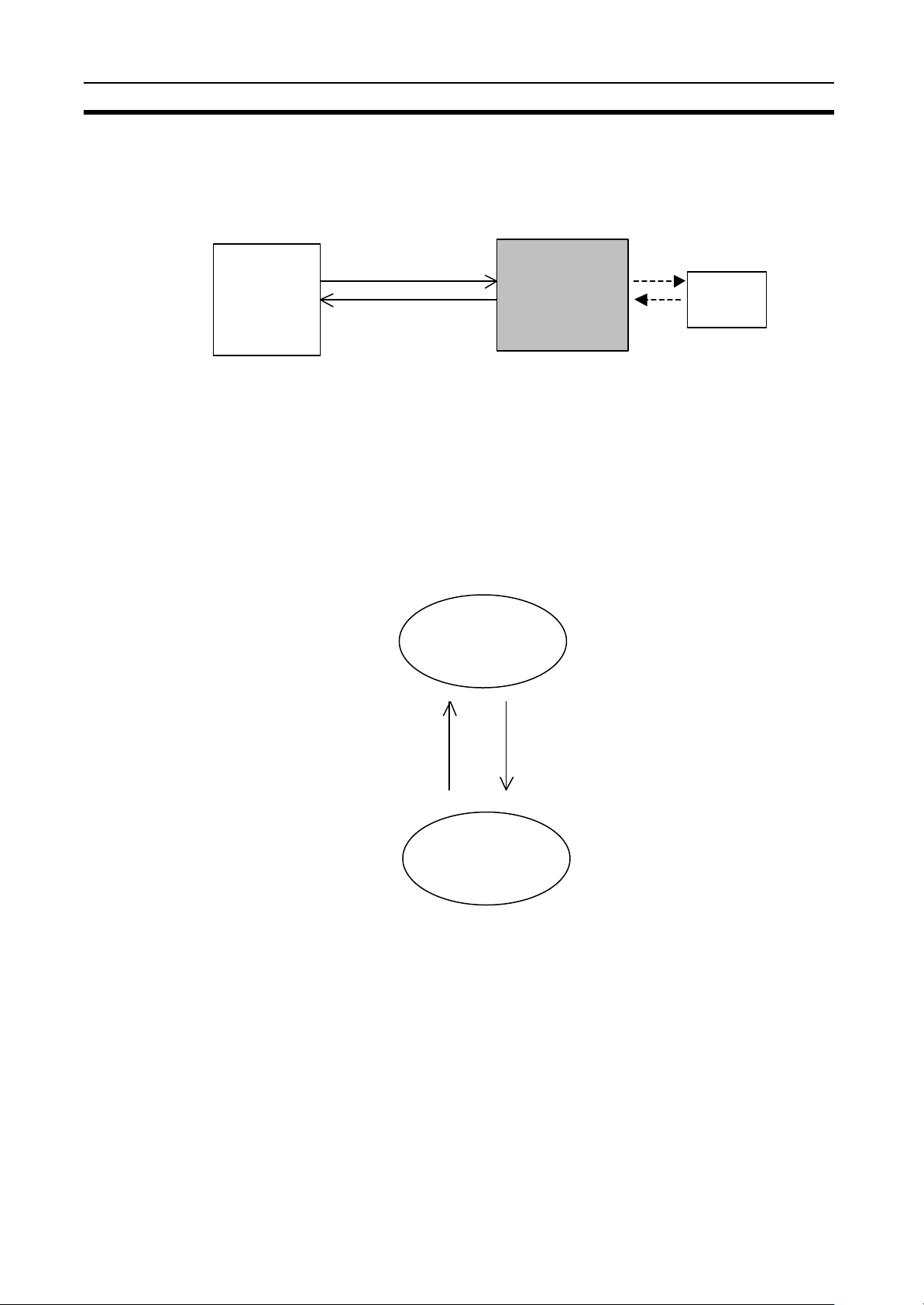
3-1 Outline of Operations
The R/W Module reads or writes to the tags using commands sent from the
host control unit, and returns the processing responses to the host control unit.
Control
Unit
The R/W Module has two operating modes. The conditions for changing the
mode are shown in the following diagram.
(1) Oscillation mode
This mode performs communications with the tags.
When using FIFO access mode, oscillation mode continues until a STOP
command.
(2) Sleep Mode (Non-oscillation Mode)
This mode waits for commands from the host control unit.
host completed
Command
Response
Reader/Writer
V720S-HMC73
V720S-HMC73T
Sleep Mode
(non-oscillation
mode)
Module
Module
host completed
Section 3-1
Tag
3-2
Oscillation mode
Tag Access Functions
Section 3-2
3-2 Tag Access Functions
3-2-1 Memory Map of Tag
3-2-1-1 I-CODE1 Chip (Philips IC product name : SL1 ICS30 01, SL1 ICS31 01)
1) Memory Map of I-CODE1
These specifications describe a Tag incorporating an IC chip I- CODE1 Label
IC from Philips, which is accessed by the system.
This chip consists of a 64-byte memory. The upper five blocks (Blocks 0 to 4)
of the memory are used as a system area having functions that do not relate to
user memory. OMRON offers special commands for accessing this area in
order to ensure the great ease of these functions by the user.
Refer to Command List for details. OMRON defines the blocks below Block 5
as the user memory area. Block 5 is page 00h, and the subsequent blocks are
allocated as shown below.
The memory is organized with four bytes as one page (4 bytes = 32 bits).
One page is the minimum unit that can be read from and written to the
memory.
The memory allocation described in this user's manual is in accordance with
OMRON's memory allocation scheme.
OMRON PHILIPS
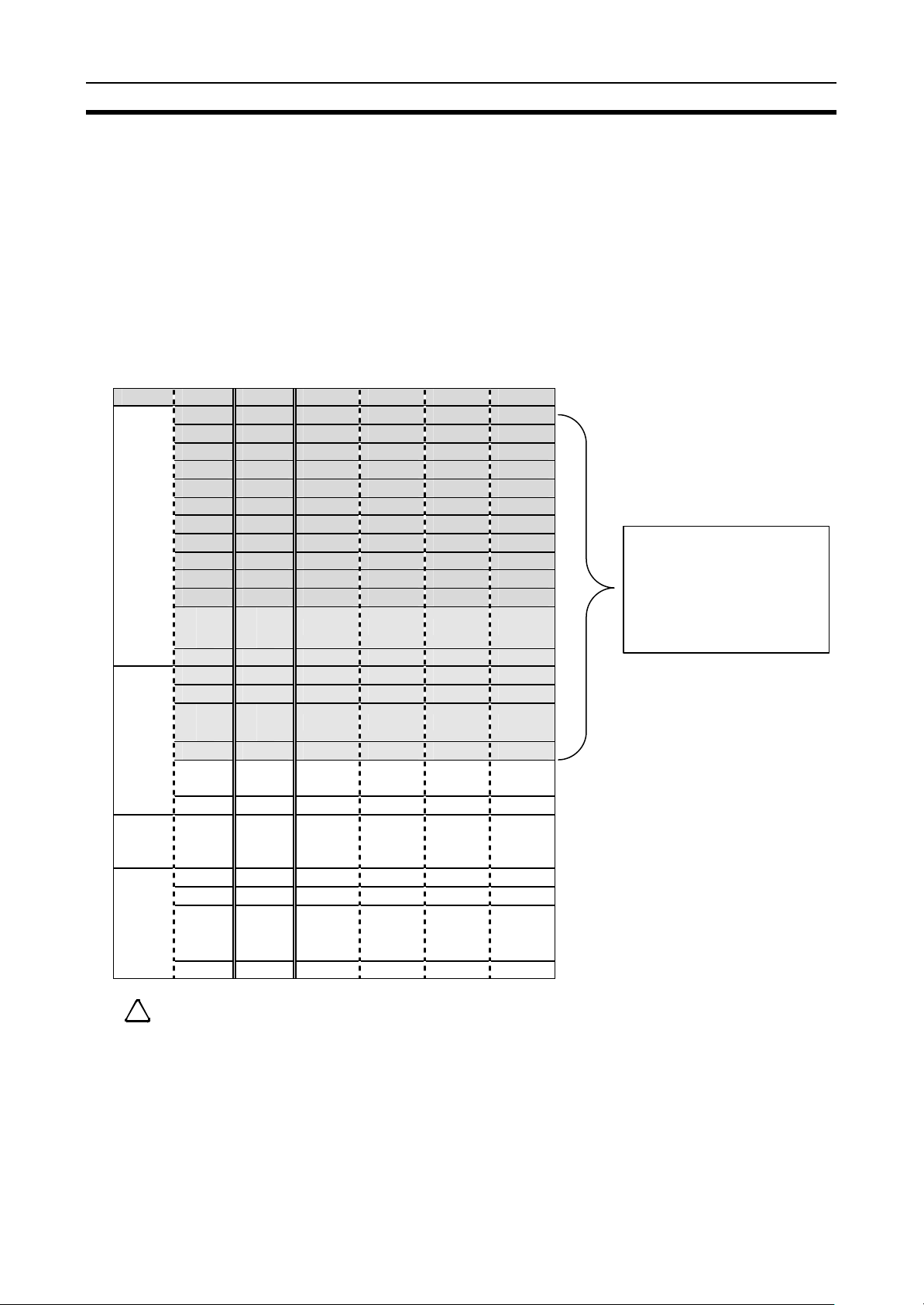
Bank Page Byte 0 Byte 1 Byte 2 Byte 3 Block
B Hex SNR 0
C Hex SNR 1
D Hex Write-protect 2
E Hex QUIET/EAS 3
F Hex Family code/application ID or user area 4
0 Hex User area 5
1 Hex 6
00 Hex 2 Hex 7
3 Hex 8
4 Hex 9
5 Hex 10
6 Hex 11
7 Hex 12
8 Hex 13
9 Hex 14
A Hex 15
Special Note Block 4 can be used as part of the user memory when the Distinguished Tag
Read/Write function by family code (FC) or application ID (A I) is not used. If such use is
preferred, define this page as F Hex to use it as part of the user memory. In this case,
the user memory area becomes 12 pages long.
3-3
Tag Access Functions
2) System Area of I-CODE1
(1) SNR pages C Hex , B Hex
(2) Write-access conditions (page D Hex )
(3) QUIET/EAS (page E Hex )
(4) Family code/application ID (page F Hex )
Section 3-2
The system area of I-CODE1 is mapped onto the memory. OMRON allocates
the system area to pages B Hex to F Hex.
SNR is a tag-specific code and has been written into the memory during the
chip production process.
The R/W Module is shipped with this page write -access inhibited (refer to page
D Hex ); there is no way of making this page rewritable by the user.
The pages are write-inhibited permanently if they are so indicated in the
memory map. The factory settings are as follow. If the two bits of a particular
page are 0.0, that page is write-protected.
Page
D Hex
Byte 0 1 1 1 1 0 0 0 0
Byte 1 1 1 1 1 1 1 1 1
Byte 2 1 1 1 1 1 1 1 1
Byte 3 1 1 1 1 1 1 1 1
QUIET mode: All the functions of a tag are suspended completely. Use Reset
Quiet Bit to resume these functions. (q=0: QUIET mode disabled; q=1: QUIET
mode enabled)
EAS mode: inhibition/permission of EAS function
(e=0: EAS mode disabled; e=1: EAS mode enabled)
Page Eh MSB LSB
Byte 0 q q e e
Byte 1
Byte 2
Byte 3
The pages marked with "×" in the table above are reserved for future use.
Family code and application ID are special areas for enabling the user to
identify an IC that is suitable to a specific user application.
Block Eh MSB LSB
Byte 0 Family code
Byte 1 Application ID
Byte 2 User area
Byte 3 User area
MSB LSB
Page E Hex Page D Hex Page C Hex Page B Hex
Page 2 Hex Page 1 Hex Page 0 Hex Page F Hex
Page 6 Hex Page 5 Hex Page 4 Hex Page 3 Hex
Page A Hex Page 9 Hex Page 8 Hex Page 7 Hex
3-4
I-CODE2
Page 00 Hex to 1B Hex
Tag Access Functions
3-2-1-2 I-CODE2 Chip (Philips IC product name : SL2 ICS20)
In this module, processing is performed with the minimum access unit of one
page (4 bytes), the maximum number of pages that can be processed
simultaneously being one bank (16 pages), and up to a total of 16 banks (266
pages) being accessible.
The I-CODE 2 user memory area spans 112 bytes, or 28 pages, from page 00
Hex to page 1B Hex.
1) Max. address space of ISO/IEC15693 chip with a 4 Bytes/page organization
Bank Page Block Byte 0 Byte 1 Byte 2 Byte 3
0 Hex 0
1 Hex 1
2 Hex 2
3 Hex
4 Hex
5 Hex
00 Hex
6 Hex
7 Hex
8 Hex
9 Hex
A Hex
…
user memory area
…
(28 pages =112 bytes)
Section 3-2
F Hex 15
0 Hex 16
1 Hex 17
01 Hex
…
B Hex 27
…
…
…
F 31
…
…
…
0 Hex 240
1 Hex 241
0F Hex
…
…
F Hex 255
!
Caution The memory map above shows a memory area covered by th e product. It complies with the
ISO/IEC15693 standard.
Proper operation is ensured for our Tag, which incorporates Philips' IC product SL2ICS20
(known as "I-CODE2"), although this product incorporates a firmware allowing to access
chips with a four bytes/page organization and fully compliant to ISO/IEC15693. Perform
check test adequately when using other company’s tag or tags that incorporate other
ISO/IEC15693 chips.
3-5

Tag Access Functions
2) System Area of I-CODE2
(1) UID
(2) EAS/AFI/DSFID
(3) AFI
Section 3-2
The I-CODE2 system area of is reserved in an area different from the user
memory.
Special commands are used for accessing the system area.
Byte 0 Byte 1 Byte 2 Byte 3
UID
UID
EAS/AFI/DSFID
Write-protect
UID is a tag-specific code and has been written into the memory during the
chip production process.
The R/ W Module is shipped with this page write-access inhibited; there is no
way of making this page rewritable by the user.
EAS mode: Inhibition/permission of EAS function
(e=0: EAS mode disabled; e=1: EAS mode enabled)
MSB LSB
Byte 1 e
The pages marked with "×" in the table above are reserved for future use.
AFI is a special area for enabling the user to identify a tag that is suitable to a
specific user application.
MSB LSB
Byte 2 AFI upper 4 bits AFI lower 4 bits
AFI upper
4 bits
0 0 All areas Area not identified
X 0 X area Selected extensively
X Y Y category of X area
0 Y Limited to Y category
1 0,Y Transportation
2 0,Y Finance Bank
3 0,Y Recognition Access control
4 0,Y Telecommunication Public telephone, CSM
5 0,Y Medical care
6 0,Y Multimedia Internet
7 0,Y Game
8 0,Y Data storage Portable file
9 0,Y Logistics
A 0,Y Home delivery services
B 0,Y Mail
C 0,Y Airplane luggage
D 0,Y Reservation
E 0,Y Reservation
F 0,Y Reservation
*Remarks: X=1 to F Y=1 to F
AFI lower
4 bits
Application area Example/reference
Mass -transit, bus, air pl ane
3-6

Tag Access Functions
(4) DSFID
(5) Write-access conditions
Section 3-2
DSFID indicates how the data is configured in the memory.
MSB LSB
Byte 3 DSFID
The pages are write-inhibited permanently if they are so indicated in the
memory map. The factory settings are as follow. If the bit of a particular page is
1, that page is write-protected.
MSB LSB
Byte 0 0 0 0 0 0 0 0 0
Page 03Page 02Page 01Page
00
Byte 1 0 0 0 0 0 0 0 0
Page 0BPage 0APage 09Page 08Page
Byte 2 0 0 0 0 0 0 0 0
Page 13Page 12Page 11Page 10Page
Byte 3 0 0 0 0 0 0 0 0
Page 1BPage 1APage 19Page 18Page
07
0F
17
Page
06
Page
0E
Page
16
Page
05
Page
0D
Page
15
Page
04
Page
0C
Page
14
3-7

Tag Access Functions
3-2-2 Single Access and FIFO Access Functions
Single Access Mode
Use this mode to communicate with only one tag within the R/W Module
communications area.
The time required for communications with the tag is shorter compared with
FIFO access mode.
FIFO Access Mode
FIFO (First In First Out) access mode enables reading tags in order as they
enter the antenna communications range. Tags with which communications
have been completed are prohibited from being accessed again, so even if
tags with which communications have been completed are still within range of
the antenna, communications will be possible with new tags as they enter the
communications range. When two or more tags enter the antenna
communications range at the same time, a communications error will occur.
When a tag to which access has been prohibited moves out of the
communications area, communications with it will be possible again if it
reenters the antenna communications range.
The above diagram shows an example of a tag inspection line.
When the distance between tags is small, two tags may enter the R/W Module
communications range at the same time. If this happens when in Single
Access Mode, a communications error will occur, or even if read/write appears
to have been performed, there is no way to know which of the two tags was
read. In FIFO Access Mode, tags entering communications range can be read
or written to in order, so this mode is suited to applications such as a tag
inspection line, in which the order of access is important.
Section 3-2
3-8

Tag Access Functions
3-2-3 Lock Function
Note The lock function used with the V720 Series cannot be canceled. Pages that have been
write-protected cannot be written to again, so be careful when using this function.
Section 3-2
The lock function is a protection function provided to prevent the loss of data
by unintentionally overwriting fixed data stored on the tags. This function can
be set using the lock command. This function can be set using the lock
command.
There is a lock setting area in the tag system area, enabling user-defined
areas to be write-protected one page at a time. If the write command is
executed for a page that has been write-protected, a write processing error will
occur.
3-9

1 2 3
1 2 3
Section 0
3-2-4 Tag Identification Access Function
Only when the ID code stored on the tag and the ID code included in the
command sent from the antenna match will the tag respond. This is called the
tag identification access function.
Commands sent from the R/W Module respond without depending upon the ID
code stored in the tags.
Reference Information for I-CODE1
An example of using tag ID access using OMRON V720-H01 R/W Antenna and V720-CD1D is given
below.
(1) The set values of the tag ID codes are given in the following table. These settings can be made using the
R/W Module or the combined R/W Antenna and ID Controller.
Tag No.1 Tag No.2 Tag No.3
Family Code
Application ID
(2) Tag ID Access Operation
•Not Using Tag ID Access
•Using Tag ID Access
55 Hex 55 Hex 00 Hex
AA Hex 11 Hex 00 Hex
(1) Both the ID Controller family code and the application ID
set value are taken to be 00 Hex. (Set at the factory.)
(2) Multiple tag access commands are executed.
(3) All tags within communications range respond.
(The tag family codes and application IDs are not
required.)
(1) The set value of the ID Controller family code is 55 Hex,
and the application ID is 11 Hex.
(2) Multiple tag access commands are executed.
(3) Only tags with the same ID code set in (1) and which are
within communications range respond. In this exam ple,
only tag No. 2 responds.
3-10

SECTION 4
Controlling the R/W Module
Two methods of controlling the R/W Module from the host control unit are possible: CR control and
number-of-characters control.
CR control
Number-of-ch
aracters
Control
In this manual, the codes are displayed as follows:
ASCII characters: ’ ×× ‘
Control code using ASCII characters: ‘<Control code>‘
Displayed as hexadecimal code: ×× Hex
4-1 Communications Frames........................................4-2
4-1-1 CR Control 4-2
4-1-2 Number-of-characters Control 4-2
4-2 Data Formats .................................................4-3
4-2-1 Command Code List 4-3
4-2-2 Communications Options 4-5
4-2-3 End Code List 4-9
4-3 Commands and Responses during CR Control.......................4-10
4-3-1 General Commands (Commands sent to RF Module) 4-10
4-3-2 Commands Common to the I-CODE1 and the I-CODE2 Chips 4-11
4-3-3 Commands Specific to the I-CODE2 Chip 4-15
4-3-4 Commands Specific to the I-CODE1 Chip 4-18
4-3-5 Old Commands Specific to the I-CODE1 Chip 4-20
4-4 Commands and Responses during Number-of-characters Control ........4-24
4-4-1 General Commands (Commands sent to the RF Module) 4-24
4-4-2 Commands Common to the I-CODE1 and the I-CODE2 Chips 4-25
4-4-3 Commands Specific to the I-CODE2 Chip 4-29
4-4-4 Commands Specific to the I-CODE1 Chip 4-32
4-4-5 Old Commands Specific to the I-CODE1 Chip 4-34
Data in the communications frame is handled as ASCII characters in 2-digit hexadecimal code
(ASCII code). CR control simplifies operations with the host.
Data in the communications frame is handled as hexadecimal code, thus minimizing
communications time with the host.
4-1

Communications Frames
bit data taking the exclusive logical sum (ExOR) of the number of
4-1 Communications Frames
4-1-1 CR control
The frame format consists of data in ASCII characters and a terminator. '<CR>' (ASCII: 0D Hex), the
terminator, cannot be used in the data ASCII characters.
The CR control method is useful when the R/W Module is connected to a PC and the like.
Data 1 Data 2 ⋅⋅⋅⋅⋅⋅ Data n Terminator
Data: 138 characters max
Section 4-1
Data
Data
Terminator
No. of
characters
1 to 138
1
Command parameters (ASCII characters)
Code ‘<CR>‘ (0D Hex), which indicates end of communications
frame
(Communications Control Procedure)
When a character is first received, reception starts, and when <CR> is received, the frame ends. If the
interval between data is greater than 2 sec, a communications error occurs. If a communications error
occurs, a frame error end code (Error code: '18') is sent as the response from the R/W Module to the
host.
4-1-2 Number- of-characters Control
The frame format is given below, with ‘<STX>‘ (ASCII code: 02 Hex) as the beginning of the frame.
The number -of-characters control method is useful when the R/W Module is directly connected to a
microcomputer board, allowing communications time with the host device to be reduced.
STX
Data
STX 1
No. of
characters
Data 1 69
BCC 1
No. of
characters
No. of
characters
1
Data 1 Data 2 ⋅⋅⋅⋅⋅⋅ Data n BCC
Code indicating start of communications frame (02 Hex).
Total number of data and BCC characters in hexadecimal.
Command parameters (hexadecimal)
8characters and the data characters
(excluding STX).
Example: Using STX 03 10 00 BCC
(Communications Control Procedure)
When character data has been received for the number of characters given at the beginning of the
frame, the frame is assumed to have ended. If the interval between data is greater than 2 sec,
processing of the reception is interrupted, and the sleep mode is engaged. If reception is stopped,
responses are not returned from the R/W Module to the host.
Data: 69 characters max
BCC = (03 Hex) ExOR (10 Hex) ExOR (00 Hex) = 13 Hex
Details
Details
4-2

Data Formats
4-2 Data Formats
The data in the communications frames used for commands and responses use the following formats.
n Command
The command data consists of the command, communications options, and parameters. The
communications options are added only to commands 01 to 03.
Command
n Response
The response data consists of an end code and parameters.
End code Parameter 1 ⋅⋅⋅⋅⋅⋅ Parameter n
4-2-1 Command Code List
Commands specify R/W Module processing. The commands are given in the following table.
1) General Commands (Commands sent to the RF Module)
Command name No. Details
Test 10
ACK 11
NACK 12
STOP 13
Communications
option
Sends the received data to the host device.
The host device received the data properly.
The host device did not receive the data properly.
Ends the command currently being executed.
Stops antenna oscillation.
Parameter 1 ⋅⋅⋅⋅⋅⋅ Parameter n
Section 4-2
2) Commands Common to the I-CODE1 and the I-CODE2 Chips
Command name No. Details
Read 31
Write 32
Write identical data 33
Read UID (SNR) 35
Set write-protection 39
Reads tag memory data on a page basis.
Writes data to tag memory on a page basis.
Writes identical data to tag memory on a page basis.
Reads tag serial numbers.
Sets write-protection on a page basis
3) Commands Specific to the I-CODE2 Chip
Command name No. Details
Set AFI
Set DSFID
Read Tag info 3A
Read UID & data
EAS Alarm
Set EAS
Overwrites and locks tag AFI.
Overwrites and locks tag DSFID.
Reads tag system information.
Reads tag UID and memory data simultaneously.
Sends EAS Alarm to the tag.
Enables/disables and locks EAS.
4) Commands Specific to the I-CODE1 Chip
Command name No. Details
Read SNR 05
Read Family
Code and
Application ID
Set Family Code
and Application ID
Set EAS 08
EAS 24
06
07
Reads tag serial numbers.
Reads tag family codes and application IDs.
Writes tag family codes and application IDs.
Permits/prohibits EAS commands to the tags.
Sends EAS commands to the tags.
4-3

Data Formats
5) Old Commands Specific to the I-CODE1 Chip (replaced by the Commands Common to the I-CODE1
and the I-CODE2 Chips)
Command name No. Details
Read Reads tag memory data on a page basis.
Write Writes data to tag memory on a page basis.
Write identical data Writes identical data to tag memory on a page basis.
Set write-protection Sets write-protection on a page basis.
Note These commands support the commands that are specific to I-CODE1 in the old RF module
(V720-HMC73 and 73T).
Section 4-2
4-4

Data Formats
4-2-2 Communications Options
The data code and communications mode can be specified as communications options. Data code
specification is possible only when using CR control.
Bit 7 6 5 4 3 2 1 0
Setting
details
*Bits 6 and 7 must be 0.
1) Specifying Tag Type
Setting Value Details
I CODE1 0
ISO/IEC15693
(4byte/page type)
2) Specifying Data Code
n Using CR Control
Specify the data code to perform read/write communications between the R/W Module and the host
control unit. The specification concerns the data to be written/read to/from the user memory, as well
as the test data.
Setting
Val
ue
1
Tag type
When accessing a tag equipped with I-CODE1
When accessing a tag equipped with I-CODE2
Addendum: when accessing the tag equipped with a chip with a
four bytes/page organization and fully conforming to
ISO/IEC15693
Data
code
Section 4-2
Communications mode
Details
Hex 0
ASCII 1
Two-character data consisting of 0 to 9 and A to F is handled as 2-digit
hexadecimal data. Two characters occupy one byte of tag memory.
Example: When 12345678 is written to page 0, tag memory is used as
shown below.
Page 0
One character of data occupies one byte of tag memory as ASCII or JIS8
unit code.
Example: When ‘ABCD’ is written to page 0, tag memory is used as shown
below.
Byte 0 12
Byte 1 34
Byte 2 56
Byte 3 78
Byte 0 41
Byte 1 42
Byte 2 43
Byte 3 44
n Using Number-of-characters Control
Only hexadecimal is handled; therefore, the data code must always be set to 0.
4-5

Data Formats
3) Specifying the Communications Mode
The following seven communications modes are supported for different processing procedures and
execution timing.
Communicatio
ns mode
Single Trigger
Single Auto
Single Repeat
FIFO Trigger
FIFO Auto
FIFO
Continuous
No. Details
After a command is received, communications with the tag is performed immediately
0 Hex
1 Hex
2 Hex
8 Hex
9 Hex
A Hex
and a response is sent. If there is no tag in communications range, a No Tag error is
sent. After the response has been sent, the mode changes to sleep mode.
Only one tag is permitted in communications range.
After a command is received, this mode waits for a tag to enter communications
range, and then performs communications with the tag. After the response has
been sent, the mode changes to sleep mode. If a STOP command is received
while waiting for a tag, the command is ended.
Only one tag is permitted in communications range.
After a command is received, this mode waits for a tag to enter communications
range, and then performs communications with the tag. If this mode has been
specified, the command is repeated sequentially until a STOP command is
received. This mode is enabled only for read commands.
Only one tag is permitted in communications range.
After a command is received, communications with the tag is performed
immediately and a response is sent. If there is no tag in communications range, a
No Tag error is sent. Access is prohibited to tags with which communications
have been completed, and the R/W Module continues unmodulated oscillation.
Tags with which commu nications have been completed do not respond to the
next command. After the response has been sent, the mode changes to sleep
mode. If a STOP command is received, oscillation stops.
After a command is received, this mode waits for a tag to enter communications range,
and then performs communications with the tag. Access is prohibited to tags with which
communications have been completed, and the R/W Module continues unmodulated
oscillation. Tags with which communications have been completed do not respond to
the next command. After the response has been sent, the mode changes to sleep
mode. If a STOP command is received while waiting for a tag, the command is ended.
After a command is received, this mode waits for a tag to enter communications range,
and then performs communications with the tag. Access is prohibited to tags with which
communications have been completed, and the R/W Module continues unmodulated
oscillation. Tags with which communications have been completed do not respond to
the next command. After the response has been sent, when ACK is received, this mode
again waits for a tag to enter communications range, and then performs
communications with the tag. If a STOP command is received while waiting for a tag,
the command is ended.
Section 4-2
After a command is received, this mode waits for a tag to enter communications range,
and then performs communications with the tag. Access is prohibited to tags with which
FIFO Repeat
B Hex
communications have been completed. Tags with which communications have been
completed do not respond to the next command. If this mode has been specified, the
command is repeated sequentially until a STOP command is received.
Note Single repeat mode can only be specified for commands 01, 31, 35, 3A, 41, and 42.
4-6

Host control unit to
R/W Module to host
Communications with tag
Tag operation
tag 1
Command processing
Command processing
tag 1 Tag detection
Host control unit to
R/W Module to host
Communications with tag
Tag operation
processing
tag 1
tag 2
tag 3
Host control unit to
R/W Module to host
Communications with tag
Tag operation
Tag detection
tection
Tag detection
processing
processing
processing
Data Formats
4) Communications Modes Diagrams
1) Single Trigger
n Operation Sequence
R/W Module
control unit
2) Single Auto
n Operation Sequence
command
R/W Module
control unit
3) Single Repeat
command
response1
Command
response1
command
command
response2
No Tag Error
stop
Tag detection
Section 4-2
response
End processing
n Operation Sequence
R/W Module
command
control unit
Command
response1
Tag de
Command
response2
Tag
detection
Command
response3
stop
response
End processing
4-7

tag 1
Host control unit to
R/W Module to host
Communications with tag
Tag operation
processing
processing
tag 1
Host control unit to
R/W Module to host
Communications with tag
Tag operation
processing
tag 1
tag 2
Host control unit to
R/W Module to host
Communications with tag
Tag operation
processing
processing
tag 1
tag 2
tag 3
Host control unit to
R/W Module to host
Communications with tag
Tag operation
processing
processing
processing
Data Formats
4) FIFO Trigger
n Operation Sequence
command
R/W Module
control unit
5) FIFO Auto
n Operation Sequence
R/W Module
control unit
6) FIFO Continuous
command
Command
Tag
detection
response1
Unmodulated
oscillation
Command
response1
Unmodulated
oscillation
command
Command
command
response2
No Tag Error
Tag
detection
Section 4-2
Unmodulated
oscillation
stop
response
End processing
n Operation Sequence
R/W Module
control unit
7) FIFO Repeat
n Operation Sequence
R/W Module
control unit
command
command
Tag
detection
Tag
detection
Command
Command
response1
Unmodulated
oscillation
response1
detection
Tag
ACK
Tag
detection
Command
Command
response2
Tag
detection
response2
Command
NACK
response2
Unmodulated
oscillation
response3
detection
Tag
stop
response
End processing
stop
response
End processing
4-8

Interference, such as noise, has occurred during communications with
There was no tag in the communications area when the command was
Data Formats
4-2-3 End Code List
n Communications between Host Device and R/W Module
End code Name Details
10
11
12
13
14
18
n Communications between R/W Module and Tags
End code Name Details
70
71
72
79
7A
Parity Error
Framing Error • There is a character with a framing error in the command received.
Overrun Error • There is a character with an overrun error in the command received.
BCC Error
Format Error
Frame Error
Communications Error
Write Error
No Tag Error
Command Error • (see Comparison with ISO Error Code)
Address Error • The specified pages do not exist.
Section 4-2
• There is a character with a parity error in the command received.
(CR control only).
• The BCC for the frame received is invalid (number-of-characters
control only).
• Command format does not match specifications.
Examples: Command is not defined, page/address specifications are
invalid, etc.
• Characters are received more than 2 sec apart (CR control only).
• Frame received exceeds 140 (CR control only).
• Frame received exceeds 73 bytes (number-of-characters control
only).
•
the tags, preventing normal completion.
• Write command has been specified to a page that has been
write-prohibited.
• There is a tag area to which reading is possible, but writing is not possible.
• Correct data cannot be written because the tag has exceeded its
usable write life.
•
executed.
• The specified pages do not exist (I-CODE2).
n Comparison with ISO Error Code
When an ISO tag responds by returning an error, the module responds with the end code shown in
the following table.
ISO code Details Module end code
01
02
03
0F
10
11
12
13
14
Others
Command not in use. Cannot recognize request command code.
Unrecognized command. Example: format error
Any unused command.
Unknown or unused error code.
Specified block cannot be used (not present).
Specified block cannot be re-locked because it has been already locked.
The contents of the specified block cannot be changed because it is locked.
Writing to the specified block did not end normally.
Locking of the specified block did not end normally.
RFU
79
79
79
79
7A
00
71
71
71
79
4-9

Commands and Responses during CR Control
4-3 Commands and Responses during CR Control
4-3-1 General Commands (Commands sent to the RF Module)
1) Test
This command tests communications with the host. When this command is received, the R/W Module
sends the same data to the host.
n Command
Command Test data
‘ 1 ‘ ‘ 0 ‘ Data 1 ⋅⋅⋅⋅⋅⋅ Data n
n Response
End code Test data
‘ 0 ‘ ‘ 0 ‘ Data 1 ⋅⋅⋅⋅⋅⋅ Data n
The test data returned is the same as the command data.
2) ACK
Use this command when the communications mode is FIFO Continuous Mode.
ACK is sent after the response has been received, and the next read operation is permitted.
Section 4-3
n Command
n Response
3) NACK
n Command
n Response
4) STOP
Command
‘ 1 ‘ ‘ 1 ‘
There is no response to ACK.
If the host control unit does not receive a response normally, NACK is sent as a request to resend the
response.
When the R/W Module receives the NACK command, it resends the immediately preceding response.
Command
‘ 1 ‘ ‘ 2 ‘
The immediately preceding response data is resent.
Use this comman d to stop the R/W Module processing. When this command is received, the R/W
Module stops processing the current command and enters sleep mode. If the antenna is oscillating,
the oscillation also stops.
n Command
Command
‘ 1 ‘ ‘ 3 ‘
n Response
End code
‘ 0 ‘ ‘ 0 ‘
4-10

Commands and Responses during CR Control
Section 4-3
4-3-2 Commands Common to the I-CODE1 and the I-CODE2 Chips
1) Read
Use this command to read data from the tags. Data can be read from a user-specified page.
n Command
This command sends the pages to be read as command parameters. The page specification is as follows:
The bits that correspond to the pages to be read are set to 1, and all other bits are set to 0. This binary
number is converted to hexadecimal and sent with the command. The pages are specified by the user.
Command Communic
ations
option
‘ 3‘ ‘ 1 ‘
Bank
Tag type
I-CODE1 ‘ 00 ‘ ‘00’ to ‘FF’ ‘00’ to ‘FF’
ISO chip ‘00’ to ‘0F’ ‘00’ to ‘FF’ ‘00’ to ‘FF’
specification
(Settable value)
Bank
specificatio
n
F E D C B A 9 8 7 6 5 4 3 2 1 0
Page specification
Page specification (settable value)
n Response
Returns the data read and the end code (normal end: ‘00’). The read data is returned sequentially in
ascending order of the pages specified. If an error occurs, an error code is returned. In the case of a
Tag equipped with I-CODE1, the read data is returned in the order: B⇒C⇒ D⇒E⇒F⇒0⇒1⇒···⇒A.
End code Read data
‘ 0 ‘ ‘ 0 ‘ Data 1 Data n
*1
Number of data n = Number of specified pages x 8 (hexadecimal)
*1
Number of data n = Number of specified pages x 4 (ASCII)
Command Example
The following table gives the tag user memory details for the following example of commands and responses.
Page Byte 0 Byte 1 Byte 2 Byte 3
0 30 Hex 31 Hex 32 Hex 33 Hex
1 34 Hex 35 Hex 36 Hex 37 Hex
2 38 Hex 39 Hex 30 Hex 30 Hex
3 40 Hex 41 Hex 42 Hex 43 Hex
4 44 Hex 45 Hex 46 Hex 47 Hex
5 48 Hex 49 Hex 4A Hex 4B Hex
6 4C Hex 4D Hex 4E Hex 4F Hex
7 50 Hex 51 Hex 52 Hex 53 Hex
8 54 Hex 55 Hex 56 Hex 57 Hex
9 58 Hex 59 Hex 5A Hex 61 Hex
10 62 Hex 63 Hex 64 Hex 65 Hex
(1) Reading the following four pages: 1, 3, 5, and 6, using Single Trigger Mode with hexadecimal is
as follows:
Command ‘01 00 006A<CR>‘
Response ‘00 34353637 40414243 48494A4B 4C4D4E4F<CR>‘
(2) Reading the following four pages: 1, 3, 5, and 6, using Single Trigger Mode with ASCII is as
follows:
Command ‘01 10 006A<CR>‘
Response ‘00 4567 @ABC HIJK LMNO<CR>‘
4-11

Commands and Responses during CR Control
2) Write
Use this command to write tag data on a page basis. Data can be written to user-specified pages
(except B Hex to E Hex for I-CODE1). The maximum number of pages which can be written to in a
single operation is one bank, and writing to pages across banks is impossible. There is no need to
perform the verify read process, since this command performs it as part of its execution.
n Command
This command sends the data to be written as parameters. The page specification is as follows: The
bits that correspond to the pages to be written are set to 1, and all other bits are set to 0. This binary
number is converted to hexadecimal and sent with the command. Specify the write data sequentially
in ascending order of the specified page. In the case of a Tag equipped with I-CODE1, specify the
write data in the order: F⇒0⇒ 1⇒···⇒A.
Communic
Command
‘ 3‘ ‘ 2 ‘ Data 1 Data n
Tag type
I-CODE1 ‘ 00 ‘ 0 0 0 0
ations
option
Bank
specification
(Settable
value)
Bank
specification
F E D C B A 9 8 7 6 5 4 3 2 1 0
Page
specification
Page specification (settable value)
Write data
Section 4-3
*1
ISO chip ‘00’ to ‘0F’ ‘00’ to ‘FF’ ‘00’ to ‘FF’
*1
Number of data n = Number of specified pages x 8 (hexadecimal)
Number of data n = Number of specified pages x 4 (ASCII)
n Response
The response returns the end code (normal end: ‘00’).
End code
‘ 0 ‘ ‘ 0 ‘
Command Example
The following table gives details of tag user memory when executing the following command.
Page Byte 0 Byte 1 Byte 2 Byte 3
0 30 Hex 31 Hex 32 Hex 33 Hex
1 34 Hex 35 Hex 36 Hex 37 Hex
2 38 Hex 39 Hex 30 Hex 30 Hex
3 40 Hex 41 Hex 42 Hex 43 Hex
4 44 Hex 45 Hex 46 Hex 47 Hex
5 48 Hex 49 Hex 4A Hex 4B Hex
6 4C Hex 4D Hex 4E Hex 4F Hex
7 50 Hex 51 Hex 52 Hex 53 Hex
8 52 Hex 46 Hex 49 Hex 44 Hex
9 58 Hex 59 Hex 5A Hex 61 Hex
10 56 Hex 37 Hex 32 Hex 30 Hex
(1) Writing 52464944 hexadecimal to page 8, and 56373230 hexadecimal to page 10 using FIFO
Repeat Mode, with hexadecimal:
Command ‘02 0B 0500 52464944 56373230<CR>‘
Response ‘00<CR>
(2) Writing ‘RFID’ hexadecimal to page 8, and ‘V720’ hexadecimal to page 10 using FIFO Repeat
Mode, with ASCII:
Command ‘02 1B 0500 RFID V720<CR>‘
Response ‘00<CR>‘
Data written to tag memory is the same for both (1) and (2).
4-12

Commands and Responses during CR Control
3) Write identical data
Use this command to write identical data to tags by the page. Data can be written to user- specified pages (except
B Hex to E Hex for I -CODE1). This command is useful when writing the same data to multiple pages.
The maximum number of pages which can be written to in a single operation is one bank, and writing
to pages across banks is impossible.
There is no need to perform the verify read process, since this command performs it as part of its execution.
n Command
As parameters, the command sends specification of the pages to be written and the data to write to
the specified pages one page at a time. The page specification is as follows: The bits that correspond
to the pages to be written are set to 1, and all other bits are set to 0. This binary number is converted
to hexadecimal and sent with the command. The write data is specified sequentially in ascending
order of the pages specified. In the case of a Tag equipped with I -CODE1, specify the write data in the
order: F⇒0⇒ 1⇒···⇒A.
Communic
Command
‘ 3‘ ‘ 3 ‘ Data 1 Data n
Tag type
I-CODE1 ‘ 00 ‘ 0 0 0 0
ations
option
Bank
speci fication
(Settable
value)
Bank
specification
F E D C B A 9 8 7 6 5 4 3 2 1 0
Page
specification
Page specification (settable value)
Write data
Section 4-3
*1
ISO chip ‘00’ to ‘0F’ ‘00’ to ‘FF’ ‘00’ to ‘FF’
*1
Number of data n = Number of specified pages x 8 (hexadecimal)
Number of data n = Number of specified pages x 4 (ASCII)
n Response
The response returns the end code (normal end: ‘00’).
End code
‘ 0 ‘ ‘ 0 ‘
Command Example
The following table gives details of tag user memory when executing the following command.
Page Byte 0 Byte 1 Byte 2 Byte 3
0 30 Hex 31 Hex 32 Hex 33 Hex
1 34 Hex 35 Hex 36 Hex 37 Hex
2 38 Hex 39 Hex 30 Hex 30 Hex
3 40 Hex 41 Hex 42 Hex 43 Hex
4 44 Hex 45 Hex 46 Hex 47 Hex
5 48 Hex 49 Hex 4A Hex 4B Hex
6 4C Hex 4D Hex 4E Hex 4F Hex
7 50 Hex 51 Hex 52 Hex 53 Hex
8 30 Hex 30 Hex 30 Hex 30 Hex
9 30 Hex 30 Hex 30 Hex 30 Hex
10 30 Hex 30 Hex 30 Hex 30 Hex
(1) Writing 30303030 hexadecimal to pages 8, 9, and 10 using FIFO Trigger Mode with hexadecimal:
Command ‘03 08 0700 30303030<CR>‘
Response ‘00<CR>
(2) Writing ‘0000’ to pages 8, 9, and 10 using FIFO Trigger Mode with ASCII:
Command ‘03 18 0700 0000<CR>‘
Response ‘00<CR>
Data written to tag memory is the same for both (1) and (2).
4-13

Commands and Responses during CR Control
4) Read UID (SNR)
Use this command to read the serial numbers from the tags.
n Command
Command
‘3’ ‘5’
n Response
The response returns the UID (SNR) read and the end code (normal end: 00).
End code UID (SNR)
‘ 0 ‘ ‘ 0 ‘ Data 1 Data 8
5) Set write -protection to Tag
Use this command to write-prohibit tags.
The maximum number of pages that can be write-protected in a single operation is one bank, and
write-protecting pages across banks is impossible.
n Command
This command sends the pages to be write-protected as command data. The page specification is
achieved by setting the bit corresponding to each page to ON. When performing reading only, all the
page specifications are set to OFF.
Command Communicati
‘ 3 ‘ ‘ 9 ‘
Communicati
ons option
ons option
Bank
speci fication
specification
Page
Section 4-3
Tag type Bank
I CODE1 ‘00’ 0 0
ISO chip ‘00’ to ‘0F’ ‘00’ to ‘FF’ ‘00’ to ‘FF’
F E D C B A 9 8 7 6 5 4 3 2 1 0
Page specification (settable value)
n Response
The response returns the setting status for write-protection and the end code (normal end: '00').
Setting status
End code
‘ 0 ‘ ‘ 0 ‘
Bank
speci fication
Page
specification
4-14

Commands and Responses during CR Control
4-3-3 Commands Specific to the I-CODE2 Chip
1) Write, Lock AFI
Use this command to change or lock tag AFI.
n Command
Command
‘ 3 ‘ ‘ 6 ‘
Communica-
tions option
Write AFI 01 Hex AFI = 00 to FF(Hex)
Lock AFI 02 Hex 00 Hex
n Response
The response returns the end code (normal end: ‘00’).
End code
‘ 0 ‘ ‘ 0 ‘
Process
option
Process
option
Data
Data
Section 4-3
2) Write, Lock DSFID
Use this command to change or lock tag DSFID.
n Command
Command
‘ 3 ‘ ‘ 7 ‘
n Response
The response returns the end code (normal end: ‘00’).
End code
‘ 0 ‘ ‘ 0 ‘
Communicati
ons option
Write DSFID 01 Hex DSFID = 00 to FF(Hex)
Lock DSFID 02 Hex 00 Hex
Process
option
Process
option
Data
Data
4-15

Commands and Responses during CR Control
3) Read Tag Info
Use this command to read tag system information.
n Command
Command
‘ 3 ’ ‘ A ’
n Response
The response returns the information flag, UID, the information data, and the end code (normal end:
'00'). The data returned in the information data is changed with the information flag.
End code
‘ 0 ‘ ‘ 0 ‘ Data 1 Data 8 Data 1 Data n
4) Read UID & Data
Communicati
ons option
Informatio
n flag
UID Information
Information flag
Bit 7 6 5 4 3 2 1 0
IC
0 0 0 0
informationMemory size AFI DSFID
Information (variable data length)
VICC memory size
DSFID AFI
Number of
blocks
*Only information with the bit set by the information flag is stored.
*Number of blocks = 00h (1 block) to FFh (256 block)
*Block length = 00h (1 byte) to 1Fh (32 byte)
Block
length
Section 4-3
IC
information
Use this command to read UID and data from the tags at the same time. Data can be read from a
user-specified page.
The maximum number of pages that can be read in one operation is one bank (16 pages), and
reading pages across banks is impossible.
n Command
This command sends the pages to be read as command dat a. The page specification is achieved by
setting the bit corresponding to each page to ON.
Command
‘ 4 ‘ ‘ 1 ‘
Communic
ations
option
Bank
specificationPage specification
Tag type Bank
ISO chip 00 to 0F
F E D C B A 9 8 7 6 5 4 3 2 1 0
Page
n Response
The response returns the UID and data read and the end code (normal end: 00). The read data is
returned sequentially in the order of the pages specified.
End code UID Read data*
‘ 0 ‘ ‘ 0 ‘ Data 1 Data 8 Data 1 Data n
* Number of read data n = Number of specified pages × page unit (4 bytes)
4-16

Commands and Responses during CR Control
5) EAS Alarm Command
Requests EAS data to the tags.
n Command
Command
‘ 4 ‘ ‘ 2 ‘
n Response
The response returns the EAS data read and the end code (normal end: 00).
End code EAS data
‘ 0 ‘ ‘ 0 ‘
6) Set EAS
Enables/disables and locks EAS to the tags .
n Command
Command
‘ 4 ‘ ‘ 3 ‘
n Response
The response returns the end code (normal end: ‘00’).
End code
‘ 0 ‘ ‘ 0 ‘
Communicati
ons option
‘F4CD460EABE509FE178D011C4B81926E415B5961F6F5D10D8F398B48A54EECF7’
Communicati
ons option
Enable EAS 01 HEX
Lock EAS 02 Hex 00 Hex
Process
option
Process
option
Data
Data
00 HEX: disabled/01
HEX: enabled
Section 4-3
4-17

Commands and Responses during CR Control
4-3-4 Commands Specific to the I-CODE1 Chip
1) Read Serial Nnumbe r
Use this command to read tag serial numbers.
n Command
Command
‘ 0 ‘ ‘ 5 ‘
n Response
The response returns the tag serial number read, and the end code (normal end: '00').
End code Tag serial number
‘ 0 ‘ ‘ 0 ‘ Data 1 Data n
The tag serial number is 16 digits in hexadecimal code.
2) Read Family Code and Application ID
Use this command to read tag family codes and application IDs.
Section 4-3
n Command
Command
‘ 0 ‘ ‘ 6 ‘
n Response
The response returns the tag family code, application ID read, and end code (normal end: '00').
End code
‘ 0 ‘ ‘ 0 ‘ ‘00’ to ‘FF’ ‘00’ to ‘FF’
Family Code
Application
ID
3) Write Family Code and Application ID
Use this command to set the tag family codes and application IDs.
n Command
Command
‘ 0 ‘ ‘ 7 ‘ ‘00’ to ‘FF’ ‘00’ to ‘FF’
Family Code
Application
ID
n Response
The response returns the end code (normal end: ‘00’).
End code
‘ 0 ‘ ‘ 0 ‘
4-18

Commands and Responses during CR Control
4) Set EAS mode
Use this command to set whether to permit or prohibit tag EAS responses.
n Command
Command Set value
‘ 0 ‘ ‘ 8 ‘
Set value: ’ 00 ‘ Permit
’ 01 ‘ Prohibit
n Response
The response returns the end code (normal end: ‘00’).
End code
‘ 0 ‘ ‘ 0 ‘
5) EAS
Sends EAS commands to the tags. EAS data, which is the response from the tags, is fixed data, as
shown below.
Section 4-3
n Command
Command
‘ 2 ‘ ‘ 4 ‘
n Response
EAS data
‘ 2FB36270D5A7907FE8B18038D281497682DA9A866FAF8BB0F19CD112A57237EF ‘
Note If there is no tag in the communications area, undefined data of 64 characters will be
returned.
4-19

Commands and Responses during CR Control
4-3-5 Old Commands Specific to the I-CODE1 Chip
1) Read
The command can be replaced by Section 4 “
Use this command to read data from the tags. Data can be read from a user-specified page.
n Command
This command sends the pages to be read as command parameters. The page specification is as
follows: The bits that correspond to the pages to be read are set to 1, and all other bits are set to 0.
This binary number is converted to hexadecimal and sent with the command. The pages are specified
by the user.
Command
‘ 0 ‘ ‘ 1‘
Bit 7 6 5 4 3 2 1 0 7 6 5 4 3 2 1 0
Page A 9 8 7 6 5 4 3 2 1 0
Settable
Value
Communicati
ons option
‘00’ to ‘FF’ ‘00’ to ‘FF’
Commands Common to the I -CODE1 and the I-CODE2 Chips
Page specification
(4 characters)
Section 4-3
”.
n Response
The response returns the data read and the end code (normal end: ‘00’).The read data is returned
sequentially in ascending order of the pages specified. If an error occurs, an error code is returned.In
the case of a Tag equipped with I-CODE1, the read data is returned in the order:
B⇒C⇒D⇒E⇒F⇒0⇒1⇒···⇒A.
End code Read data
‘ 0 ‘ ‘ 0 ‘ Data 1 ⋅⋅⋅⋅⋅⋅ Data n
*1
Number of data n = Number of specified pages x 8 (hexadecimal)
*1
Number of data n = Number of specified pages x 4 (ASCII)
<Command Example>
The following table gives the tag user memory details for the following example of commands and
responses.
Page Byte 0 Byte 1 Byte 2 Byte 3
0 30 Hex 31 Hex 32 Hex 33 Hex
1 34 Hex 35 Hex 36 Hex 37 Hex
2 38 Hex 39 Hex 30 Hex 30 Hex
3 40 Hex 41 Hex 42 Hex 43 Hex
4 44 Hex 45 Hex 46 Hex 47 Hex
5 48 Hex 49 Hex 4A Hex 4B Hex
6 4C Hex 4D Hex 4E Hex 4F Hex
7 50 Hex 51 Hex 52 Hex 53 Hex
8 54 Hex 55 Hex 56 Hex 57 Hex
9 58 Hex 59 Hex 5A Hex 61 Hex
10 62 Hex 63 Hex 64 Hex 65 Hex
(1) Reading the following four pages: 1, 3, 5, and 6, using Single Trigger Mode with hexadecimal is as follows:
Command ‘01 00 006A<CR>‘
Response ‘00 34353637 40414243 48494A4B 4C4D4E4F<CR>‘
(2) Reading the following four pages: 1, 3, 5, and 6, using Single Trigger Mode with ASCII is as follows:
Command ‘01 10 006A<CR>‘
Response ‘00 4567 @ABC HIJK LMNO<CR>‘
4-20

Commands and Responses during CR Control
2) Write
Use this command to write data to tags on a page basis. Data is written to user-specified pages.
There is no need to perform the verify read process, since this command performs it as part of its
execution.
n Command
This command sends the data to be written as parameters. The page specification is as follows: The
bits that correspond to the pages to be written are set to 1, and all other bits are set to 0. This binary
number is converted to hexadecimal and sent with the command. Specify the write data sequentially
in ascending order of the pages specified. In the case of a Tag equipped with I-CODE1, specify the
write data in the order: F⇒0⇒ 1⇒···⇒A.
Command
‘ 0 ‘ ‘ 2 ‘ Data 1 ⋅⋅⋅⋅⋅⋅ Data n
Bit 7 6 5 4 3 2 1 0 7 6 5 4 3 2 1 0
Page A 9 8 7 6 5 4 3 2 1 0
Settable
Value
*1
Number of data n = Number of specified pages x 8 (hexadecimal)
Communicati
ons option
‘ 00’ to ‘ 07 ‘
‘ 10’ to ‘ 17 ‘
Number of data n = Number of specified pages x 4 (ASCII)
Page specification
(4 characters)
‘00’ to ‘FF’
Section 4-3
Write data*1
n Response
The response returns the end code (normal end: ‘00’).
End code
‘ 0 ‘ ‘ 0 ‘
<Command Example>
The following table gives details of tag user memory when executing the following command.
Page Byte 0 Byte 1 Byte 2 Byte 3
0 30 Hex 31 Hex 32 Hex 33 Hex
1 34 Hex 35 Hex 36 Hex 37 Hex
2 38 Hex 39 Hex 30 Hex 30 Hex
3 40 Hex 41 Hex 42 Hex 43 Hex
4 44 Hex 45 Hex 46 Hex 47 Hex
5 48 Hex 49 Hex 4A Hex 4B Hex
6 4C Hex 4D Hex 4E Hex 4F Hex
7 50 Hex 51 Hex 52 Hex 53 Hex
8 52 Hex 46 Hex 49 Hex 44 Hex
9 58 Hex 59 Hex 5A Hex 61 Hex
10 56 Hex 37 Hex 32 Hex 30 Hex
(1) Writing 52464944 hexadecimal to page 8, and 56373230 hexadecimal to page 10 using FIFO
Repeat Mode, with hexadecimal:
Command ‘02 0B 0500 52464944 56373230<CR>‘
Response ‘00<CR>
(2) Writing ‘RFID’ hexadecimal to page 8, and ‘V720’ hexadecimal to page 10 using FIFO Repeat
Mode, with ASCII:
Command ‘02 1B 0500 RFID V720<CR>‘
Response ‘00<CR>‘
Data written to tag memory is the same for both (1) and (2).
4-21

Commands and Responses during CR Control
3) Write identical data
Use this command to write identical data to tags by the page. Data is written to user-specified pages.
This command is useful when writing the same data to multiple pages (specification is required only
once).
There is no need to perform the verify read process, since this command performs it as part of its
execution.
n Command
As parameters, the command sends specification of the pages to be written and the data to write to
the specified pages one page at a time. The page specification is as follows: The bits that correspond
to the pages to be written are set to 1, and all other bits are set to 0. This binary number is converted
to hexadecimal and sent with the command. Specify the write data sequentially in ascending order of
the pages specified. In the case of a Tag equipped with I-CODE1, specify the write data in the order:
F⇒0⇒1⇒···⇒A.
Command
‘ 0 ‘ ‘ 3‘ Data 1 ⋅⋅⋅⋅⋅⋅ Data n
Bit 7 6 5 4 3 2 1 0 7 6 5 4 3 2 1 0
Page A 9 8 7 6 5 4 3 2 1 0
Communicati
ons option
Page specification
(4 characters)
Section 4-3
Write data*1
Settable
Value
*1
Number of data n = Number of specified pages x 8 (hexadecimal)
‘ 00’ to ‘ 07 ‘
‘ 10’ to ‘ 17 ‘
‘00’ to ‘FF’
Number of data n = Number of specified pages x 4 (ASCII)
n Response
The response returns the end code (normal end: ‘00’).
End code
‘ 0 ‘ ‘ 0 ‘
Command Example
The following table gives details of tag user memory when executing the following command.
Page Byte 0 Byte 1 Byte 2 Byte 3
0 30 Hex 31 Hex 32 Hex 33 Hex
1 34 Hex 35 Hex 36 Hex 37 Hex
2 38 Hex 39 Hex 30 Hex 30 Hex
3 40 Hex 41 Hex 42 Hex 43 Hex
4 44 Hex 45 Hex 46 Hex 47 Hex
5 48 Hex 49 Hex 4A Hex 4B Hex
6 4C Hex 4D Hex 4E Hex 4F Hex
7 50 Hex 51 Hex 52 Hex 53 Hex
8 30 Hex 30 Hex 30 Hex 30 Hex
9 30 Hex 30 Hex 30 Hex 30 Hex
10 30 Hex 30 Hex 30 Hex 30 Hex
(1) Writing 30303030 hexadecimal to pages 8, 9, and 10 using FIFO Trigger Mode with hexadecimal:
Command ‘03 08 0700 30303030<CR>‘
Response ‘00<CR>
4-22

Commands and Responses during CR Control
(2) Writing ‘0000’ to pages 8, 9, and 10 using FIFO Trigger Mode with ASCII:
Command ‘03 18 0700 0000<CR>‘
Response ‘00<CR>
Data written to tag memory is the same for both (1) and (2).
4) Set lock
Use this command to write-prohibit tags.
n Command
This command sends the pages to be write-protected as command data. The page specification is as
follows: The bits that correspond to the pages to be write-protected are set to 1, and all other bits are
set to 0. This binary number is converted to hexadecimal and sent with the command. To read the
current write-prohibit settings, set the page specification to '0000'.
Command
‘ 0 ‘ ‘ 9 ‘
Page specification
(4 characters)
Section 4-3
Bit 7 6 5 4 3 2 1 0 7 6 5 4 3 2 1 0
Page A 9 8 7 6 5 4 3 2 1 0
Settable
Value
Page B Hex and C Hex
must be 0.
‘00’ to ‘FF’
n Response
The response returns the setting status for write-protection and the end code (normal end: '00'). The
page specification is as follows: The bits that correspond to the write-protect pages are set to 1, and
all other bits are set to 0.
End code Setting st atus
‘ 0 ‘ ‘ 0 ‘
Bit 7 6 5 4 3 2 1 0 7 6 5 4 3 2 1 0
Page A 9 8 7 6 5 4 3 2 1 0
Value
Page B Hex and C Hex
are 0.
‘00’ to ‘FF’
Note The lock function used with the V720 Series cannot be canceled. Pages that have been
write-protected cannot be written to again, so be careful when using this function.
4-23

Commands and Responses during Number-of-characters Control
Section 4-4
4-4 Commands and Responses during Number-of-characters
Control
4-4-1 General Commands (Commands sent to the RF Module)
1) Test
This command tests communications with the host. When this command is received, the R/W Module
sends the same data to the host.
n Command
Command Test data
10 Hex Data 1 ⋅⋅⋅⋅⋅⋅ Data n
n Response
End code Test data
00 Hex Data 1 ⋅⋅⋅⋅⋅⋅ Data n
The test data returned is the same as the command data.
2) ACK
n Command
n Response
3) NACK
n Command
n Response
4) STOP
Use this command when the communications mode is FIFO Continuous Mode.
ACK is sent after the response has been received, and the next read operation is permitted.
Command
11 Hex
There is no response to ACK.
If the host control unit does not receive a response normally, NACK is sent as a request to resend the
response.
When the R/W Module receives the NACK command, it resends the immediately preceding response.
Command
12 Hex
The immediately preceding response data is resent.
Use this command to stop the R/W Module processing. When this command is received, the R/W
Module stops processing the current command and enters sleep mode. If the antenna is oscillating,
the oscillation also stops.
n Command
Command
13 Hex
n Response
End code
00 Hex
4-24

Commands and Responses during Number-of-characters Control
Section 4-4
4-4-2 Commands Common to the I-CODE1 and the I-CODE2 Chips
1) Read
Use this command to read data from the tags. Data can be read from a user-specified page.
n Command
This command sends the pages to be read as command parameters. The page specificat ion is as
follows: The bits that correspond to the pages to be read are set to 1, and all other bits are set to 0.
This binary number is converted to hexadecimal and sent with the command. The pages are specified
by the user.
Communic
Command
31 Hex
Tag type
I-CODE1 00 Hex 00 Hex to FF Hex 00 Hex to FF Hex
ISO chip
ations
option
Bank
specification
(Settable value)
00 Hex to FF
Hex
Bank
specificationPage specification
Page specification (settable value)
F E D C B A 9 8 7 6 5 4 3 2 1 0
00 Hex to FF Hex 00 Hex to FF Hex
n Response
The response returns the data read and the end code (normal end: ‘00’).The read data is returned
sequentially in ascending order of the pages specified. If an error occurs, an error code is returned. In
the case of a Tag equipped with I-CODE1, the read data is returned in the order:
B⇒C⇒D⇒E⇒F⇒0⇒1⇒···⇒A.
End code Read data
00 Hex Data 1 Data n
*1
Number of data n = Number of specified pages x 8
<Command Example>
The following table gives the tag user memory details for the following example of commands and
responses.
Page Byte 0 Byte 1 Byte 2 Byte 3
0 30 Hex 31 Hex 32 Hex 33 Hex
1 34 Hex 35 Hex 36 Hex 37 Hex
2 38 Hex 39 Hex 30 Hex 30 Hex
3 40 Hex 41 Hex 42 Hex 43 Hex
4 44 Hex 45 Hex 46 Hex 47 Hex
5 48 Hex 49 Hex 4A Hex 4B Hex
6 4C Hex 4D Hex 4E Hex 4F Hex
7 50 Hex 51 Hex 52 Hex 53 Hex
8 54 Hex 55 Hex 56 Hex 57 Hex
9 58 Hex 59 Hex 5A Hex 61 Hex
10 62 Hex 63 Hex 64 Hex 65 Hex
Reading the following four pages: 1, 3, 5, and 6, using Single Trigger Mode is as follows:
BCC
Command 02 05 31 00 00 006A 5D Hex
Response 02 12 00 34353637 40414243 48494A4B 4C4D4E4F 12 Hex
BCC
STX
*1
4-25

Commands and Responses during Number-of-characters Control
2) Write
Use this command to write data to tags on a page basis. Data can be written to user -specified pages
(except B Hex to E Hex for I-CODE1). The maximum number of pages which can be written in one
operation is one bank, and writing to pages across banks is impossible. There is no need to perform
the verify read process, since this command performs it as part of its execution.
n Command
This command sends the data to be written as parameters. The page specification is as follows: The
bits that correspond to the pages to be written are set to 1, and all other bits are set to 0. This binary
number is converted to hexadecimal and sent with the command. The write data is specified
sequentially in ascending order of the pages specified. In the case of a Tag equipped with I-CODE1,
specify the write data in the order: F⇒ 0⇒1⇒···⇒A.
Command
32 Hex Data 1 Data n
Tag type
I-CODE1 00 Hex 0 0 0 0
ISO chip
*1
Number of data n = Number of specified pages x 8
Communicati
ons option
Bank
specifica tion
(Settable
value)
00 Hex to
0F Hex
Bank
specifica tion
F E D C B A 9 8 7 6 5 4 3 2 1 0
Page
specification
Page specification (settable value)
00 Hex to FF Hex 00 Hex to FF Hex
Write data
Section 4-4
*1
n Response
The response returns the end code (normal end: ‘00’).
End code
00 Hex
<Command Example>
The following table gives details of tag user memory when executing the following command.
Page Byte 0 Byte 1 Byte 2 Byte 3
0 30 Hex 31 Hex 32 Hex 33 Hex
1 34 Hex 35 Hex 36 Hex 37 Hex
2 38 Hex 39 Hex 30 Hex 30 Hex
3 40 Hex 41 Hex 42 Hex 43 Hex
4 44 Hex 45 Hex 46 Hex 47 Hex
5 48 Hex 49 Hex 4A Hex 4B Hex
6 4C Hex 4D Hex 4E Hex 4F Hex
7 50 Hex 51 Hex 52 Hex 53 Hex
8 52 Hex 46 Hex 49 Hex 44 Hex
9 58 Hex 59 Hex 5A Hex 61 Hex
10 56 Hex 37 Hex 32 Hex 30 Hex
Writing 52464944 Hex to page 8, and 56373230 Hex to page 10 using FIFO repeat mode:
BCC
Command 02 0D 32 00 0B 0500 52464944 56373230 48 Hex
Response 02 02 00 02 Hex
BCC
STX
4-26

Commands and Responses during Number-of-characters Control
3) Write identical data
Use this command to write identical data to tags by the page. Data can be written to user- specified pages
(except B Hex to E Hex for I-CODE1). This command is useful when writing the s ame data to multiple pages
The maximum number of pages which can be written to in one operation is one bank, and writing to
pages across banks is impossible. There is no need to perform the verify read process, since this
command performs it as part of its execution.
n Command
As parameters, the command sends specification of the pages to be written and the data to write to
the specified pages one page at a time. The page specification is as follows: The bits that correspond
to the pages to be written are set to 1, and all other bits are set to 0. This binary number is converted
to hexadecimal and sent with the command. The write data is specified sequentially in ascending
order of the pages specified. In the case of a Tag equipped with I -CODE1, specify the write data in the
order: F⇒0⇒ 1⇒···⇒A.
Commu-
Command
33 Hex Data 1 Data n
nications
option
Bank
specification
Page
specification
Write data
Section 4-4
*1
Bank
Tag type
I-CODE1 00 Hex 0 0 0 0
ISO chip
*1
Number of data n = Number of specified pages x 8
specifica tion
(Settable
value)
00 Hex to
0F Hex
F E D C B A 9 8 7 6 5 4 3 2 1 0
00 Hex to FF Hex 00 Hex to FF Hex
Page specification (settable value)
n Response
The response returns the end code (normal end: ‘00’).
End code
00 Hex
Command Example
The following table gives details of tag us er memory when executing the following command.
Page Byte 0 Byte 1 Byte 2 Byte 3
0 30 Hex 31 Hex 32 Hex 33 Hex
1 34 Hex 35 Hex 36 Hex 37 Hex
2 38 Hex 39 Hex 30 Hex 30 Hex
3 40 Hex 41 Hex 42 Hex 43 Hex
4 44 Hex 45 Hex 46 Hex 47 Hex
5 48 Hex 49 Hex 4A Hex 4B Hex
6 4C Hex 4D Hex 4E Hex 4F Hex
7 50 Hex 51 Hex 52 Hex 53 Hex
8 30 Hex 30 Hex 30 Hex 30 Hex
9 30 Hex 30 Hex 30 Hex 30 Hex
10 30 Hex 30 Hex 30 Hex 30 Hex
Writing 30303030 Hex to pages 8, 9, and 10 using FIFO Trigger Mode:
BCC
Command 02 09 33 00 08 0700 30303030 36 Hex
Response 02 02 00 02 Hex
BCC
STX
4-27

Commands and Responses during Number-of-characters Control
4) Read UID (SNR)
Use this command to read the serial numbers from the tags.
n Command
Command
35 Hex
n Response
The response returns the UID (SNR) read and the end code (normal end: 00).
End code UID (SNR)
00 Hex Data 1 Data 8
5) Set write -protection to Tag
Use this command to write-protect tags.
The maximum number of pages which can be write-protected in one operation is one bank, and
write-protecting pages across banks is impossible.
Communicati
ons option
Section 4-4
n Command
This command sends the pages to be write-protected as command data. The page specification is
achieved by setting the bit corresponding to each page to ON. When performing reading only, all the
page specifications are set to OFF.
Communic
Command
39 Hex
Tag type Bank
I CODE1 00 Hex 0 0
ISO chip
ations
option
00 Hex to
0F Hex
Bank
specifica tion
F E D C B A 9 8 7 6 5 4 3 2 1 0
Page
specification
Page specification (settable value)
00 to FF Hex 00 Hex to FF Hex
n Response
The response returns the setting status for write-protection and the end code (normal end: '00').
End code Setting status
Bank
00 Hex
specificatio
n
Page specification
4-28

Commands and Responses during Number-of-characters Control
4-4-3 Commands specific to the I-CODE2 Chip
1) Write, Lock AFI
Use this command to change or lock tag AFI.
n Command
Command
36 Hex
Communicati
ons option
Write AFI 01 HEX AFI = 00 to FF(Hex)
Lock AFI 02 Hex 00 Hex
n Response
The response returns the end code (normal end: ‘00’).
End code
00 Hex
Process
option
Process
option
Data
Data
Section 4-4
2) Write, Lock DSFID
Use this command to change or lock tag DSFID.
n Command
Command
37 Hex
n Response
The response returns the end code (normal end: ‘00’).
End code
00 Hex
Communicati
ons option
Write DSFID 01 Hex DSFID = 00 to FF(Hex)
Lock DSFID 02 Hex 00 Hex
Process
option
Process
option
Data
Data
4-29

Commands and Responses during Number-of-characters Control
3) Read Tag Info
Use this command to read tag system information.
n Command
Command
3A Hex
n Response
The response returns the information flag, UID, the information data, and the end code (normal end:
'00'). The data returned in the information data is changed with the information flag.
End code
00 Hex Data 1 Data 8 Data 1 Data n
Communicati
ons option
Informatio
n flag
UID Information
Information flag
Bit 7 6 5 4 3 2 1 0
0 0 0 0
IC
information
Memory size AFI DSFID
Information (variable data length)
DSFID AFI
VICC memory size
Number of
blocks
Block
length
IC
information
*Only information with the bit set by the information flag is stored.
*Number of blocks = 00h (1 block) to FFh (256 block)
*Block length = 00h (1 byte) to 1Fh (32 byte)
Section 4-4
4) Read UID & Data
Use this command to read UID and data from the tags simultaneously. Data can be read from a
user-specified page.
The maximum number of pages which can be read in one operation is one bank (16 pages), and
reading pages across banks is impossible.
n Command
This command sends the pages to be read as command data. The page specification is achieved by
setting the bit corresponding to each page to ON.
Command
41 Hex
Tag type Bank
ISO chip 00 to 0F
n Response
The response returns the UID and data read and the end code (normal end: 00). The read data is
returned sequentially in the order of the pages specified.
End code UID Read data*
00 Hex Data 1 Data 8 Data 1 Data n
* Number of read data n = Number of specified pages × page unit (4 byte)
Communic
ations
option
Bank
specificatio
n
F E D C B A 9 8 7 6 5 4 3 2 1 0
Page specification
Page
4-30

Commands and Responses during Number-of-characters Control
5) EAS Alarm Command
Use this command to request EAS data to the tags.
n Command
Command
42 Hex
n Response
The response returns the EAS data read and the end code (normal end: 00).
End code EAS data
00 Hex F4CD460EABE509FE178D011C4B81926E415B5961F6F5D10D8F398B48A54EECF7h
6) Set EAS Command
Use this command to enable/disable and lock EAS to the tags.
n Command
Command
43 Hex
Communicati
ons option
Communicati
ons option
Enable EAS 01 Hex
Lock EAS 02 Hex 00 Hex
Process
option
Process
option
Data
Data
00 HEX: disabled/01
HEX: enabled
Section 4-4
n Response
The response returns the end code (normal end: ‘00’).
End code
00 Hex
4-31

Commands and Responses during Number-of-characters Control
4-4-4 Commands Specific to the I-CODE1 Chip
1) Read Serial Number
Use this command to read tag serial numbers.
n Command
Command
05 Hex
n Response
The response returns the tag serial number read, and the end code (normal end: '00').
End code Tag serial number
00 Hex Data 1 Data n
The tag serial number is 16 digits in hexadecimal code.
2) Read Family Code and Application ID
Use this command to read tag family codes and application IDs.
n Command
Command
06 Hex
Section 4-4
n Response
The response returns the tag family code, application ID read, and end code (normal end: '00').
End code
00 Hex
Family Code
00 Hex to
FF Hex
Application
ID
00 Hex to
FF Hex
3) Write Family Code and Application ID
Use this command to set the tag family codes and application IDs.
n Command
Command
07 Hex
Family Code
00 Hex to
FF Hex
Application
ID
00 Hex to
FF Hex
n Response
The response returns the end code (normal end: ‘00’).
End code
00 Hex
4-32

Commands and Responses during Number-of-characters Control
4) Set EAS mode
Use this command to set whether to permit or prohibit tag EAS responses.
n Command
Command Set value
08 Hex
Set value: Permit
01 Hex Prohibit
n Response
The response returns the end code (normal end: ‘00’).
End code
00 Hex
5) EAS
Sends EAS commands to the tags. EAS data, which is the response from the tags, is fixed data, as
shown below.
n Command
Command
24 Hex
Section 4-4
n Response
EAS data
2FB36270D5A7907FE8B18038D281497682DA9A866FAF8BB0F19CD112A57237EFh
Note If there is no tag in the communications area, 32-byte undefined data will be returned.
4-33

Commands and Responses during Number-of-characters Control
4-4-5 Old Commands Specific to the I-CODE1 Chip
This command may be replaced by Commands Common to the I-CODE1 and the I-CODE2 Chips.
1) Read
Use this command to read data from the tags. Data can be read from a user-specified page.
n Command
This command sends the pages to be read as command parameters. The page specification is as
follows: The bits that correspond to the pages to be read are set to 1, and all other bits are set to 0.
This binary number is converted to hexadecimal and sent with the command. The pages are specified
by the user.
Command
01 Hex
Bit 7 6 5 4 3 2 1 0 7 6 5 4 3 2 1 0
Page A 9 8 7 6 5 4 3 2 1 0
Settable
Value
Communica
tions option
'00' to 'FF' 00 Hex to FF Hex
Page specification
(2 characters)
Section 4-4
n Response
The response returns the data read and the end code (normal end: 00 Hex). The read data is returned
sequentially in ascending order of the pages specified. If an error occurs, an error code is returned. In
the case of a Tag equipped with I-CODE1, the read data is returned in the order:
B⇒C⇒D⇒E⇒F⇒0⇒1⇒···⇒A.
End code Read data
00 Hex Data 1 ⋅⋅⋅⋅⋅⋅ Data n
*1
Number of data n = Number of specified pages x 8
*1
Command Example
The following table gives the tag user memory details for the following example of commands and
responses.
Page Byte 0 Byte 1 Byte 2 Byte 3
0 30 Hex 31 Hex 32 Hex 33 Hex
1 34 Hex 35 Hex 36 Hex 37 Hex
2 38 Hex 39 Hex 30 Hex 30 Hex
3 40 Hex 41 Hex 42 Hex 43 Hex
4 44 Hex 45 Hex 46 Hex 47 Hex
5 48 Hex 49 Hex 4A Hex 4B Hex
6 4C Hex 4D Hex 4E Hex 4F Hex
7 50 Hex 51 Hex 52 Hex 53 Hex
8 54 Hex 55 Hex 56 Hex 57 Hex
9 58 Hex 59 Hex 5A Hex 61 Hex
10 62 Hex 63 Hex 64 Hex 65 Hex
Reading the following four pages: 1, 3, 5, and 6, using Single Trigger Mode is as follows:
BCC
Command 02 05 01 00 006A 6E Hex
Response 02 12 00 34353637 40414243 48494A4B 4C4D4E4F 12 Hex
BCC
STX
4-34

Commands and Responses during Number-of-characters Control
2) Write
Use this command to write data to tags on a page basis. Data is written to user-specified pages.
There is no need to perform the verify read process, since this command performs it as part of its
execution.
n Command
This command sends the data to be written as parameters. The page specification is as follows: The
bits that correspond to the pages to be written are set to 1, and all other bits are set to 0. This binary
number is converted to hexadecimal and sent with the command. The write data is specified
sequentially in ascending order of the pages specified. In the case of a Tag equipped with I-CODE1,
specify the write data in the order: F⇒ 0⇒1⇒···⇒A..
Command
02 Hex Data 1 ⋅⋅⋅⋅⋅⋅ Data n
Bit 7 6 5 4 3 2 1 0 7 6 5 4 3 2 1 0
Page A 9 8 7 6 5 4 3 2 1 0
Settable
Value
*1
Number of data n = Number of specified pages x 8
Communicati
ons option
'00' to '07'
'10' to '17'
Page specification
(2 characters)
00 Hex to FF Hex
Write data*1
Section 4-4
n Response
The response returns the end code (normal end: 00 Hex).
End code
00 Hex
Command Example
The following table gives details of tag user memory when executing the following command.
Page Byte 0 Byte 1 Byte 2 Byte 3
0 30 Hex 31 Hex 32 Hex 33 Hex
1 34 Hex 35 Hex 36 Hex 37 Hex
2 38 Hex 39 Hex 30 Hex 30 Hex
3 40 Hex 41 Hex 42 Hex 43 Hex
4 44 Hex 45 Hex 46 Hex 47 Hex
5 48 Hex 49 Hex 4A Hex 4B Hex
6 4C Hex 4D Hex 4E Hex 4F Hex
7 50 Hex 51 Hex 52 Hex 53 Hex
8 52 Hex 46 Hex 49 Hex 44 Hex
9 58 Hex 59 Hex 5A Hex 61 Hex
10 56 Hex 37 Hex 32 Hex 30 Hex
Writing 52464944 Hex to page 8, and 56373230 Hex to page 10 using FIFO repeat mode:
BCC
Command 02 0D 02 0B 0500 52464944 56373230 7B Hex
Response 02 02 00 02 Hex
BCC
STX
4-35

Commands and Responses during Number-of-characters Control
3) Write identical data
Use this command to write identical data to tags by the page. Data is written to user-specified pages.
This command is useful when writing the same data to multiple pages (specification is required only
once).
There is no need to perform the verify read process, since this command performs it as part of its
execution.
n Command
As parameters, the command sends specification of the pages to be written and the data to write to
the specified pages one page at a time. The page specification is as follows: The bits that correspond
to the pages to be written are set to 1, and all other bits are set to 0. This binary number is converted
to hexadecimal and sent with the command. The write data is specified sequentially in ascending
order of the pages specified. In the case of a Tag equipped with I -CODE1, specify the write data in the
order: F⇒0⇒ 1⇒···⇒A.
Command
03 Hex Data 1 ⋅⋅⋅⋅⋅⋅ Data n
Bit 7 6 5 4 3 2 1 0 7 6 5 4 3 2 1 0
Page A 9 8 7 6 5 4 3 2 1 0
Communicati
ons option
Page specification
(2 characters)
Write data*1
Section 4-4
Settable
Value
*1
Number of data n = Number of specified pages x 8
'00' to '07'
'10' to '17'
00 Hex to FF Hex
n Response
The response returns the end code (normal end: 00 Hex).
End code
00 Hex
Command Example
The following table gives details of tag user memory when executing the following command.
Page Byte 0 Byte 1 Byte 2 Byte 3
0 30 Hex 31 Hex 32 Hex 33 Hex
1 34 Hex 35 Hex 36 Hex 37 Hex
2 38 Hex 39 Hex 30 Hex 30 Hex
3 40 Hex 41 Hex 42 Hex 43 Hex
4 44 Hex 45 Hex 46 Hex 47 Hex
5 48 Hex 49 Hex 4A Hex 4B Hex
6 4C Hex 4D Hex 4E Hex 4F Hex
7 50 Hex 51 Hex 52 Hex 53 Hex
8 30 Hex 30 Hex 30 Hex 30 Hex
9 30 Hex 30 Hex 30 Hex 30 Hex
10 30 Hex 30 Hex 30 Hex 30 Hex
Writing 30303030 Hex to pages 8, 9, and 10 using FIFO Trigger Mode:
BCC
Command 02 09 03 08 0700 30303030 05 Hex
Response 02 02 00 02 Hex
BCC
STX
4-36

Commands and Responses during Number-of-characters Control
4) Set lock
Use this command to write-prohibit tags.
n Command
This command sends the pages to be write-protected as command data. The page specification is as
follows: The bits that correspond to the pages to be write-protected are set to 1, and all other bits are
set to 0. This binary number is converted to hexadecimal and sent with the command. To read the
current write-prohibit settings, set the page specification to '0000'.
Command
09 Hex
Bit 7 6 5 4 3 2 1 0 7 6 5 4 3 2 1 0
Page A 9 8 7 6 5 4 3 2 1 0
Settable
Value
Page specification
(2 characters)
Page B Hex and C Hex
must be 0.
00 Hex to FF Hex
Section 4-4
n Response
The response returns the setting status for write-protection and the end code (normal end: 00 Hex).
The page specification is as follows: The bits that correspond to the write-protect pages are set to 1,
and all other bits are set to 0.
End code Setting status
00 Hex
Bit 7 6 5 4 3 2 1 0 7 6 5 4 3 2 1 0
Page A 9 8 7 6 5 4 3 2 1 0
Value
Page B Hex and C Hex
are 0.
00 Hex to FF Hex
Note The lock function used with the V720 Series cannot be canceled. Pages that have been
write-protected cannot be written to again, so be careful when using this function.
4-37

SECTION 5
Characteristics Data (Reference)
5-1 Communications Distance (Reference)...........................................................5-2
5-2 Diagram of Communications Range (Reference)............................................5-3
5-3 Communications Time (Reference).................................................................5-6
5-3-1 Communications time.....................................................................................5-6
5-3-2 TAT (Turn Around Time) .................................................................................5-8
5-4 Effects of Metal Backing Plate (Reference).....................................................5-9
5-5 Mutual Interference (Reference)......................................................................5-10
5-6 Voltage Effects (Reference).............................................................................5-11
5-1

Communications Distance (Reference)
5-1 Communications Distance (Reference)
The communications distance is given in the following table. The communications distance changes,
however, depending on the tag inlet forming material, and the tag and R/W Module mounting
conditions, so check the conditions of use beforehand.
1) I-CODE1 Tag Inlet and Tag
Model Specifications Shape V720S-HMC73,73T
V720-D52P30 Laminate card
V720-D52P40 Plastic card
V720-D52P01 Inlet
V720-D52P02
V720-D52P03
V720-D52P04
Inlet
Inlet
Inlet
2) I-CODE2 Tag Inlet and Tag (available soon)
Model Specifications Shape V720S-HMC73,73T
V720S-D13P01 Inlet
V720S-D13P02 Inlet
Note The communications distances shown above are based on the use of standard tags at a
temperature of 25 and a supply voltage of 5.0 V.
ISO card 0 to 45 mm
ISO card 0 to 40 mm
ISO card
46 76
Half
46 43
Φ21 5 to 18 mm
Rectangle
16.5 22
ISO card
46 x 76
Half
46 x 43
0 to 45 mm
0 to 45 mm
5 to 18 mm
0 to 60 mm
0 to 50 mm
Section 5-1
5-2

2 5 °
C 5 5 °
C - 1 0 °
C
- 8 0 - 7 0 - 6 0 - 5 0 - 4 0 - 3 0 - 2 0 - 1 0 0 1 0 2 0 3 0 4 0 5 0 6 0 7 0 8 0 0 6 0 7 0 8 0 5 0
4 0 3 0
2 0 1 0
Y
2 5
°
C
5 5
°
C - 1 0 °
C
- 8 0 - 7 0 - 6 0 - 5 0 - 4 0 - 3 0 - 2 0 - 1 0 0 1 0 2 0 3 0 4 0 5 0 6 0 7 0 8 0
6 0 7 0 8 0 5 0 4 0 3 0 2 0 1 0
Diagram of Communications Range (Reference)
5-2 Diagram of Communications Range (Reference)
A diagram of the V720S -HMC73 communications range is given below. The communications range
differs, however, depending on the mounting conditions and the environmental conditions .
1) I-CODE1 Tag
-direction (mm)
Tag: V720 -D52P01
Section 5-2
X-direction (mm)
Tag: V720 -D52P02
Y-direction (mm)
0
X-direction (mm)
5-3

Y-direction (mm)
2 5 °
C
5 5
°
C
- 1 0
°
C
0 6 0 7 0 8 0 5 0 4 0 3 0 2 0 1 0
2 5 °
C
5 5
°
C - 1 0 °
C
- 8 0 - 7 0 - 6 0 - 5 0 - 4 0 - 3 0 - 2 0 - 1 0 0 1 0 2 0 3 0 4 0 5 0 6 0 7 0 8 0 0 6 0 7 0 8 0 5 0 4 0 3 0 2 0 1 0
Y-direction (mm)
2 5 °
C
5 5
°
C - 1 0 °
C
- 8 0 - 7 0 - 6 0 - 5 0 - 4 0 - 3 0 - 2 0 - 1 0 0 1 0 2 0 3 0 4 0 5 0 6 0 7 0 8 0 0 6 0 7 0 8 0 5 0 4 0 3 0 2 0 1 0
ƒ^ƒO
•
F
V720
-
D52P04
Tag: V720
-
D52P40
Diagram of Communications Range
Tag: V720 -D52P03
- 8 0 - 7 0 - 6 0 - 5 0 - 4 0 - 3 0 - 2 0 - 1 0 0 1 0 2 0 3 0 4 0 5 0 6 0 7 0 8 0
X-direction (mm)
Tag: V720 -D52P04
Section 5-2
5-4
X-direction (mm)
Y-direction (mm)
X-direction (mm)

2 5 °
C 5 5 °
C - 1 0 °
C
- 8 0 - 7 0 - 6 0 - 5 0 - 4 0 - 3 0 - 2 0 - 1 0 0 1 0 2 0 3 0 4 0 5 0 6 0 7 0 8 0
0 6 0 7 0 8 0 5
4 0 3 0 2 0 1 0
Y
2 5 °
C 5 5 °
C - 1 0 °
C
- 8 0 - 7 0 - 6 0 - 5 0 - 4 0 - 3 0 - 2 0 - 1 0 0 1 0 2 0 3 0 4 0 5 0 6 0 7 0 8 0 0 6 0 7 0 8 0
5
4 0 3 0
2 0 1 0
Y
Tag: V720S
-
D13P02
(available soon)
Diagram of Communications Range (Reference)
2) I-CODE2 Tag
Tag: V720S-D13P01 (available soon)
0
-direction (mm)
X-direction (mm)
Section 5-2
0
-direction (mm)
X-direction (mm)
5-5

V720 series
Communications Time (Reference)
5-3 Communications Time (Reference)
The communications time given below includes the communications time and TAT (Turn Around Time).
Control Unit
R/W Module
Control
Command 1
Unit
Response 1
Command 1 Response 1
Command 2 Response 2
Communications Time
Reader/Writer
Module
V720S-HMC73
V720S-HMC73T
Tag
TAT
Section 5-3
Command 2
Tag
Response 2
5-3-1 Communications time
The communications time is the communications processing time between the R/W Module and the
tags. The communications time differs depending on the number of pages being written or read.
Specifying Number of Pages to Be Written/Read Continuously
Formulas
Command
Read
Write
T = 1.3N + 6.2 T = 1.3N + 6.0
T = 13N + 13.5 T = 13.6N + 15.5
N: No. of pages processed
Not Specifying Number of Pages to Be Written/Read Continuously
Formulas
Command
Read
Write
T = 1.3NR + 6.2 T = 1.3NR +6.0
T = 11.7NW + 1.3NR + 13.5 T = 12.3NW + 1.3NR + 15.5
NR = (Maximum number of specified pages – minimum number of specified pages) + 1
NW = No. of pages written
Note When using I-CODE1 tags, convert the pages Bh through Fh in the system area as shown
below:
Page B ⇒ Page -5
Page C ⇒ Page -4
Page D ⇒ Page -3
Page E ⇒ Page -2
Page F ⇒ Page -1
When using I-CODE2 tags, calculate the page numbers by converting them into decimal
numbers.
Communications time (ms)
I-CODE1 I-CODE2
I-CODE1 I-CODE2
Communications time (ms)
5-6

Communications Time (Reference)
Example: Reading data from pages 1, 5, and 9
T = 1.3 × ( 9 - 1 + 1 ) + 6.2 = 17.9 ms (for I-CODE1)
T = 1.3 × (9 - 1 + 1 ) + 6.0 = 17.7 ms (for I-CODE2)
Example: Reading data from pages C, 5, and 9
T = 1.3 × (9-(-4)+1) + 6.2 = 24.4ms (for I-CODE1)
T = 1.3 × (12-5+1) + 6.0 = 16.6ms (for I-CODE2)
Example: Writing data to pages 2, 4, 9, and 10
T = 11.7 × 4 + 1.3 × ( 10 - 2 + 1 ) + 13.5 = 72ms (for I-CODE1)
T = 12.3 × 4 + 1.3 × ( 10 - 2 + 1 ) + 15.5 = 76.4ms (for I-CODE2)
Communications Time Calculation Conditions
• Communications mode: Single Trigger Mode
• Communications errors must not occur, such as due to noises.
Section 5-3
5-7

Communications Time (Reference)
5-3-2 TAT (Turn Around Time)
The TAT is the time taken from when the host control unit sends a command to the R/W Module, to
when a response is received and completed.
The time differs depending on the baud rate and the communications control method setting.
Example of TAT Calculation
Example: Reading from page 0 to page 4
I-CODE1 I-CODE2
(1)During command send
9[char.] × 11 [bits] / 9600[bps] × 1000[ms/s] ≈ 10.32ms
(2)During communications
6.5 + 6.2 = 12.7ms
(3)During reception of response
43[char.] × 11 [bits] / 9600[bps] × 1000[ms/s] ≈ 49.27ms
The TAT in to the above example is (1) + (2) + (3) = 72.29
ms.
Section 5-3
(1)During command send
11[char.] × 11 [bits] / 9600[bps] × 1000[ms/s] ≈ 12.61ms
(2)During communications
6.5 + 6.0 = 12.5ms
(3)During reception of response
43[char.] × 11 [bits] / 9600[bps] × 1000[ms/s] ≈ 49.27ms
The TAT in to the above example is (1) + (2) + (3) = 74.38
ms.
The calculations are performed according to the following conditions.
• Communications mode : Single Trigger Mode
• Communications control method : CR control
• Baud rate : 9,600 bps
• Data code specification : Hexadecimal
• Commands sent from the host control unit are sent continuously without spaces between the
characters.
• Communications errors must not occur, such as due to noises.
5-8

Metal
Metal
X Y
300mm
R/W
Effects of Metal Backing Plate (Reference)
5-4 Effects of Metal Backing Plate (Reference)
When there is a metal backing plate to the R/W Module, communications distance with the tags is
reduced. The data given below is for aluminum and iron.
V720S-HMC73
plate
R/W
Module
Tag
300mm
X Y
reduction (%)
Communications distance
Measuring conditions
Aluminum: 300 × 300 × t1.5 mm
Iron: 300 × 300 × t1.0 mm
V720S-HMC73T
<Effects of Metal Backing Plate>
plate
Module
(Antenna)
Tag
reduction (%)
Communications distance
Measuring conditions
Aluminum: 300 × 300 × t1.5 mm
Iron: 300 × 300 × t1.0 mm
Iron
Aluminum
Distance from metal backing plate (mm)
Iron
Aluminum
Distance from metal backing plate (mm)
Section 5-4
5-9

Mutual Interference (Reference)
5-5 Mutual Interference (Reference)
If using multiple R/W Modules near to each other, space the Modules as shown below to prevent
malfunction due to mutual interference. The following diagram shows the V720S -HMC73, but the
distance for the V720-HMC73T is the same.
Parallel Antennas
Facing Antennas
Note Mutual interference depends on the operating environment of the R/W Module and tags, so
be sure to check the environment before application.
OMRON
100 mm Min.
Antenna
250mm Min.
Section 5-5
OMRON
5-10

Voltage Effects (Reference)
5-6 Voltage Effects (Reference)
The R/W Module read/write communications distances depend on the value of the power supply
voltage.
Refer to the following values when using the R/W Module. The fluctuation in the communications
range is 100% at a distance corres ponding to 5-V power supply.
• V720S-HMC73, 73T
Tag format
V720-D52P01,02,30,40 92 100 104
V720-D52P03,04 85 100 104
V720S-D13P01,02
(I-CODE2 tag inlet )
available soon
Rate of change in communications distance (%)
4.5V 5.0V 5.5V
92 100 101
Section 5-6
5-11

Voltage Effects (Reference)
Section 5-6
5-12

Revision code
Revision History
A manual revision code appears as a suffix to the catalog number on the front cover of the manual.
The following table outlines the changes made to the manual during each revision. Page numbers refer to the
previous version.
Revision code Date Revised content
1 July, 2002 First Edition
2 March, 2003 Deleted the Standby Mode
Cat. No. S921-E1-02

istributor:
date information on RFID Systems can be accessed at OMRON's web site at
OMRON CORPORATION
RFID PROJECT GROUP
14th Fl., Gate City Osaki West Tower
1-11-1 Osaki, Shinagawa -ku,
Tokyo 141-0032 Japan
Tel: (81)3-5435-2016/Fax: (81)3-5435-2017
Regional Headquarters
OMRON EUROPE B.V.
Wegalaan 67 -69, NL-2132 JD Hoofddorp
The Netherlands
Tel: (31)2356-81-300/Fax: (31)2356-81-388
OMRON ELECTRONICS LLC
1 East Commerce Drive, Schaumburg, IL 60173
U.S.A.
Tel: (1)847 -843-7900/Fax: (1)847-843-8568
OMRON ASIA PACIFIC PTE. LTD.
83 Clemenceau Avenue,
#11-01, UE Square,
239920 Singapore
Tel: (65)835-3011/Fax: (65)835 -2711
OCE: OMRON (CHINA) CO., LTD.
21F Beijing East Ocean Centre,
No. 24A Jian Guo Men Wai Da Jie,
Chao Yang District, Beijing 100022
China
Tel: (86)10 -6515-5778 to 5782
Fax: (86)10-6515-5801 to 5802
Up-to-
http://www.omron.com/card/rfid/
Cat. No. S921-E1-02 Note: Specifications subject to change without notice.
Authorized D
Printed in Japan
 Loading...