

Page 1

MEMS Differential pressure Sensor
D6F-PH
User’s Manual
MEMS Differential pressure Sensor
A288-E1-01
Page 2

Contents
1. Outline ........................................................................................................................................2
2. Structure .....................................................................................................................................2
3. Dimensions .................................................................................................................................2
4. Principle of Pressure detection ..................................................................................................3
5. Features of Product ....................................................................................................................3
6. Usage .........................................................................................................................................5
6-1. Recommended tube connection method of D6F-PH......................................................... 5
6-2. Electrical connection method of D6F-PH ........................................................................... 6
7 Specification of Communication .................................................................................................7
7-1. Outline of I2C Interface ...................................................................................................... 7
7-2. Interface Configuration Registers ...................................................................................... 7
7-2-1. Access Address Registers (00h – 01h) .......................................................................... 9
7-2-2. Serial Control Register (02h) .......................................................................................... 9
7-2-3. Write Buffer Registers (03h – 06h) ............................................................................... 10
7-2-4. Read Buffer Registers (07h – 0Ah) .............................................................................. 10
7-2-5. Initialize (0Bh) ............................................................................................................... 11
7-2-6. Power Sequence Register (0Dh) ................................................................................. 11
7-2-7. Example of I2C Access Commands ............................................................................. 12
7-3. Description of Registers ................................................................................................... 13
7-3-1. Sensor Control (D040h) ............................................................................................... 13
7-3-2. Flags (D046h) ............................................................................................................... 14
7-3-3. CRC Calculation Control ( D049h ) .............................................................................. 15
7-3-4. Data Registers (D051h-D068h).................................................................................... 17
8. Explanation of output data .......................................................................................................18
8-1. D
8-2. Register content ............................................................................................................... 18
8-3. Example of Sensing data ................................................................................................. 19
8-4. Sensor Operation flow chart ............................................................................................ 20
9. I2C Instruction for Sensor Operation .......................................................................................21
10. Sample Source Code ...............................................................................................................24
10-1. D6F_PH_Sample.h ...................................................................................................... 24
10-2. D6F_PH_Sample.c....................................................................................................... 25
11. WARRANTY AND LIMITED LIABILITY....................................................................................32
ata alignment ................................................................................................................. 18
1 D6F-PH MEMS Differential pressure Sensor User’s Manual (A288)
Page 3
基板
フローセンサチップ
基板
フローセンサチップ
Flow Sensor chip
Substrate
Inlet
1. Outline
This User's Manual note is intended to demonstrate how to use and interface with Omron’s
MEMS differential pressure sensor(D6F-PH). It should be noted that this document is intended
to supplement the datasheet, which should be referenced when using the sensor.
2. Structure
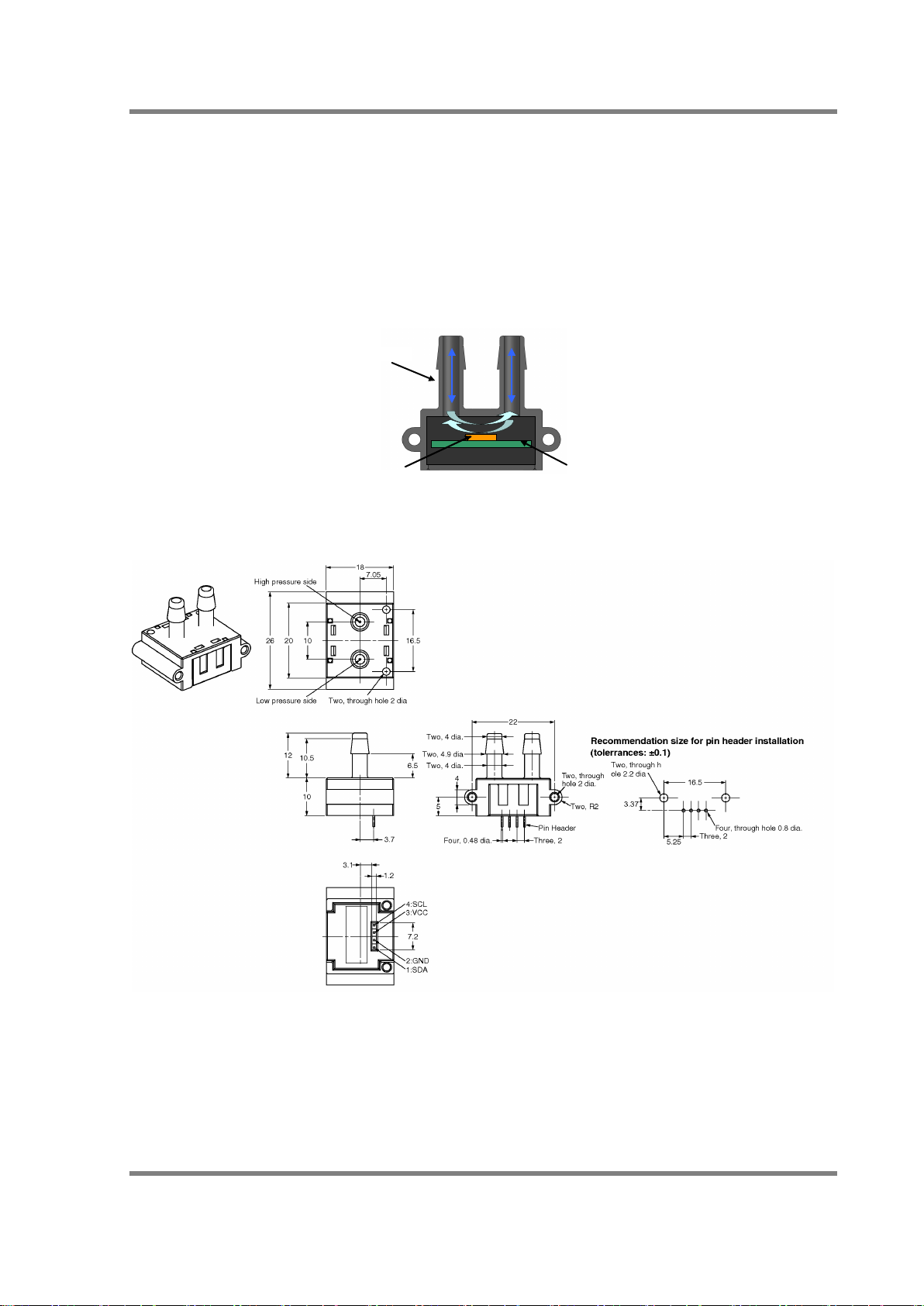
Fig.1 shows the internal cross-section view of the MEMS differential pressure sensor
(D6F-PH). Air will flow from one inlet and out the other passing over the MEMS flow chip
surface. The MEMS chip is able to measure the airflow as air passes over the chip.
Fig.1 the internal cross-section view of MEMS differential pressure sensor (D6F-PH)
3. Dimensions
Fig.2 Outline dimensions of D6F-PH
D6F-PH MEMS Differential pressure Sensor User’s Manual (A288) 2
Page 4
Orange:thermal mass flow method
chip
vVout ∝
2
main
vp ∝∆
Thermal mass flow method
proportional to the square root of
the gas flow rate through the
a conventional
square of the gas flow velocity
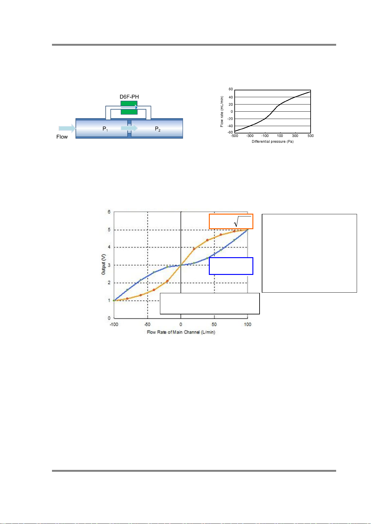
4. Principle of Pressure detection
By using a thermal mass flow sensor, Omron’s MEMS differential pressure sensor can detect
fine changes in differential pressure.
Fig. 3 Principle of differential pressure sensor (a) and relationship between flow rate
and differential pressure (b)
5. Features of Product
By using a thermal mass flow method, Omron’s MEMS differential pressure sensor is more
sensitive compared with that of a conventional differential pressure sensor in the low-pressure
range.
Blue:conventional method
Fig. 4 Comparison with conventional method and thermal mass flow method
The output of Omron’s sensor is
sensor chip surface.
Conventional method
The output of
sensor is proportional to the
through the main channel.
3 D6F-PH MEMS Differential pressure Sensor User’s Manual (A288)
Page 5

Item
Description
Min
Typ
Max
Unit
Note
Range of Differential
-50 - 50
Pa
D6F-PH0505AD3
Pressure
0 - 250
Pa
D6F-PH0025AD1
-500
-
500
Pa
D6F-PH5050AD3
Resolution
-
12 - bit
Zero point accuracy
-0.2
-
+0.2
Pa
Span accuracy
Note
-3 - +3
%R.D.
Span shift by Temperature
-0.5
-
+0.5
%R.D.
With respect to a change of
10 degC
Response Time
-
33
50
msec
12bit Resolution
Ambient Operating Temp
-20 - 80
degC
without freezing and
condensation
Ambient Storage Temp
-40 - 80
degC
without freezing and
condensation
Ambient Operating Humidity
35 - 85
%RH
without freezing and
condensation
Ambient Storage Humidity
35 - 85
%RH
without freezing and
condensation
Supply Voltage
2.3
3.3
3.6
VDC
Current Consumption
- - 6
mA
Vcc=3.3V、25degC
Frequency of SCL
- - 400
kHz
FAST Mode
Table1. Specifications of D6F-PH□□□□
(Note)
(
)
(Note)Span accuracy and zero point accuracy are the independence errors, and are not satisfied
at the same
time.
D6F-PH MEMS Differential pressure Sensor User’s Manual (A288) 4
Page 6
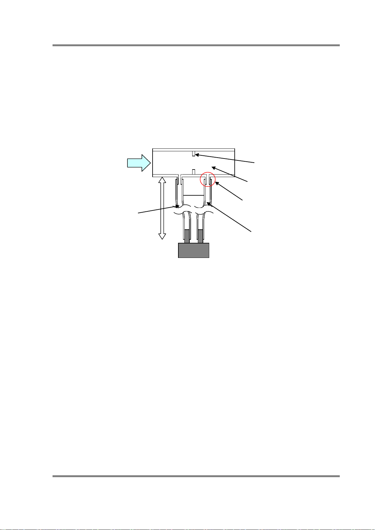
Orifice
Main Channel
Pressure Port
Flow direction
Bypass flow path
length is 800[mm] or less
High Pressure side
Lower Pressure side
6. Usage
6-1. Recommended tube connection method of D6F-PH
When connecting the D6F-PH sensor in a bypass configuration, the sensor is able to
detect fine pressure changes. This is achieved by providing an orifice in the main channel,
which generates a small pressure change before and after the orifice. The D6F-PH will be
connected to the bypass flow path from the pressure port which is provided before and after
the orifice.
of main channel
Fig. 5 Recommended tube connection method of D6F-PH
Here, the inner diameter of the bypass tube which is connected to the D6F-PH is 4[mm]
and its length is 800[mm] or less.
5 D6F-PH MEMS Differential pressure Sensor User’s Manual (A288)
Page 7
Sensor
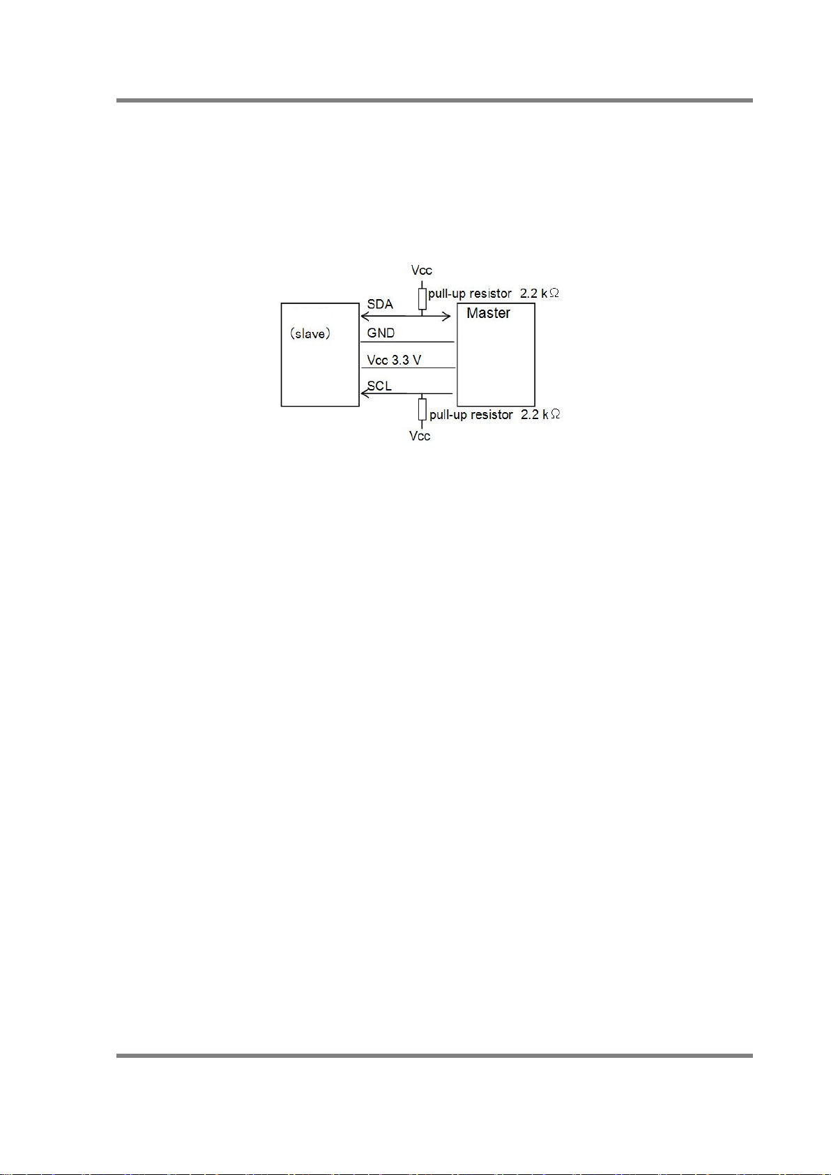
6-2. Electrical connection method of D6F-PH
For the I2C output, the D6F-PH will require a pull-up resistor to each clock line(SCL) and
data line (SDA). A pull-up resistor of 2.2[kΩ] (recommended value) should be implemented
between the Vcc as shown in Fig.6. In addition, please adjust the pull-up resistor’s value
depending on the transfer rate of SCL and the I2C wire length.
Fig. 6 Electrical connection method of D6F-PH
* Precautions when connecting the flow sensor
An error may occur during communications due to the effect of the noise of the customer’s environment.
In such a case, check the following points, and correct the communications error.
(1) Checking the communications speed
This product supports an SCL frequency of up to 400 kHz, however, if there is a likelihood of
occurrence of a communications error, we recommend using the SCL frequency at 100 kHz.
(2) Checking the wiring cable
If the length of the cable used to connect the customer-controlled microcontroller and an OMRON
flow sensor is long, the effect of noise may be more prominent. In such a case, OMRON
recommends using a shielded cable.
(3) Checking the pull-up resistor’s value
A pull-up resistor is necessary for I2C communications of this product. Although the recommended
resistor value is 2.2[kΩ], please select the optimum resistor value according to the length of the cable
used to connect the customer-controlled microcontroller and the OMRON flow sensor. A
communications error is judged unless an ACK is returned from the sensor side. The ACK response
time is equal to one clock cycle of SCL. If an ACK response is not returned after this time has
elapsed, it results in a communications error. In such a case, turn off the device.
D6F-PH MEMS Differential pressure Sensor User’s Manual (A288) 6
Page 8

D6F-PH0025AD1
D6F-PH5050AD3
D6F-PH0025AD1-1
D6F-PH5050AD3-1
D6F-PH0025AD1-2
D6F-PH5050AD3-2
D6F-PH0025AD1-3
D6F-PH5050AD3-3
Communication
method
Slave
Address
HEX
0x6C
0x6D
0x6E
0x6F
BIN (7bit)
110_1100
110_1101
110_1110
110_1111
Communications
frequency
Signal
SCL
Serial Clock
SDA
Data Signal
Bit
Bit 7
Bit 6
Bit 5
Bit 4
Bit 3
Bit 2
Bit 1
Bit 0
R/W
Value
1 1 0 1 1 0 0
1/0
Address
Register name
Descriptions
D040h
SENS_CTRL
Sensor Control
Register
D046h
FLAGS
Flag Register
D049h
INT_CTRL
CRC Calculation
Control
D051h
COMP_DATA1_H
Compensated Flow
rate Register
D052h
COMP_DATA1_L
D061h
TMP_H
Internal Temperature
Register
D062h
TMP_L
D065h
REF_FLOW1_H
Sensor Reference
Flow Register
D066h
REF_FLOW1_L
D067h
THRESH_FLOW1_H
Sensor Threshold
Flow Register
D068h
THRESH_FLOW1_L
Digital
Signal
A/D converter
I2C
Configuration
Register
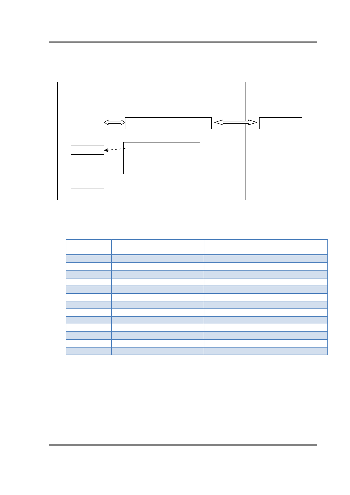
7 Specification of Communication
7-1. Outline of I2C Interface
Table2. Basic specification of I2C communication
D6F-PH0505AD3
D6F-PH0505AD3-1
Max. 400k Hz
D6F-PH0505AD3-2
I2C
D6F-PH0505AD3-3
Table 3. I2C slave address is expressed as below. (Example of 0x6C)
During Write: Set LSB of slave address to “0” to form D8h (1101_1000b).
During Read: Set LSB of slave address to “1” to form D9h (1101_1001b).
7-2. Interface Configuration Registers
The memory and registers access are controlled by writing to the interface configuration
registers.
Table4. Internal Register Map
Conditioning
Processing
7 D6F-PH MEMS Differential pressure Sensor User’s Manual (A288)
Page 9
Configuration
Address
00h
Access Address 1 (Upper byte)
Upper byte of first Access Address
01h
Access Address 2 (Lower byte)
Lower byte of first Access Address
02h
Serial Control
Write / Read Access Control
03h
Write Buffer 0
Data to be written at Address
04h
Write Buffer 1
Data to be written at Address + 1
05h
Write Buffer 2
Data to be written at Address + 2
06h
Write Buffer 3
Data to be written at Address + 3
07h
Read Buffer 0
Data read from Address
08h
Read Buffer 1
Data read from Address + 1
09h
Read Buffer 2
Data read from Address + 2
0Ah
Read Buffer 3
Data read from Address + 3
0Bh
Initialize
0Dh
Power Sequence
Hardware reset control
I2C Configuration resister
HOST
Access address
ROM / Resister
Various internal registers
In case access to internal registers are needed, the target register’s address needs to be set
to the Interface Configuration Register (address:00h and 01h).
Control
R/W Data
No. of bytes (Max. 4)
Fig. 7 Configuration overview
Table5. Interface Configuration Register Map
Function Note
Upper byte:bit[15:8] of 16bit data, Lower byte:bit[7:0] of 16bit data
D6F-PH MEMS Differential pressure Sensor User’s Manual (A288) 8
Page 10

Address
MSB
D7 D6 D5 D4 D3 D2 D1
LSB
D0
00h
A15
A14
A13
A12
A11
A10
A9
A8
01h
A7
A6
A5
A4
A3
A2
A1
A0
Address
MSB
D7 D6 D5 D4 D3 D2 D1
LSB
D0
02h
D_byte_
cnt[3]
D_byte_
cnt[2]
D_byte_
cnt[1]
D_byte_
cnt[0]
Req
R_WZ
Acc_ctl2
[1]
Acc_ctl2
[0]
7-2-1. Access Address Registers (00h – 01h)
The access address registers are used to access internal register blocks including sensor
register map, ADC register map, and internal memory. It specifies the data transfer start address
with auto increment for multiple byte data transfer.
Table6. Access Address Register
7-2-2. Serial Control Register (02h)
Table7. Serial Control Register (02h)
The serial control register contains various bits to modify the behavior of the serial access.
• Acc_ctl2 [1:0] – Access Control bits
0 0 = 16bits address (A15-A0) access ( internal ROM and registers)
0 1 = 8bits address (A7-A0) access and used to access MCU internal 256 byte dual
port RAM.
1 0 = reserved
1 1 = reserved
• R_WZ – Read or Write access select bit
0 = Write Access
1 = Read Access
• Req- Request bit
0 = the previous request is done
1 = new request. After the serial bus bridge controller finishes a request, it will clear
Req to 0. For write requests the bridge controller moves the data in write data
buffers to the location pointed by access address. For read requests the bridge
controller stores the read data into data buffer.
• D_byte_cnt3 [3:0]
Transfer data byte count. It only supports 1, 2, 3, 4 data byte transfer.
9 D6F-PH MEMS Differential pressure Sensor User’s Manual (A288)
Page 11

7-2-3. Write Buffer Registers (03h – 06h)
There are four write data buffer registers at address: 03h – 06h. To perform a write, the host
can either use a single command or perform separate writes to the following addresses.
The host can write to sensor register map in single byte transfer:
The host can burst write data start from address = 00h with following data byte,
A[15:8]、A[7:0]、18h、data[0].
Or the host can do four serial bus writes and write one data byte into serial bus register with
the following steps.
・Write A[15:8] to address = 00h of interface configuration registers.
・Write A[7:0] to address = 01h of interface configuration registers.
・Write data[0] to address = 03h of interface configuration registers.
・Write 18h to address = 18h of interface configuration registers.(1byte, new request, write)
[Note] Read Serial Control register(02h). If Req = 0 (02h[3]), controller is finished with write.
7-2-4. Read Buffer Registers (07h – 0Ah)
There are four read data buffer registers at address: 07h – 0Ah. To perform a read, the host
can either use a single streaming command or perform separate commands to the following
addresses. After the read request is done by the internal serial bus bridge controller, the Req
bit is cleared to 0 and read data is stored in rd_buf1 – rd_buf4 (address = 07h – 0Ah).
For single byte read request the host can burst write A[15:8], A[7:0], 1Ch at start address =
00h. The host needs to read the command register until the Req bit is cleared to 0, then read
“read data buffer” for read data at address = 07h.
The host can perform a single byte read by individually programming the following registers.
・Write A[15:8] to address = 00h of interface configuration registers.
・Write A[7:0] to address = 01h of interface configuration registers.
・Write 1Ch to address = 02h of interface configuration registers.(1byte, new request, read)
[Note] Read address = 02h. If Req = 0 (02h[3]), controller is finished with read data[0] from
address = 07h.
D6F-PH MEMS Differential pressure Sensor User’s Manual (A288) 10
Page 12

Address
MSB
D7 D6 D5 D4 D3 D2 D1
LSB
D0
0Dh
Hard_Rese
t
ADC_state
ADC_state
ADC_state
Pwr_seq_s
tate5
Pwr_seq_st
ate5
Pwr_seq_st
ate5
Pwr_seq_st
ate5
Bit
Name
R/W
Description
[3:0]
Pwr_seq_state5
R
Indicates the state of the power sequence.
h9(1001b): Execute
[6:4]
ADC_state
R
State in which ADC is controlled
[7]
Hard_Reset
R/W
1-> Hardware reset is performed (Automatically
0-> Hardware reset is not performed
7-2-5. Initialize (0Bh)
Initialization process after the device is turned on. Initialization must be performed to load the
trimming data of NVM.
・ Write 00h in the initialization register (0Bh)
For details, refer to Section 7-2-7. Example of I2C Access Commands.
7-2-6. Power Sequence Register (0Dh)
Table 8. Power Sequence Register (0Dh)
Table 9. Details of Power Sequence Register
h0(0000b): Idle
h2(0010b): Active
cleared after execution)
The state is h0 after the initialization process, or when the power supply is reset.
The state is h2 when 06h is written in D040.
The state is h9 during the operation.
When a hardware reset is performed, the hardware reset bit is automatically cleared to “0” after
the execution of reset, the internal register returns to the default value, and the internal trimming
value is reloaded from the non-volatile memory. This hardware reset function is similar to the
power reset function.
Notes
· When using hardware reset, set bits 0 to 6 to “0”.
11 D6F-PH MEMS Differential pressure Sensor User’s Manual (A288)
Page 13

ACK
ACK
Start address of serial
Address to be set to 00h/01h
Data to be set to 02h/03h
Start address of serial configuration
This data will be stored in serial
7-2-7. Example of I2C Access Commands
I2C Command Examples
・I2C command:I2C write
configuration registers.
START Slave Address ACK Access Address ACK Reg Address H ACK Reg Address L
S D8h (6Ch (7b)+ 0) A 00h A D0h A 40h A
of serial configuration registers.
Serial Ctrl ACK Write Data ACK STOP
18h A 06h A P
・I2C command:I2C read
registers (Read Buffer 0)
START Slave Address ACK Access Address
S D8h (6Ch (7b)+ 0) A 07h A
configuration register “07h” & “08h”
.(Read Buffer 0 / Read Buffer 1)
Re-Start Slave Address ACK Read Data H ACK Read Data L ACK STOP
RS D9h (6Ch (7b)+ 1) A xxh A xxh NA P
of serial configuration registers.
D6F-PH MEMS Differential pressure Sensor User’s Manual (A288) 12
Page 14

D7 D6 D5 D4 D3 D2 D1
D0
1]
0]
Access
MCU
MCU
MCU
Default 0 0 0 0 0 0 0 0
7-3. Description of Registers
The internal memory and registers of the sensor module can be accessed via the interface
configuration registers.
7-3-1. Sensor Control (D040h)
Table10. SENS_CTRL
Address
MSB
D040h
Write
None None
• DV_PWR[1:0] – Main Device power mode setting
0 0 = Standby – All blocks are powered down.
1 0 = MCU on – Used when only MCU is required. Basic analog and memories are
powered on and MCU clock is running.
Note :This register should not be changed during a measurement.
• MS – MCU start – Begin execution of measurement or MCU mode based on the state of
DV_PWR.
• 0 = Stop
Sequences are stopped and MCU clock is turned off.
• 1 = Start
The MCU clock is started and the MCU mode is executed.
None
MS
None None
Host &
DV_PWR[
Host &
LSB
DV_PWR[
Host &
13 D6F-PH MEMS Differential pressure Sensor User’s Manual (A288)
Page 15

D7 D6 D5 D4
D3 D2 D1
D0
D046h
OS1
HV1
SV
Access
MCU
MCU
MCU
Default 0 0 0 0 0
7-3-2. Flags (D046h)
Table11. FLAGS
Address
Write
MSB
None None
• SV – Supply Voltage (VDD) Flag
• 0 = Supply voltage is within specification.
• 1 = Supply voltage is outside of specification.
• HV1 – Heater Voltage Flag
• 0 = Heater voltage is within specification.
• 1 = Heater voltage is outside of specification.
• OS1 – Open Sensor Flag
• 0 = Sensor is connected.
• 1 = Sensor is not connected.
• HV2 and OS2 are reserved bits. In case of write access, you should set to “0”.
None
None
Host &
None
Host &
* If you want to read flag register, it is recommended to read twice in order to avoid conflict with the
MCU update.
LSB
Host &
D6F-PH MEMS Differential pressure Sensor User’s Manual (A288) 14
Page 16

D7 D6 D5 D4 D3 D2 D1
D0
D049h
CRC_EN
Access
MCU
Default 0 0 0 0 0 0 1 0
7-3-3. CRC Calculation Control ( D049h )
Table 12. INT_CTRL
ADDR
Write
• CRC_EN – CRC check calculation enable (See below for more information about the
・ CRC Overview
MSB
NONE NONE NONE NONE NONE NONE
CRC)
• 0 = CRC check calculation disable
• 1 = CRC check calculation enable
Description of the CRC calculation
The CRC is used as an error detection method in a data communication. Our flow sensor
use the CRC8 polynomial x^8 + x^5 + x^4 + 1. The following is an example of I2C access 2
byte read using CRC function.
Fig 9. Example of 2byte read with CRC
Fig.8 Example of 2byte read with CRC
Host&
LSB
NONE
15 D6F-PH MEMS Differential pressure Sensor User’s Manual (A288)
Page 17

1st Byte of data
hex
04h
02h
bin
100110001
00000010
00000100
225h
11100001
2nd Byte of data
Polynomial (x^8+ x^5+ x^4+ 1)
131h
CRC-byte checksum
Data bit sequence
0 0 0 0 0 1 0 0 0 0 0 0 0 0 1 0 0 0 0 0 0 0 0 0
1 0 0 1 1 0 0 0 1
0 0 0 1 1 0 0 0 1 1 0 0
1 0 0 1 1 0 0 0 1
0 1 0 1 1 1 1 0 1 0
1 0 0 1 1 0 0 0 1
0 0 1 0 0 1 0 1 1 0 0
1 0 0 1 1 0 0 0 1
0 0 0 0 1 1 1 0 1 0 0 0 0
1 0 0 1 1 0 0 0 1
0 1 1 1 0 0 0 0 1
1st Byte of data
2nd Byte of data
Polynomial bit sequence
・ Bit unit CRC-8 calculation method
1. The data bit sequence will be aligned in a line.
2. The polynomial bit string will be aligned under the line of the data bit sequence.
3. If the data bit above the leftmost the polynomial bit sequence is 0, the polynomial bit
sequence is shifted one bit to the right. If the data bit above the leftmost polynomial bit
sequence is 1, the data bit and the polynomial bit are calculated by XOR. Then the
polynomial bit sequence are shifted one bit to the right.
4. 1-3steps are repeated until the polynomial bit sequence reaches the right end of the data bit
sequence.
The following example shows how to calculate the CRC byte based on XOR calculation.
Fig.9 XOR operation example of CRC-8
D6F-PH MEMS Differential pressure Sensor User’s Manual (A288) 16
Page 18

D7 D6 D5 D4 D3 D2 D1
D0
COMP_DATA1_H
DATA<15:8>
COMP_DATA1_L
DATA < 7:0>
TMP_H
DATA<15:8>
TMP_L
DATA < 7:0>
7-3-4. Data Registers (D051h-D068h)
Table13. 16bit Data Register Map
Address Registers Name
D051h
D052h
D061h
D062h
MSB
LSB
For additional information, please refer to Section 8: Explanation of output data.
Description
Compensated Flow rate
Register
Internal Temperature
Register
17 D6F-PH MEMS Differential pressure Sensor User’s Manual (A288)
Page 19

8. Explanation of output data
The measured data is sent to the dedicated registers. These registers contain, respectively,
upper byte and lower byte of the sensing signals of the sensor.
For example, the compensated flow data is given by the concatenation COMP_DATA1_H &
COMP_DATA1_L in unsigned 16bit number. And the raw flow data is given by the
concatenation UCFM1_H & UCFM1_L and it is expressed as a 2’s complement of signed
16bit number.
8-1. Data alignment
Sensing data is represented as 16bit numbers. The data is split and sent in two consecutive
bytes to Flow Registers in “Big Endian” format.
“Big Endian” means that the upper byte of the number is stored in a register at the lowest
address, and the lower byte at the highest address.
8-2. Register content
・COMP_DATA1_H & COMP_DATA1_L [D051h – D052h] : Compensated Data (unsigned)
These registers contain compensated flow rate data.
○ If pressure range is ±50[Pa] or ±500[Pa]
Dp[Pa] = (Pv - 1024)/60000*RANGE – RANGE/2 (RANGE = 100 or 1000)
Where、Pv is Register content stored in the Compensated Flow Data registers [D051h
– D052h].
○ If pressure range is 0-250[Pa]
Dp[Pa] = (Pv - 1024)/60000*RANGE ( RANGE = 250 )
Where、Pv is Register content stored in the Compensated Flow Data registers [D051h
– D052h].
・TMP_H & TMP_L [D061h – D062h] : Temperature data (signed)
The values stored in these registers represent the temperature data measured by the
internal temperature of the ASIC.
The following formula can be applied to convert register data into temperature value.
℃
] = (Rv – 10214) / 37.39
Tv [
Where, Tv is Converted temperature value in the degC format, and Rv is Register
content stored in the Temperature Data register.
Note: Temperature data is for reference ONLY. Its accuracy is not specified in the
device specifications.
D6F-PH MEMS Differential pressure Sensor User’s Manual (A288) 18
Page 20

Address of Registers
Value of Registers
Converted
TMP_H
TMP_L
D061h
D062h
HEX
DEC
2Bh
8Dh
2B8Dh
11149
25.0 degC
2Eh
FFh
2EFFh
12031
48.6 degC
26h
BBh
26BBh
9915
-8.0 degC
8-3. Example of Sensing data
The below tables provide a few basic examples of the data that is read in Flow Sensor
Registers when the device is subject to given flow and temperature. The values listed in the
tables are given under the hypothesis of perfect device calibration (i.e. no offset, no gain error,
etc).
Table14. Temperature Data registers content vs. Temperature value
Temperature values
19 D6F-PH MEMS Differential pressure Sensor User’s Manual (A288)
Page 21

Item
Sign
Remarks
Response time
α
Sampling interval
β
β > α
1. Initialization
2. Execute MCU mode after desired
3. Reading the MSB and LSB of the
Enable CRC Function
*1
Hardware Reset Enable
When freezing occurs
By calling the Initialize
function of the provided
sample code, No.1 routine
By calling the Press_meas
code, No.3 routine can be
measurement, please call
Communication time
α
β
Slave
Master
4.Send
Command of data acquisition
Start of data acquisition
COMP_DATA
5.Send
Data acquisition
4.Send
Command of data acquisition
Start of data acquisition
Time
In Press_meas,
In Press_meas,
In Press_meas,
Fig.10 Flowchart of Sensor operation
8-4. Sensor Operation flow chart
configurations are set
COMP_DATA Register (D051h and D052h)
can be executed.
function of provided sample
executed.
In case of temperature
Temp_meas function.
*1 If you use CRC function, please send some command refer to Page.17.
・
α ≧ 33 ms
Fig.11 Time axis image view of the differential pressure measurement
D6F-PH MEMS Differential pressure Sensor User’s Manual (A288) 20
Page 22

ACK
18h A 06h
A
P
9. I2C Instruction for Sensor Operation
1. Initialization after power up [Must be done]
Issue this command 200 μs after turning on the power.
I2C command: The device must be unlocked then write 0x00 to the EEPROM
Control Register(0xB) to load NVM trim values, but keep the MCU
in non-reset state.
START Slave Address ACK Access Address ACK Write Data ACK STOP
S D8h (6Ch (7b)+ 0) A 0Bh A 00h A P
2. Execute MCU mode after desired configuration registers
Writing 06h to the Sensor Control Register (D040h) will execute the MCU mode outlined
in Section 6 with the configured setting for the ADC Resolution and Gain, Compensation.
Reading the Sensor control register after writing a 06h will show the MUX selection
chosen by the MCU. After running the process, MS bit will be set to “0”.
[Caution]: Do not read or write to the Device while the MCU is executing. It would be
safe to read/write only after 33ms.
I2C command: Write 06h to the Sensor Control Register (D040h) (MS=1&MCU_on)
START Slave Address ACK Access Address ACK Reg Address H ACK Reg Address L
S D8h (6Ch (7b)+ 0) A 00h A D0h A 40h A
Serial Ctrl ACK Write Data ACK STOP
21 D6F-PH MEMS Differential pressure Sensor User’s Manual (A288)
Page 23

ACK
Serial Ctrl
ACK
STOP
ACK
Re-Start
Slave Address
ACK
Read Data H
ACK
Read Data L
ACK
STOP
3. Reading the Upper and Lower byte of Compensated Flow Data Registers(D051h & D052h)
The first data after the initialization process is not the flow rate data. Disable this data.
I2C command: To read Compensated flow data register, it needs to set 2Ch (it
means 2byte read) to interface configuration register (address:2h).
START Slave Address ACK Access Address ACK Reg Address H ACK Reg Address L
S D8h (6Ch (7b)+ 0) A 00h A D0h A 51h A
I2C command: Through Read Buffer 0(address:07h) and Read Buffer 1(address:08h),
you can read the 2byte of Compensated flow data.
START Slave Address ACK Access Address
S D8h (6Ch (7b)+ 0) A 07h A
RS D9h (6Ch (7b)+ 1) A xxh A xxh NA P
2Ch A P
D6F-PH MEMS Differential pressure Sensor User’s Manual (A288) 22
Page 24

ACK
18h A 02h
A
P
4. Enable CRC Function
1. Set to "1" to bit[1] of the CRC control register.
I2C command: Write 02h to the CRC Control Register (D049h).
START Slave Address ACK Access Address ACK Reg Address H ACK Reg Address L
S D8h (6Ch (7b)+ 0) A 00h A D0h A 49h A
5. Execute Hardware Reset
1. Set to “1” to bit[7] of the Power Sequence register.
I2C command: Write 80h to the Power Sequence Register (0Dh).
START Slave Address ACK Access Address ACK Write Data ACK STOP
S D8h (6Ch (7b)+ 0) A 0Dh A 80h A P
The hardware reset after the execution, bit 7 is cleared to "0" automatically.
Serial Ctrl ACK Write Data ACK STOP
23 D6F-PH MEMS Differential pressure Sensor User’s Manual (A288)
Page 25

Please change the RANGE_MODE
define for your target Product
10. Sample Source Code
The following is a sample source code of the D6F-PH control in the case of using
STM32microcontroller. The I2C control unit will need to be adjusted to whatever microcontroller is
used.
10-1. D6F_PH_Sample.h
/*=================================================*/
/* D6F-PH Digital Flow Sensor Header File (using STM32)
* :Copyright: (C) OMRON Corporation, Microdevice H.Q.
* :Auther :
* :Revision: $Rev$
* :Id: $Id$
* :Date: $Date$
*
* All Rights Reserved
* OMRON Proprietary Right
*=================================================*/
/*=======================*/
/* for General */
/*=======================*/
#define SA_7 0x6C // for 7bit Slave Address
//#define RANGE_MODE 100 // Full Range +/-50[Pa]
#define RANGE_MODE 250 // Full Range 0-250[Pa]
//#define RANGE_MODE 1000 // Full Range +/-500[Pa]
/*=======================*/
/* for Measure Mode */
/*=======================*/
#define P 1 // Pressure mode
#define T 2 // Temperature mode
/* Function prototypes -------------------------------------------------------*/
void Initialize( void );
short Press_meas( void );
short Temp_meas( void );
/* Private Functions --------------------------------------------------------*/
int I2C_WR(unsigned char add, char *dbuf, unsigned char n);
uint8_t I2C_RD_8(unsigned char add, char *dbuf, unsigned char n);
short I2C_RD_16(unsigned char add, char *dbuf, unsigned char n);
unsigned short I2C_RD_u16(unsigned char add, char *dbuf, unsigned char n);
void I2C1_Init(void);
void I2C1_Start(void);
void I2C1_MastrSel(uint8_t address, uint8_t rw);
void I2C1_AckEn(void);
void I2C1_AckDis(void);
void I2C1_Stop(void);
void I2C1_senddata(uint8_t data);
uint8_t I2C1_rcvdata(void);
Pressure range.
D6F-PH MEMS Differential pressure Sensor User’s Manual (A288) 24
Page 26

10-2. D6F_PH_Sample.c
/*=================================================*/
/* D6F-PH Digital Flow Sensor Sample Code (using STM32)
* :Copyright: (C) OMRON Corporation, Microdevice H.Q.
* :Auther :
* :Revision: $Rev$
* :Id: $Id$
* :Date: $Date$
*
* All Rights Reserved
* OMRON Proprietary Right
*=================================================*/
#include "stm32f10x_i2c.h"
#include "D6F_PH_Sample.h"
#define I2C1_SCL_PIN GPIO_Pin_6
#define I2C1_SDA_PIN GPIO_Pin_7
#define I2C2_SCL_PIN GPIO_Pin_10
#define I2C2_SDA_PIN GPIO_Pin_11
typedef unsigned char uint8;
typedef unsigned short uint16;
typedef unsigned long uint32;
short RD_FIFO; /* 16bit data width */
unsigned short uRD_FIFO; /* 16bit data width */
uint8_t RD_REG; /* 8bit data width */
char setting_done_flag = 0;
// Dummy wait routine
void adc_wait(volatile unsigned long delay)
{
while(delay) delay--;
}
/*=================================================*/
/* Initialize Function */
/* Usage : Initialize( void ) */
/* Argument : Null */
/* Return value : T.B.D */
/*=================================================*/
void Initialize( void )
{
/* EEPROM Control <= 00h */
25 D6F-PH MEMS Differential pressure Sensor User’s Manual (A288)
Page 27

char send1[] = {0x0B, 0x00};
I2C_WR(SA_7, send1, 2);
}
/*=======================================================*/
/* Pressure measure Function */
/* Usage : Press_meas( void ) */
/* Argument : NULL */
/* Return value : Compensated Pressure value(unsigned) */
/*=======================================================*/
short Press_meas(void)
{
short rd_fifo;
short rd_flow;
unsigned long wait_time;
/* [D040] <= 06h */
char send2[] = {0x00, 0xD0, 0x40, 0x18, 0x06};
I2C_WR(SA_7, send2, 5);
wait_time = 33; /*33msec wait */
/* wait time depend on resolution mode */
adc_wait(wait_time);
/* [D051/D052] => Read Compensated Flow value */
char send3[] = {0x00, 0xD0, 0x51, 0x2C, 0x07};
uRD_FIFO = I2C_RD_u16(SA_7, send3, 5);
// Press Mode : [Pa] = (xx[count] - 1024) * Full Range [Pa]/ 60000 - Full Range [Pa] at
other
if (RANGE_MODE == 250) {
rd_flow = ((rd_fifo - 1024) * RANGE_MODE *10/ 60000); /* convert to [Pa] */
}
else {
rd_flow = ((rd_fifo - 1024) * RANGE_MODE *10/ 60000) - RANGE_MODE*10/2; /* convert
to [Pa] */
}
return rd_flow;
}
/*=======================================================*/
/* Temperature measure Function */
/* Usage : Temp_meas() */
/* Argument : NULL */
/* Return value : x10 Temperature */
/*=======================================================*/
D6F-PH MEMS Differential pressure Sensor User’s Manual (A288) 26
Page 28

short Temp_meas(void)
{
short rd_temp;
unsigned long wait_time;
/* [D040] <= 06h */
char send2[] = {0x00, 0xD0, 0x40, 0x18, 0x06};
I2C_WR(SA_7, send2, 5);
/* wait time depend on resolution mode */
wait_time = 33; /* 33msec wait */
adc_wait(wait_time);
/* [D061/D062] => Read TMP_H/TMP_L value */
char send3[] = {0x00, 0xD0, 0x61, 0x2C, 0x07};
RD_FIFO = I2C_RD_16 (SA_7, send3, 5);
rd_temp = ((RD_FIFO -10214)*1000 / 3739); // convert to degree-C(x10)
return rd_temp;
}
/* Public Basic Functions ----------------------------------------------------------*/
/*=================================================*/
/* I2C Write command */
/* Usage : I2C1_WR() */
/* Argument : 7bit Slave Address(char) */
/*
/* Return value : 8bit Read result */
/*=================================================*/
int I2C_WR(unsigned char add, char *dbuf, unsigned char n) {
int i = 0;
I2C1_Start(); /* Start condition */
I2C1_MastrSel(add, 0); /* Slave Address */
while (n--) {
I2C1_senddata(dbuf[i]); /* Send Data */
i++;
}
I2C1_Stop(); /* Stop condition */
return 0;
}
/*=================================================*/
/* I2C Read command */
/* Usage : I2C_RD() */
/* Argument : char add (7bit Slave Address) */
/* char *dbuf (Write data) */
/* unsigned char n (Number of bytes)*/
27 D6F-PH MEMS Differential pressure Sensor User’s Manual (A288)
Page 29

/* unsigned char n (Number of bytes)*/
/* Return value : 8bit Read result */
/*=================================================*/
uint8_t I2C_RD_8 (unsigned char add, char *dbuf, unsigned char n) {
int i= 0;
char n_w;
n_w = n - 1;
/* I2C Pre-WR Access */
I2C1_Start(); /* Start condition */
I2C1_MastrSel(add, 0); /* Slave Address 7bit => 8bit */
while (n_w--) {
I2C1_senddata(dbuf[i]); /* Send Data */
i++;
}
I2C1_Stop(); /* Stop condition */
/* I2C RD Access */
I2C1_Start(); /* Start condition */
I2C1_MastrSel(add, 0); /* Slave Address 7bit => 8bit */
I2C1_senddata(dbuf[n-1]); /* Word Address */
I2C1_Start(); /* Re-Start condition */
I2C1_MastrSel(add, 1); /* Slave 7bit => 8bit for RD */
I2C1_AckDis(); /* ack diable for 1 byte */
I2C1_Stop(); /* Stop condition send */
RD_REG = I2C1_rcvdata(); /* Read Data */
return RD_REG;
}
/*=================================================*/
/* I2C Read command */
/* Usage : I2C_RD_16() */
/* Argument : char add (7bit Slave Address) */
/* char *dbuf (Write data) */
/* unsigned char n (Number of bytes)*/
/* Return value : 16bit Read result */
/*=================================================*/
short I2C_RD_16 (unsigned char add, char *dbuf, unsigned char n) {
int i= 0;
char n_w;
uint8_t rd_fifo[2] = {0, 0};
n_w = n - 1;
/* I2C Pre-WR Access */
I2C1_Start(); /* Start condition */
I2C1_MastrSel(add, 0); /* Slave Address 7bit => 8bit */
while (n_w--) {
I2C1_senddata(dbuf[i]); /* Send Data */
D6F-PH MEMS Differential pressure Sensor User’s Manual (A288) 28
Page 30

i++;
}
I2C1_Stop(); /* Stop condition */
adc_wait(5); /* 5msec wait */
I2C1_Start(); /* Start condition */
I2C1_MastrSel(add, 0); /* Slave Address 7bit => 8bit */
I2C1_senddata(dbuf[n-1]); /* Word Address */
I2C1_Start(); /* Re-Start condition */
I2C1_MastrSel(add, 1); /* Slave 7bit => 8bit for RD */
I2C1_AckEn(); /* ack enable send after MSB 1 byte read */
rd_fifo[0] = I2C1_rcvdata(); /* Read Data */
I2C1_AckDis(); /* ack diable send after LSB 1 byte read */
I2C1_Stop(); /* Stop condition send */
rd_fifo[1] = I2C1_rcvdata(); /* Read Data */
RD_FIFO = ((rd_fifo[0] << 8) | rd_fifo[1]);
return RD_FIFO;
}
/*=================================================*/
/* I2C Read command */
/* Usage : I2C_RD_u16() */
/* Argument : char add (7bit Slave Address) */
/* char *dbuf (Write data) */
/* unsigned char n (Number of bytes)*/
/* Return value : 16bit Read result */
/*=================================================*/
unsigned short I2C_RD_u16 (unsigned char add, char *dbuf, unsigned char n) {
int i= 0;
char n_w;
uint8_t rd_fifo[2] = {0, 0};
n_w = n - 1;
/* I2C Pre-WR Access */
I2C1_Start(); /* Start condition */
I2C1_MastrSel(add, 0); /* Slave Address 7bit => 8bit */
while (n_w--) {
I2C1_senddata(dbuf[i]); /* Send Data */
i++;
}
I2C1_Stop(); /* Stop condition */
adc_wait(5); /* 5msec wait */
I2C1_Start(); /* Start condition */
I2C1_MastrSel(add, 0); /* Slave Address 7bit => 8bit */
I2C1_senddata(dbuf[n-1]); /* Word Address */
29 D6F-PH MEMS Differential pressure Sensor User’s Manual (A288)
Page 31

tart clock of
GPIO_InitTypeDef GPIO_InitStructure; // make instance of
event =(RW == 0)?I2C_EVENT_MASTER_TRANSMITTER_MODE_SELECTED :
I2C1_Start(); /* Re-Start condition */
I2C1_MastrSel(add, 1); /* Slave 7bit => 8bit for RD */
I2C1_AckEn(); /* ack enable send after MSB 1 byte read */
rd_fifo[0] = I2C1_rcvdata(); /* Read Data */
I2C1_AckDis(); /* ack diable send after LSB 1 byte read */
I2C1_Stop(); /* Stop condition send */
rd_fifo[1] = I2C1_rcvdata(); /* Read Data */
uRD_FIFO = ((rd_fifo[0] << 8) | rd_fifo[1]);
return uRD_FIFO;
}
void I2C1_Init(){
I2C_InitTypeDef I2C1_InitStructure;
RCC_APB1PeriphClockCmd(RCC_APB1Periph_I2C1, ENABLE); // s
I2C
I2C1_InitStructure.I2C_Mode = I2C_Mode_I2C;
I2C1_InitStructure.I2C_DutyCycle = I2C_DutyCycle_2;
I2C1_InitStructure.I2C_Ack = I2C_Ack_Enable;
I2C1_InitStructure.I2C_AcknowledgedAddress = I2C_AcknowledgedAddress_7bit;
I2C1_InitStructure.I2C_ClockSpeed = 400000;
InitStructure
RCC_APB2PeriphClockCmd(RCC_APB2Periph_GPIOB, ENABLE); // start clock of GPIO
pins
GPIO_InitStructure.GPIO_Pin =( I2C1_SCL_PIN | I2C1_SDA_PIN );
GPIO_InitStructure.GPIO_Speed = GPIO_Speed_50MHz;
GPIO_InitStructure.GPIO_Mode = GPIO_Mode_AF_OD;
GPIO_Init(GPIOB, &GPIO_InitStructure);
I2C_DeInit(I2C1);
I2C_Init(I2C1, &I2C1_InitStructure); // Initialize with above parameters
I2C_Cmd(I2C1, ENABLE);
}
void I2C1_Start(){
I2C_GenerateSTART(I2C1,ENABLE); // issue start condition
while(!I2C_CheckEvent(I2C1,I2C_EVENT_MASTER_MODE_SELECT));
}
void I2C1_MastrSel( uint8_t address, uint8_t RW){
uint8_t direct;
uint32_t event;
direct =(RW == 0)?I2C_Direction_Transmitter : I2C_Direction_Receiver;
I2C_EVENT_MASTER_RECEIVER_MODE_SELECTED;
D6F-PH MEMS Differential pressure Sensor User’s Manual (A288) 30
Page 32

transmit the received
I2C_Send7bitAddress(I2C1,(address << 1),direct ); //write to Slave
while(!I2C_CheckEvent(I2C1, event)); // wait ACK
}
void I2C1_senddata(uint8_t data){
I2C_SendData(I2C1, data); //
command
while(!I2C_CheckEvent(I2C1,I2C_EVENT_MASTER_BYTE_TRANSMITTED)); // wait ACK
}
uint8_t I2C1_rcvdata(void){
while(!I2C_CheckEvent(I2C1,I2C_EVENT_MASTER_BYTE_RECEIVED)); // wait ACK
return I2C_ReceiveData(I2C1); // receive 4th 8bit data
}
void I2C1_Stop(){
I2C_GenerateSTOP(I2C1, ENABLE); // put stop condition
}
void I2C1_AckEn(){
I2C_AcknowledgeConfig(I2C1, ENABLE); // ack enable
}
void I2C1_AckDis(){
I2C_AcknowledgeConfig(I2C1, DISABLE); // ack disable
}
31 D6F-PH MEMS Differential pressure Sensor User’s Manual (A288)
Page 33

11. WARRANTY AND LIMITED LIABILITY
Thank you for your usage of products of Omron Corporation (“Omron”). Without any special
agreements, this Terms and Conditions shall apply to all transactions regardless of who sells.
Place an order, accepting this Terms and Conditions.
1. DEFINITIONS
The following terms used herein have following meaning.
(1) Omron Products; Electronic components sold by Omron
(2) Catalogues; Any and all catalogues (including the Components Catalogue), specifications,
instructions and manuals relating to Omron Products, including electronically provided data.
(3) Conditions; Use conditions, rating, performance, operating environment, handling procedure,
precautions and/or prohibited use of Omron Products described in the Catalogues.
(4) User Application(s); Application of Omron Products by a customer, including but not limited
to embedding Omron Products into customer’s components, electronic circuit boards,
devices, equipments or systems
(5) Fitness; (a)performance, (b) no infringement of intellectual property of third party, (c)
compliance with laws and regulations and (d)conformity to various standards by Omron
Products in User Applications.
2. NOTE ABOUT DESCRIPTIONS
Please understand following as to contents of the Catalogues.
(1) Rating and performance is tested separately. Combined conditions are not warranted.
(2) Reference data is intended to be used just for reference. Omron does NOT warrant that the
Omron Product can work properly in the range of reference data.
(3) Examples are intended for reference. Omron does not warrant the Fitness in usage of the
examples.
(4) Omron may discontinue Omron Products or change specifications of them because of
improvements or other reasons.
3. NOTE ABOUT USE
Please understand followings as to your adoption and use of Omron Products
(1) Please use the product in conformance to the Conditions, including rating and performance.
(2) Please confirm the Fitness and decide whether or not Omron Products are able to be
adopted in the User Application.
(3) Omron will not warrant any items in 1.(5) (a) to (d) of User Application nor the Fitness.
(4) If you use Omron Products in the application below, please ensure followings; (i) allowance
in aspect of rating and performance, (ii) safety design which can minimize danger of the
Application when the product does not work properly and (iii) periodical maintenance of the
product and the Application.
(a) Applications requiring safety, including, without limitation, nuclear control facilities,
combustion facilities, aerospace and aviation facilities, railroad facilities, elevating
facilities, amusement facilities, medical facilities, safety devices or other applications
which has possibility to influence lives or bodies
(b) Applications requiring high reliability, including, without limitation, supplying systems of
gas, water and electric power and applications handling right, title, ownership or property,
such as payment systems
(c) Applications in a harsh condition or environment, including, without limitation, outdoor
facilities, facilities with potential of chemical contamination or electromagnetic interference,
facilities with vibration or impact and facilities on continual operation for a long period
(d) Applications under conditions or environment which are not described in this specification
(5) Omron Products shown in this catalogue are not intended to be used in automotive
applications (including two wheel vehicles). Please DO NOT use the Omron Products in the
automotive application.
(6)THE PRODUCTS CONTAINED IN THIS CATALOG ARE NOT SAFETY RATED. THEY
ARE NOT DESIGNED OR RATED FOR ENSURING SAFETY OF PERSONS, AND
D6F-PH MEMS Differential pressure Sensor User’s Manual (A288) 32
Page 34

SHOULD NOT BE RELIED UPON AS A SAFETY COMPONENT OR PROTECTIVE DEVICE
FOR SUCH PURPOSES. Please refer to separate catalogs for OMRON's safety rated
products.
4. WARRANTY
Warranty of Omron Products is subject to followings.
(1) Warranty Period; One year after your purchase
(2) Warranty; Omron will provide, free of charge, replacements of the same number of
malfunctioning products
(3) Exceptions; This warranty does not cover malfunctions caused by any of the following.
(a) Usage in the manner other than its original purpose
(b) Usage out of the Conditions
(c) Cause which could not be foreseen by the level of science and technology at the time of
shipment of the product
(d) Cause outside Omron or Omron Products, including force majeure such as disasters
5. LIMITATION ON LIABILITY
THE WARRANTY DESCRIBED IN THIS “TERMS AND CONDITIONS” IS A WHOLE AND
SOLE LIABILITY FOR OMRON PRODUCTS. THERE ARE NO OTHER WARRANTIES,
EXPRESSED OR IMPLIED. OMRON AND DISTRIBUTORS ARE NOT LIABLE FOR ANY
DAMAGES ARISEN FROM OR RELATING TO OMRON PRODUCTS.
6. PROGRAMMABLE PRODUCTS
OMRON shall not be responsible for the user's programming of a programmable product, or any
consequence thereof.
7. EXPORT CONTROLS
Buyer shall comply with all applicable laws and regulations of Japan and/or other related
countries at the time of export or provision to non-citizens of Omron Products or their technical
information.
EC200E
33 D6F-PH MEMS Differential pressure Sensor User’s Manual (A288)
Page 35

Page 36

Please check each region's Terms & Conditions by region website.
OMRON Corporation
Electronic and Mechanical Components Company
Regional Contact
Americas Europe
https://www.components.omron.com/ http://components.omron.eu/
Asia-Pacific China
https://ecb.omron.com.sg/ https://www.ecb.omron.com.cn/
Korea Japan
https://www.omron-ecb.co.kr/ https://www.omron.co.jp/ecb/
© OMRON Corporation 2018 All Rights Reserved.
In the interest of product improvement, specifications are subject to change without notice.
Cat. No. A288-E1-01
0918 (0918)(O)
 Loading...