

OMNIREL OMY440, OMY340, OMY240, OMY140 Datasheet
POWER MOSFETS IN HERMETIC ISOLATED
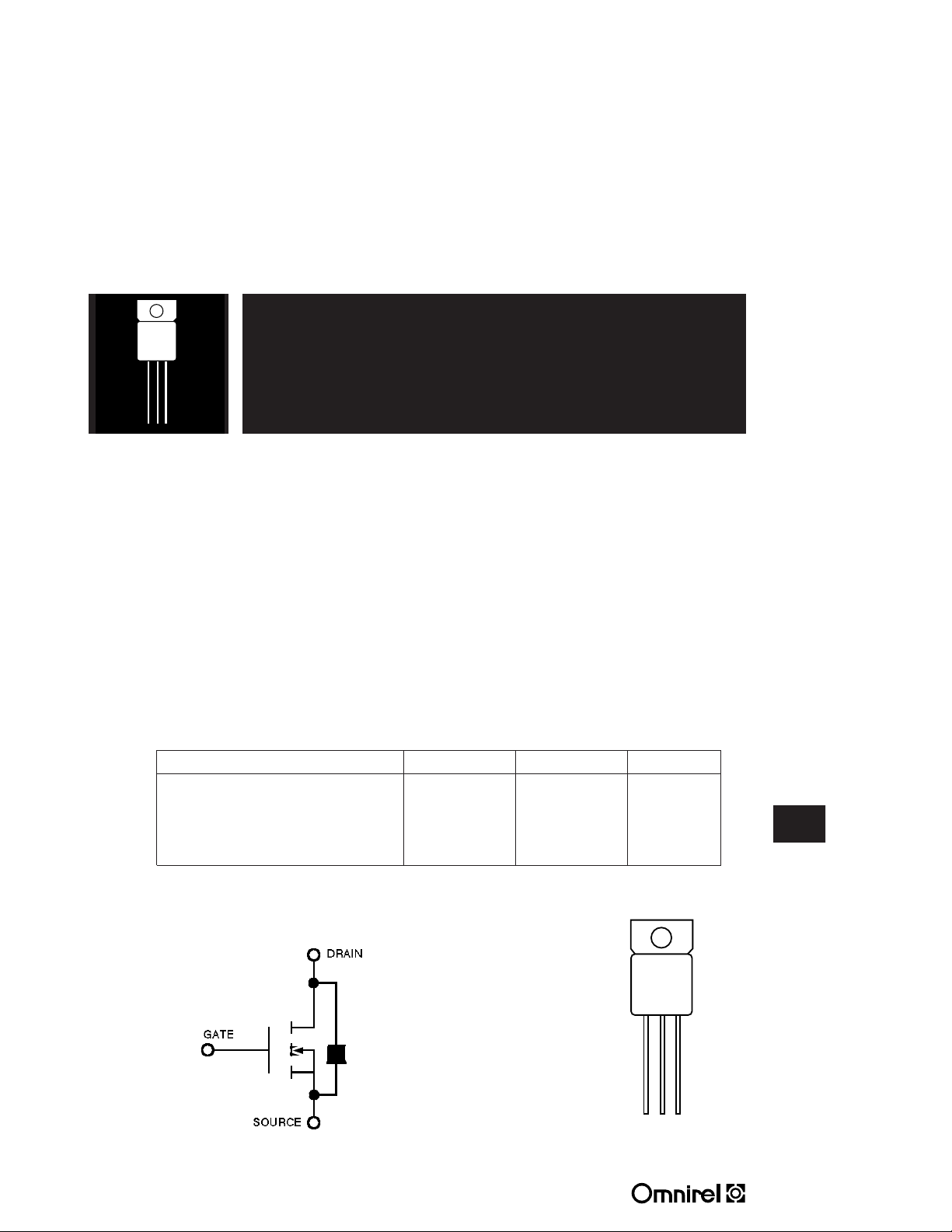
TO-257AA PACKAGE
100V Thru 500V, Up To 14 Amp, N-Channel
MOSFETs In Hermetic Metal Package
FEATURES
• Isolated Hermetic Metal Package
• Fast Switching
• Low R
• Available Screened To MIL-S-19500, TX, TXV And S Levels
• Equivalent To IRFY 140 Series
DESCRIPTION
This series of hermetically packaged products feature the latest advanced MOSFET
and packaging technology. They are ideally suited for Military requirements where
small size, high performance and high reliability are required, and in applications such
as switching power supplies, motor controls, inverters, choppers, audio amplifiers and
high energy pulse circuits.
DS(on)
OMY140
OMY240
OMY340
OMY440
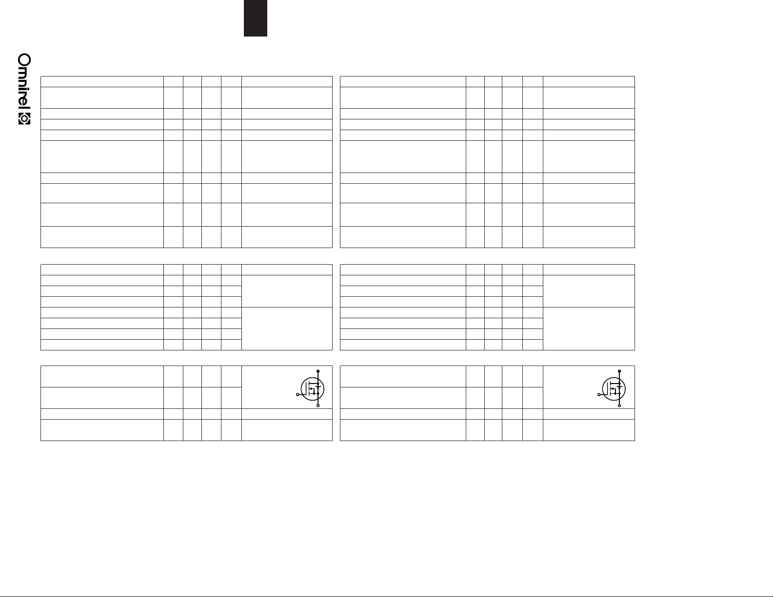
MAXIMUM RATINGS @ 25°C
PART NUMBER V
OMY140 100V .115 14A
OMY240 200V .21 14A
OMY340 400V .58 10A
OMY440 500V .88 7A
SCHEMATIC CONNECTION DIAGRAM
DS
R
DS(on)
1. GATE
2. DRAIN
3. SOURCE
I
D(MAX)
123
3.1
4 11 R2
Supersedes 1 07 R1
3.1 - 5
3.1
G
D
S
G
D
S
OMY140 - OMY440
ELECTRICAL CHARACTERISTICS: T
= 25° unless otherwise noted ELECTRICAL CHARACTERISTICS: TC= 25° unless otherwise noted
C
STATIC P/N OMY140 STATIC P/N OMY240
Parameter Min. Typ. Max. Units Test Conditions Parameter Min. Typ. Max. Units Test Conditions
BV
Drain-Source Breakdown 100 V VGS= 0, BV
DSS
Voltage I
V
Gate-Threshold Voltage 2.0 4.0 V VDS= VGS, ID= 250 mAV
GS(th)
I
Gate-Body Leakage Forward 100 nA VGS= 20 V I
GSSF
I
Gate-Body Leakage Reverse -100 nA VGS= - 20 V I
GSSR
I
Zero Gate Voltage Drain 0.1 0.25 mA VDS= Max. Rat., VGS= 0 I
DSS
Current 0.2 1.0 mA V
1
14 A VDS 2 V
3.1 - 6
I
On-State Drain Current
D(on)
V
Static Drain-Source On-State 1.40 1.73 V VGS= 10 V, ID= 15 A V
DS(on)
R
DS(on)
R
DS(on)
1
Voltage
Static Drain-Source On-State .115 VGS= 10 V, ID= 15 A R
Resistance
1
Static Drain-Source On-State .20 VGS= 10 V, ID= 15 A, R
Resistance
1
DYNAMIC DYNAMIC
g
Forward Transductance
fs
C
Input Capacitance 1275 pF VGS= 0 C
iss
C
Output Capacitance 550 pF VDS= 25 V C
oss
C
Reverse Transfer Capacitance 160 pF f = 1 MHz C
rss
T
Turn-On Delay Time 16 ns VDD= 30 V, ID@5 A T
d(on)
t
Rise Time 19 ns Rg= 5 W, VGS=10 V t
r
T
Turn-Off Delay Time 42 ns T
d(off)
t
Fall Time 24 ns t
f
1
10 S(W) VDS 2 V
= 250 mA Voltage ID= 250 mA
D
= 0.8 Max. Rat., VGS= 0, Current 0.2 1.0 mA VDS= 0.8 Max. Rat., VGS= 0,
DS
T
= 125° C TC= 125° C
C
, VGS= 10 V I
DS(on)
TC= 125 C Resistance
(W)
(MOSFET) switching times are
essentially independent of
operating temperature.
, ID= 15 A g
DS(on)
BODY-DRAIN DIODE RATINGS AND CHARACTERISTICS BODY-DRAIN DIODE RATINGS AND CHARACTERISTICS
I
Continuous Source Current - 27 A Modified MOSPOWER I
S
(Body Diode) symbol showing (Body Diode) symbol showing
I
Source Current
SM
(Body Diode) Junction rectifier. (Body Diode) Junction rectifier.
VSDDiode Forward Voltage
t
Reverse Recovery Time 200 ns TJ= 150 C,IF= IS,t
rr
1 Pulse Test: Pulse Width 300msec, Duty Cycle 2%. 1 Pulse Test: Pulse Width 300msec, Duty Cycle 2%.
1
1
- 108 A the integral P-N I
- 2.0 V TC= 25 C, IS= -24 A, VGS= 0 VSDDiode Forward Voltage
dl
/ds = 100 A/ms dlF/ds = 100 A/ms
F
Drain-Source Breakdown 200 V VGS= 0,
DSS
Gate-Threshold Voltage 2.0 4.0 V VDS= V
GS(th)
Gate-Body Leakage Forward 100 nA VGS= 20 V
GSSF
Gate-Body Leakage Reverse - 100 nA VGS= - 20 V
GSSR
Zero Gate Voltage Drain 0.1 0.25 mA VDS= Max. Rat., VGS= 0
DSS
On-State Drain Current
D(on)
Static Drain-Source On-State 1.8 2.1 V VGS= 10 V, ID= 10 A
DS(on)
DS(on)
DS(on)
fs
iss
oss
rss
d(on)
r
d(off)
f
S
SM
rr
1
Voltage
Static Drain-Source On-State 0.21 VGS= 10 V, ID= 10 A
Resistance
1
Static Drain-Source On-State 0.40 VGS= 10 V, ID= 10 A,
1
Forward Transductance
Input Capacitance 1000 pF VGS= 0
Output Capacitance 250 pF VDS= 25 V
Reverse Transfer Capacitance 100 pF f = 1 MHz
Turn-On Delay Time 17 ns VDD=75 V, ID@ 18 A
Rise Time 52 ns Rg=5 W, VGS= 10 V
Turn-Off Delay Time 36 ns
Fall Time 30 ns
Continuous Source Current - 18 A Modified MOSPOWER
Source Current
Reverse Recovery Time 350 ns TJ= 150 C,IF= IS,
1
1
1
1
14 A VDS 2 V
6.0 S(W) VDS 2 V
- 72 A the integral P-N
-1.5 V TC= 25 C, IS= -18 A, VGS= 0
, I
= 250 mA
GS
D
, VGS= 10 V
DS(on)
TC= 125 C
(W)
(MOSFET) switching times are
essentially independent of
operating temperature.
DS(on)
, ID= 10 A
 Loading...