3.5 - 99
3.5
OM7611SM
Three Terminal, Adjustable Voltage,
3.0 Amp Precision Negative Regulator
In A Hermetic Surface Mount Package
4 11 R0
SURFACE MOUNT NEGATIVE ADJUSTABLE
VOLTAGE REGULATOR
FEATURES
• Hermetic Surface Mount Package
• Adjustable Output Voltage
• Reference Voltage Set Internally to ±2%
• Built-In Thermal Overload Protection
• Short Circuit Current Limiting
• Electrically Similar To Industry Standard Type LT1033
• Product Is Available Hi-Rel Screened
DESCRIPTION
This three terminal negative regulator is supplied in a hermetically sealed surface
mount package. All protective features are designed into the circuit, including thermal
shutdown, current limiting and safe-area control. This unit features 2% initial voltage
tolerance, with 1.0% load regulation and .015% line regulation.
ABSOLUTE MAXIMUM RATINGS @ 25°C
Input Voltage...................................................................-35V
Operating Junction Temperature Range.............................-55°C to +150°C
Storage Temperature Range .........................................-65° to +150°C
Typical Power/Thermal Characteristics:
Rated Power @ 25°C........................................................15W
Thermal Resistance Junction-To-Case ...................................7.5°C/W
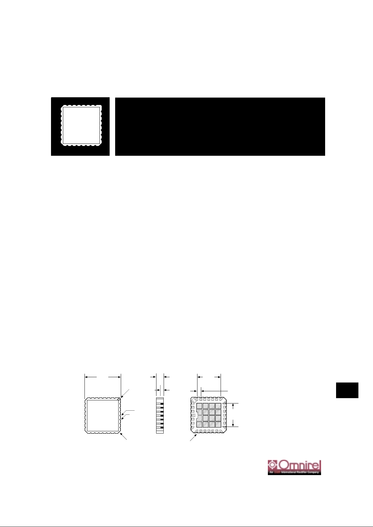
MECHANICAL OUTLINE
.450
SQ.
.300
4 PLCS.
.050
24 PLCS.
.305
SQ.
.02 x 45°
.090
MAX.
.05 X 45°
MAX. 3 PLCS.
.009 R.
28 PLCS.
.035
PIN 1
PIN 28
BOTTOMTOP SIDE
4
1
26
12
18
Pin Connection
Pin 1, 15 thru 28: OUT
Pin 2, 3, 13 and 14: ADJ
Pin 4 thru 12: IN

OM7611SM
3.5
ELECTRICAL CHARACTERISTICS -55°C ≤ T
A
≤ +125°C (unless otherwise specified)
Parameter Symbol Test Conditions Min. Max. Unit
Reference Voltage V
REF
VIN- V
OUT
= 5 V, I
OUT
= 5 mA, TA= 25° C -1.238 -1.262
V
3 V ≤ V
IN
- V
OUT
≤ 35 V • -1.215 -1.285
Line Regulation ∆V
OUT
3 V ≤ VIN- V
OUT
≤ 35 V
0.015
%/V
(Note 1) ∆V
IN
• 0.04
Load Regulation ∆V
OUT
V
OUT
≤ 5 V, TA= 25° C 50
mV
(Note 1) ∆I
OUT
10 mA ≤ I
OUT≤IMAX.
• 75
V
OUT
≥ 5.0 V 1.0
%
10 mA ≤ I
OUT≤IMAX.
• 1.5
Thermal Regulation - 30 ms pulse, T
A
= 25° C 0.02 %/W
Ripple Rejection ∆V
IN
V
OUT
= -10 V, f = 120 Hz, C
Adj
= 0
56
dB
(Note 2) ∆V
REF
• 53
V
OUT
= -10 V, f = 120 Hz, C
Adj
= 10 µF
70
dB
• 60
Adjust Pin Current I
Adj
V
DIFF
= 35 V, IL= 10 mA • 100 µA
Adjust Pin Current Change ∆I
Adj
10 mA ≤ I
OUT≤IMAX.
• 2.0
µA
3 V ≤ V
IN
- V
OUT
≤ 35 V • 5.0
Minimum Load Current I
Min
VIN- V
OUT
≤ 35 V • 10.0
mA
V
IN
- V
OUT
≤ 10 V • 5.0
Current Limit I
Lim
VIN- V
OUT
≤ 10 V
2.2 4.4
A
• 2.2
V
IN
- V
OUT
= 35 V
.35 1.88
A
• .35
Temperature Stability ∆V
OUT
-55° C ≤ TJ≤ +125° C
•
1.5 %
(Note 2) ∆T
Long Term Stability ∆V
OUT
TA= +125° C, t = 1000 hrs 1.0 %
(Note 2) ∆T
Notes:
1. Line and Load Regulation are measured at a constant junction temperature using a low duty cycle pulse technique.
Although power dissipation is internally limited, regulation is guaranteed up to the maximum power dissipation of 30 W.
Power dissipation is determined by the input/output differential voltage and the output current. Guaranteed maximum
power dissipation will not be available over the full input/output voltage range.
2. Guaranteed by design, characterization or correlation to other tested parameters.
3. The • denotes the specifications which apply over the full operating temperature range.
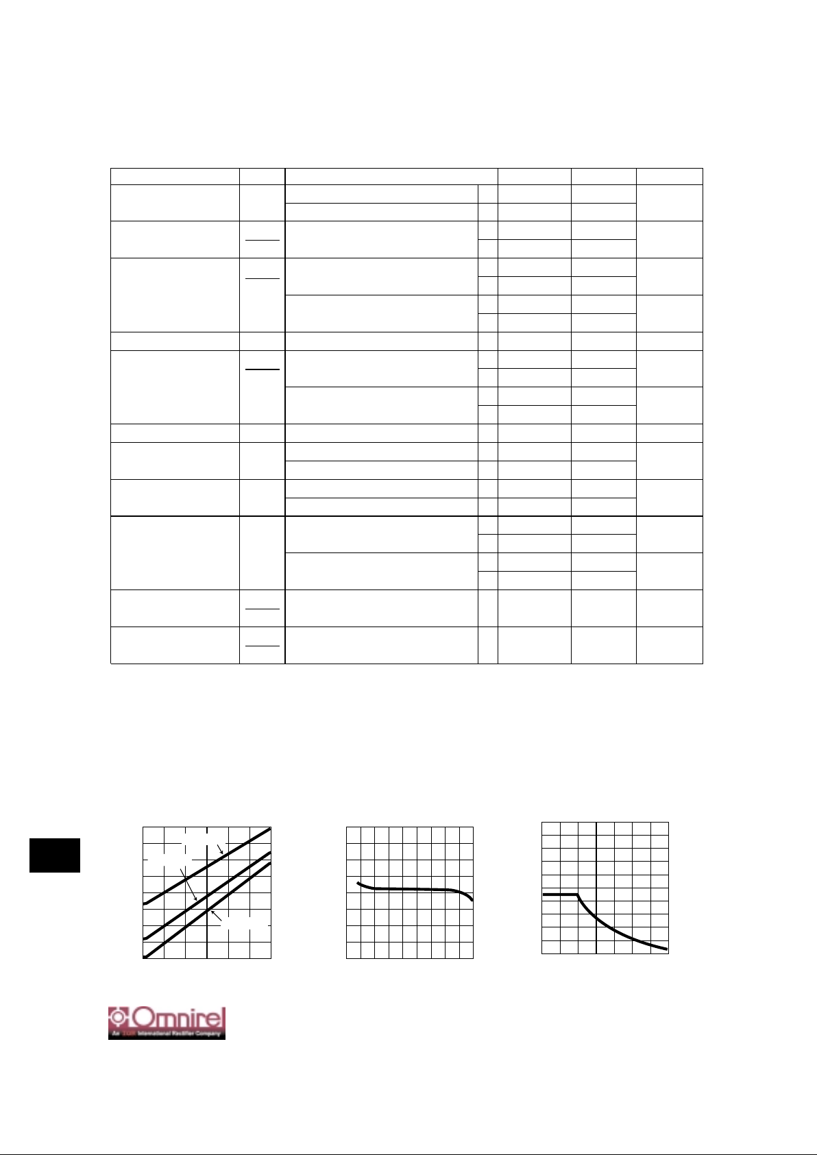
TYPICAL PERFORMANCE CURVES
Reference Voltage (V)
1.270
1.260
1.250
1.240
1.230
-75 -50 -25 0 25 50 75 100125150
Temperature (°C)
Temperature Stability
Output Current (A)
5
4
3
2
1
0
0 5 10 15 20 25 30 35
Input-Output Differential (V)
Guaranteed Minimum Output Current
Input-Output Differential (V)
2.8
2.6
2.4
2.2
2.0
1.8
1.6
1.4
1.2
0.5 1.0 1.5 2.0 2.5 3.0
Output Current (A)
Dropout Voltage
TJ = -55°C
TJ = -25°C
TJ = -150°C
 Loading...