

Page 1

2.1 - 5
2.1
4 11 R1
Supersedes 3 08 R0
Closed Loop Speed Controller For
3 Phase Brushless DC Motor
DC BRUSHLESS MOTOR CONTROLLER
FEATURES
DESCRIPTION
The OMC506 is an integrated, high density, three phase Brushless DC (BLDC)
motor, speed controller housed in a MP-3T package. The OMC506 contains the
power, driver and control electronics to adjust timing functions and speed control loop
parameters to optimize the controller for each application. The electronics contained
in the OMC506 are assembled using mixed process technologies: surface mount
components on a printed circuit board and chip & wire on an Insulated Metal
Substrate. This combination offers small size, excellent thermal characteristics and
electrically isolated heat sink.
ABSOLUTE MAXIMUM RATINGS
Motor Supply Voltage, VM………………………………………………………………32 Vdc
Peak Motor Supply Voltage, VMpk ……………………………………….….…......……48 V
Average Phase Output Current, IO ………………………………………………..…..……10 A
Pulsed Output Current (<1% Duty Cycle), I
OP
…………………………….…..…………30 A
Oscillator Input Current (Source or Sink), I
OSC
………………………………………30 mA
Reference Output Voltage V
REF(IREF
= 1.0 mA) ……………………………………..6.5 V
Digital Inputs (Fwd/Enable/Brake/SA/SB/SC) …………………………………….……..6.5 V
Reference Ouput Current, I REF (V REF=6.2 V) ………………………………………10 mA
Speed Control Input Voltage, V
SPEED
………………………………..……..…-0.3 to V REF V
Tachometer Input Voltage, V
TACH
……………………………………………..-0.3 to V REF V
Temperature Control Input Voltage, V
CNTL
… ……………………………………………..6.2 V
Regulator Output Current, (V
REG
+15V)………………………………………………100 mA
Current Sense Input Voltage, V
CS
………………………………………………...…-0.3 to 5 V
Operating Temperature Range, T
OP
…………………….…………………...…-25 to +85oC
OMC506
• 10A Average Phase Output Current
• Over Temperature Protection
• Compensation Circuitry Adjustable To Motor Parameters
• Speed Controlled by 0 To 5V Linear Input Signal
• Forward Or Reverse Direction
• Isolated, Low Profile Package
Page 2

2.1 - 6
OMC506
2.1
MP3 PACKAGE APPLICATION
ELECTRICAL CHARACTERISTICS(T
C
= 25°C unless otherwise specified)
Characteristic Symbol Test Conditions Min. Typ. Max. Unit
REFERENCE
Reference Ouput Voltage V REF I REF = 1mA 5.9 6.24 6.5 V
Reference Load Current I REF - 5 8 mA
OSCILLATOR
Oscillator Frequency F OSC 22 25 28 kHz
Sawtooth Peak Voltage V OSCpk ROSC = 4.7k, COSC = 0.01 mF - 4.1 4.5 V
Sawtooth Valley Voltage V oscva 1.2 1.5 - V
DIGITAL INPUTS
High Input Threshold Voltage V ih 3 2.2 - V
Low Input threshold Voltage V il - 1.7 0.8 V
CURRENT SENSE
Threshold Voltage V th 85 101 115 mV
Input Common ModeVolt Range V icr - 3 - V
Input Bias Current I ib - -0.9 -5 mA
VOLTAGE REGULATOR
Ouput Voltage V reg 14.0 14.5 15.0 V
Load Regulation I reg 10 mA < Io<100mA 0.1 0.3 %
THERMAL
Output Trip Voltage V OUT T > T trip’ RL =100K 13 13.31 14.79 V
Output Normal Voltage V ON T > T trip’ RL =100K - 0.13 0.4 V
Trip Temperature T trip T trip 137 145 150 C
Reset Temperature T reset 129 137 142 C
Internal Current Sense Resistor R S 9.5 10 10.5 m*
Jun to Case MOSFET Resistance R thjc - - 1.6 oC/W oC/W
A new mixed signal module fully integrates power, control functions, and drive circuitry into a
single 2" x 4" x 0.48" package. The module provides closed loop speed control of three
phase, brushless DC (BLDC) motors used in a variety of system applications . The OMC506
has been designed with flexibility in mind. Timing functions and loop parameters can be
adjusted to optimize the OMC506 to each customer’s application. In addition, the OMC506
has been designed into a MP-3T package. This package uses an insulated metal substrate,
thereby, isolating the module's electronics from chassis while providing the necessary
thermal interface for proper performance. The OMC506 offers a high efficiency, flexible,
compact, motion control system in an industry standard footprint.
Page 3
2.1 - 7
OMC506
2.1
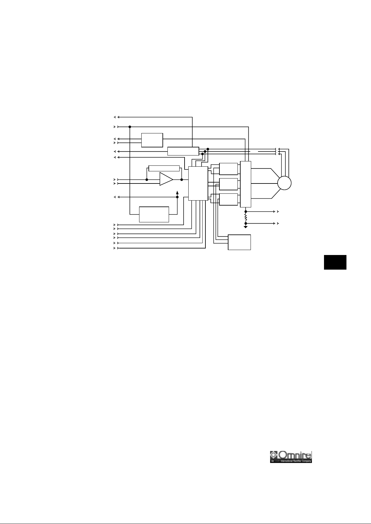
BLOCK DIAGRAM
RT/CT
V
MOTOR
CONTROL
F
OUT
6.2 V
REF
TACH IN
V
SPEED
+15 V
FWD/REV
OSC
C.S.+
C.S.-
BRAKE
ENABLE
REGULATOR
THREE
PHASE
REFRESH
R
SENSE
R
SENSE
RTN
R
SENSE
C OUT
B OUT
A OUT
MOT
POWER STAGE
SA
SC
SB
DRIVER
A
DRIVER
B
DRIVER
C
TACHOMETER
COMPENSATION
LOOP
SHAPING
+15 V
COMMUTATION
AND
CONTROL
V
OUT
OVER
TEMP
CKTRY
Controller
The OMC506 is based on the Motorola MC33035 Brushless Motor Control I.C. This controller is used in
concert with the Motorola MC33039 Closed Loop Brushless Motor Adapter I.C. to provide direct duty
cycle control of the motor speed. The OMC506 provides two quadrant speed control via an analog 0 to
5V signal applied to the V
speed
(pin 22) input. The OMC506 is selectable for 60/120 degree hall sensor
spacing. The commutation truth table for the OMC506 is shown below.
Page 4

2.1 - 8
OMC506
2.1
Table 1 - Commutation Truth Table
Closed Loop Circuits
Additional amplifiers are used in the OMC506 to provide the necessary control loop compensation for
extended bandwidth. By extending the bandwidth of the direct duty cycle control system, torque
perturbations can be accounted for while regulating the speed of the motor. This allows the module to be
used in relatively dynamic systems as well as constant torque applications. Internally, the compensation
circuitry used for control loop shaping can be tuned to optimize the OMC506 for various applications.
The OMC506 provides directional, braking, and enable interfaces from the controller I.C. (pins 32, 24,
and 25, respectively). The module also allows the user to externally set the pulse width modulation
(PWM) frequency (pin 21) as well as the pulse width from the Closed Loop Brushless Motor Adapter (pin
34). This allows a common module to be used in many applications.
Motor commutation and speed control are derived from the Hall effect sensor signals provided from the
motor. The signals are provided as inputs to the OMC506 (pins 29, 30 and 31). The amplitude of the
sensor signals must be limited, by the user, to + 6.2V to insure proper operation of the module.
Finally, the output from the Closed Loop Brushless Motor Adapter is also provided as an output of the
OMC506. This signal has a fixed amplitude and pre-set pulse width. The frequency is six times that of
the motor. This signal is integrated to produce a voltage proportional to motor speed.
Inputs Outputs
120
o
SA SB SC F/R Enable Brake AOUT BOUT COUT Fault Notes
1 0 0 1 1 0 1 - 0 1
11 0 1 1 0 - 1 0 1
01 0 1 1 0 0 1 - 1
01 1 1 1 0 0 - 1 1
00 1 1 1 0 0 - 0 1
10 1 1 1 0 1 0 - 1
10 0 0 1 0 0 - 1 1
11 0 0 1 0 - 0 1 1
01 0 0 1 0 1 0 - 1
01 1 0 1 0 1 - 0 1
00 1 0 1 0 - 1 0 1
10 1 0 1 0 0 1 - 1
1 1 1 X X 0 - - - 0 1
0 0 0 X X 0 - - - 0
1 11 X X 10 0001
0 0 X X 1 1 0 0 0 0
VVV X 1 10 0012
VV V X 0 1 0 0 0 0
VV V X 0 0 - - - 0
Notes:
1.) Invalid Sensor Inputs; X = Don’t Care
2.) V = Valid Sensor Input
Page 5

2.1 - 9
OMC506
2.1
Current Limit
The OMC506 provides outputs from the internal current sense resistor (pin 7 & 8). These outputs can be
directly wired to the C.S.+, and C.S.- (pin 28 & 27) inputs. The outputs can also be used in external
current limit circuitry. Figure 2 shows a typical connection of the OMC506’s current limit circuitry
Figure 2 - Current Limit Circuitry
Over Temperature Protection
The OMC506 has been designed with an internal over temperature protection circuit. The circuit provides
a diagnostic in the event an over temperature condition occurs in the power stage. The circuit normally
outputs a voltage level < 0.5Vdc. When the power stage reaches 140°C the V
OUT
(pin 19) will rise to
+15Vdc. The OMC506 also outputs a control function for this circuitry. A logic “0” at pin 18 will disable the
over temperature circuit and a logic “1” will force V
OUT
to go high. The over temperature circuitry has been
designed to interface with a system controller. The system controller can act on the pretense of an over
temperature and shut the OMC506 down. The system controller may opt to over ride the over temperature
flag and disable the circuit over temperature circuitry. In addition, the system controller can force the V
OUT
high as part of a built in test (BIT) feature at the system level. The over temperature circuitry will reset
when the power stage has cooled to 130°C. Finally, an internal diode can be jumpered causing the
temperature circuitry to latch on trip, requiring a power off reset.
Typical Motor Connections
Figure 3 shows a typical application of the OMC506. The user must externally connect an electrolytic
capacitor (value is dependent on the application) bypassed with a ceramic decoupling capacitor. These
capacitors should be as close to the module as feasible. In addition, it is recommended that a transient
suppressor also be added in parallel with the external capacitors to prevent high voltage transients on the
motor bus.
+
-
100
100
0.1uf 0.01uf
C.S. Amplifier
P/O MC33035
Rs
0.01
Im
P/O OMC506
28
27
8
7
To control
logic
Page 6

2.1 - 10
OMC506
2.1
Figure 3 - Typical Motor Connections
Conclusion
Omnirel’s OMC506 offers a complete motor control system, that is flexible in design, in a high density,
high power industrial module. The assembly technology makes the OMC506 an ideal candidate in
systems where package size is critical. This power module integrates all the functions necessary to
control a DC brushless motor. The design of the OMC506 is flexible enough to be customized for various
applications while still maintaining a turn-key solution to the end user. Finally, the MP310, as other
industrial packages from Omnirel, makes the user’s mechanical interface simple while optimizing the
thermal transfer from the module to the heatsink.
5 V
MOT
480µF
+
145 C TRIP
DISABLE
FORCE TRIP
DIAGNOSTIC
100K
0.01µF
0.01µF
0.1µF
80.6K634 6.65K
Power GND
Power GND
NC
Phase C
Phase C
NC
R
R
+15 V
Signal GND
Phase A
Phase A
NC
Phase B
Phase B
V
m
V
m
RT/CT
F (Tach)
Fwd/Rev
SA
SB
SC
CS+
CS-
Fault
Enable
Brake
Tach Input
V
O
sc
6.2 V
V
OUT
Control
OUT
speed
ref
sense return
V
Hall
V
MOT
sense
5 V
Page 7

OMC506
2.1
205 Crawford Street, Leominster, MA 01453 USA (508) 534-5776 FAX (508) 537-4246
Contact factory for lead bending options.
2.000
1.350
.150
(4) PLCS.
4.0003.000
.150
.500
.500
.250
.250
.600
.325
.050
(34) PLCS.
.300
.480 MAX.
.180
.020
2.450
.135
MP-3T MECHANICAL OUTLINE WITH PIN CONNECTIONS
Pin 1: Power GND
Pin 2: Power GND
Pin 3: NC
Pin 4: Phase C
Pin 5: Phase C
Pin 6: NC
Pin 7: R
sense return
Pin 8: R
sense
Pin 9: +15 V
Pin 10: Signal GND
Pin 11: Phase A
Pin 12: Phase A
Pin 13: NC
Pin 14: Phase B
Pin 15: Phase B
Pin 16: V
m
Pin 17: V
m
Pin 34: RT/CT
Pin 33: F
OUT
(Tach)
Pin 32: Fwd/Rev
Pin 31: SA
Pin 30: SB
Pin 29: SC
Pin 28: CS+
Pin 27: CSPin 26: Fault
Pin 25: Enable
Pin 24: Brake
Pin 23: Tach Input
Pin 22: V
speed
Pin 21: Osc
Pin 20: 6.2 V
REF
Pin 19: V
OUT
Pin 18: Control
 Loading...