


3.3
205 Crawford Street, Leominster, MA 01453 USA (50 8) 534-57 76 FAX (508) 537-4246
Three Terminal +5V, +12V, +15V, Low Dropout
TO-257/TO-258 Fixed Voltage Regulators
4 11 R2
Supersedes 1 07 R1
7.5A, 5A, 3A, 1.5A LOW DROPOUT
FIXED VOLTAGE POSITIVE REGULATORS
FEATURES
• +5V, +12V, and +15V Output Voltage
• Operates Down to 1V Dropout
• .015% Line Regulation / .01% Load Regulation
• Output Voltage Trimmed to ±1%
• Hermetic TO-257 and TO-258 Isolated Package
DESCRIPTION
These three terminal positive fixed voltage regulators are designed to provide 7.5A,
5A, 3A, and 1.5A with higher efficiency than conventional voltage regulators. The
devices are designed to operate to 1 Volt input to output differential and the dropout
voltage is specified as a function of load current. All devices are pin compatible with
older three terminal regulators. Supplied in the easy-to-use hermetic metal TO-257
and TO-258 JEDEC packages, these devices are ideally suited for Military
applications where small size, hermeticity and high reliability are required.
ABSOLUTE MAXIMUM RATINGS
Input Voltage . . . . . . . . . . . . . . . . . . . . . . . . . . . . . . . . . . . . . . . . . . . . . . . . . . . . 30 V
Operating Junction Temperature Range . . . . . . . . . . . . . . . . . . . . - 55°C to + 150°C
Storage Temperature . . . . . . . . . . . . . . . . . . . . . . . . . . . . . . . . . . . - 65°C to + 150°C
Output Current -OM183-5, 12, 15SC . . . . . . . . . . . . . . . . . . . . . . . . . . . . . . . . . 7.5 A
OM184-5, 12, 15SC . . . . . . . . . . . . . . . . . . . . . . . . . . . . . . . . . . . 5 A
OM185-5, 12, 15ST . . . . . . . . . . . . . . . . . . . . . . . . . . . . . . . . . . . 3 A
OM186-5, 12, 15ST . . . . . . . . . . . . . . . . . . . . . . . . . . . . . . . . . 1.5 A
Note: OM183SC and OM184SC products are packaged in the TO-258 Package (7.5A & 5A).
OM185ST and OM186ST products are packaged in the TO-257 Package (3A & 1.5A).
Part Number Designator
OM183-5SC
Omnirel Output Output Package
Current Voltage
Type
OM185-5, 12, 15ST
OM186-5, 12, 15ST
OM183-5, 12, 15SC
OM184-5, 12, 15SC
3.3 - 67
3.3
OM183-5SC - OM186-15ST
ELECTRICAL CHARACTERISTICS (T
C
= 25°C unless otherwise noted)
Parameter Conditions Min. Typ. Max. Units
Output Voltage
OM183/4/5/6 - 5 V I
OUT
= 0 mA, Tj= 25°C, VIN= 8 V 4.95 5.0 5.05 V
0 ≤ I
OUT
≤ I
FULL LOAD
, 6.5 V ≤ VIN≤ 30 V 4.90 5.0 5.10 V
OM183/4/5/6 - 12 V I
OUT
= 0 mA, Tj= 25°C, VIN= 15 V 11.88 12.0 12.12 V
0 ≤ I
OUT
≤ I
FULL LOAD
, 13.5 V ≤ VIN≤ 30 V 11.76 12.0 12.24 V
OM183/4/5/6 - 15 V I
OUT
= 0 mA, Tj= 25°C, VIN= 20 V 14.85 15.0 15.15 V
0 ≤ I
OUT
≤ I
FULL LOAD
, 17.5 V ≤ VIN≤ 30 V 14.70 15.0 15.30 V
Line Regulation
OM183/4/5/6 - 5 V I
OUT
= 0 mA, Tj= 25°C, 6.5 V ≤ VIN≤ 20 V 0.5 10 mV
1.0 10 mV
6.5 V ≤ V
IN
≤ 30 V 2.0 25 mV
OM183/4/5/6 - 12 V I
OUT
= 0 mA, Tj= 25°C, 13.5 V ≤ VIN≤ 25 V 1.0 25 mV
2.0 25 mV
13.5 V ≤ V
IN
≤ 30 V 4.0 60 mV
OM183/4/5/6 - 15 V I
OUT
= 0 mA, Tj= 25°C, 17.5 V ≤ VIN≤ 25 V 2.0 50 mV
4.0 50 mV
17.5 V ≤ V
IN
≤ 30 V 8.0 100 mV
Load Regulation
OM183/4/5/6 - 5 V V
IN
= 8 V, 0 ≤ I
OUT
≤ I
FULL LOAD
,520mV
T
j
= 25°C 10 35 mV
OM183/4/5/6 - 12 V V
IN
= 15 V, 0 ≤ I
OUT
≤ I
FULL LOAD
,1236mV
T
j
= 25°C 24 72 mV
OM183/4/5/6 - 15 V V
IN
= 20 V, 0 ≤ I
OUT
≤ I
FULL LOAD
,2040mV
T
j
= 25°C 40 100 mV
Current Limit
OM183 - 5 V V
IN
= 10 V 7.5 9.5 A
OM183 - 12 V V
IN
= 17 V 7.5 9.5 A
OM183 - 15 V V
IN
= 20 V 7.5 9.5 A
OM184 - 5 V V
IN
= 10 V 5.0 6.5 A
OM184 - 12 V V
IN
= 17 V 5.0 6.5 A
OM184 - 15 V V
IN
= 20 V 5.0 6.5 A
OM185 - 5 V V
IN
= 10 V 3.0 4.0 A
OM185 - 12 V V
IN
= 17 V 3.0 4.0 A
OM185 - 15 V V
IN
= 20 V 3.0 4.0 A
OM186 - 5 V V
IN
= 10 V 1.5 1.8 A
OM186 - 12 V V
IN
= 17 V 1.5 1.8 A
OM186 - 15 V V
IN
= 20 V 1.5 1.8 A
Dropout Voltage
OM183/4/5/6 - 5 V ∆V
OUT
= 50 mV, I
OUT
= I
FULL LOAD
6.3 6.5 V
OM183/4/5/6 - 12 V ∆V
OUT
= 120 mV, I
OUT
= I
FULL LOAD
13.3 13.5 V
OM183/4/5/6 - 15 V ∆V
OUT
= 180 mV, I
OUT
= I
FULL LOAD
17.3 17.5 V
Quiescent Current V
IN
≤ 30 V 5.0 10.0 mA
Thermal Regulation T
A
= 25°C, 30 ms pulse
OM183 - 5/12/15 V 0.002 0.01 %/W
OM184 - 5/12/15 V 0.003 0.015 %/W
OM185 - 5/12/15 V 0.004 0.02 %/W
OM186 - 5/12/15 V 0.008 0.04 %/W
Ripple Rejection f = 120 Hz, C
OUT
= 25 µF Tantalum
I
OUT
= I
FULL LOAD
OM183/4/5/6 - 5 V VIN= 8 V 63 dB
OM183/4/5/6 - 12 V V
IN
= 15 V 55 dB
OM183/4/5/6 - 15 V V
I
N
= 20 V 60 dB
Temperature Stability 0.5 %
Long Term Stability T
A
= 125°C, 1000 Hrs. 0.03 1.0 %
RMS Output Noise (% of V
OUT
)TA= 25°C, 10 Hz ≤ f ≤ 10 kHz 0.003 %
Thermal Resistance Junction-To-Case
TO-257AA 3.5 °C/W
TO-258AA 2.75 °C/W
3.3 - 68
3.3
OM183-5SC - OM186-15ST
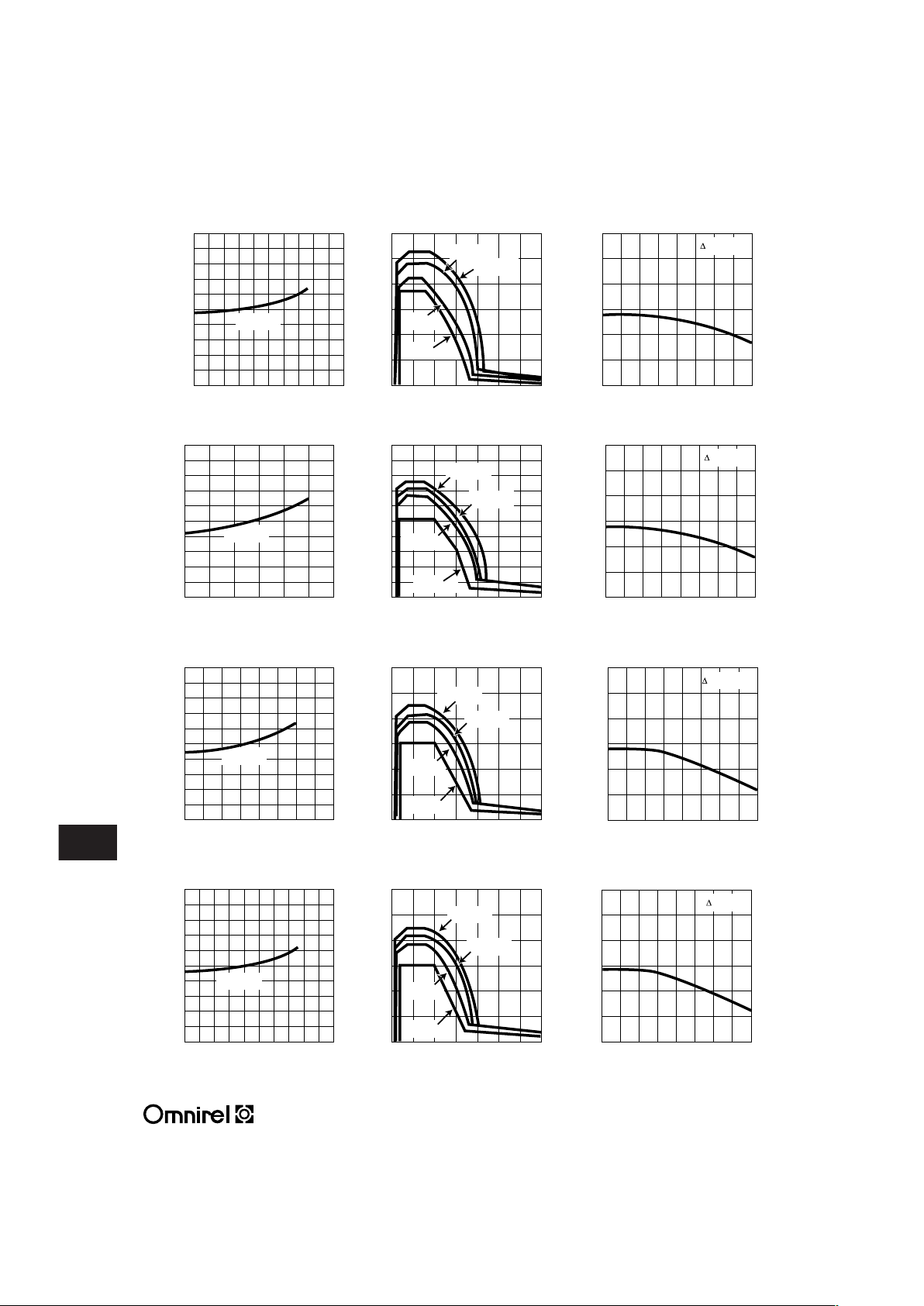
TYPICAL PERFORMANCE CHARACTERISTICS
Minimum Input/Output Differential (V)
2
1
0
012345678910
Output Current (A)
OM183SC Dropout Voltage
TJ = 25°C
Output Voltage Deviation (%)
0.10
0.05
0
-0.05
-0.10
-0.15
-0.20
-50 -25 0 25 50 75 100 125 150
Temperature (°C)
OM183SC Load Regulation
I = 7.5A
Output Voltage Deviation (%)
0.10
0.05
0
-0.05
-0.10
-0.15
-0.20
-50 -25 0 25 50 75 100 125 150
Temperature (°C)
OM184SC Load Regulation
I = 5A
Minimum Input/Output Differential (V)
2
1
0
012
Output Current (A)
OM186ST Dropout Voltage
TJ = 25°C
Output Voltage Deviation (%)
0.10
0.05
0
-0.05
-0.10
-0.15
-0.20
-50 -25 0 25 50 75 100 125 150
Temperature (°C)
OM185ST Load Regulation
I = 3A
Minimum Input/Output Differential (V)
2
1
0
0 123456
Output Current (A)
OM184SC Dropout Voltage
TJ = 25°C
Minimum Input/Output Differential (V)
2
1
0
01234
Output Current (A)
OM185ST Dropout Voltage
TJ = 25°C
Short Circuit Current (A)
12
10
8
6
4
2
0
50 101520253035
Input/Output Differential (V)
OM183SC Short Circuit Current
TJ = 150°C
TJ = -55°C
I
FULL LOAD
TJ = 25°C
Short Circuit Current (A)
10
9
8
6
6
5
4
3
2
1
0
50 10 15 20 25 30 35
Input/Output Differential (V)
OM184SC Short Circuit Current
TJ = 25°C
TJ = -55°C
I
FULL LOAD
TJ = 150°C
Short Circuit Current (A)
6
5
4
3
2
1
0
50 10 15 20 25 30 35
Input/Output Differential (V)
OM185ST Short Circuit Current
TJ = 25°C
TJ = -55°C
I
FULL LOAD
TJ = 150°C
0.10
0.05
0
-0.05
-0.10
-0.15
-0.20
-50 -25 0 25 50 75 100 125 150
Temperature (°C)
OM186ST Load Regulation
I = 3A
Output Voltage Deviation (%)
Short Circuit Current (A)
3.0
2.5
2.0
1.5
1
.5
0
50 10 15 20 25 30 35
Input/Output Differential (V)
OM186ST Short Circuit Current
TJ = 25°C
TJ = -55°C
I
FULL LOAD
TJ = 150°C

3.3 - 69
3.3
OM183-5SC - OM186-15ST
.707
.697
.750
.500
.835
.815
.695
.685
.165
.155
.200 TYP.
.550
.530
.270
.240
.045
.035
.140 TYP.
.092 MAX.
.065
.055
.005
MECHANICAL OUTLINE
PIN CONNECTION
Pin 1 - Ground
Pin 2 - V
OUT
Pin 3 - V
IN
123
PIN CONNECTION
12 3
MECHANICAL SPECIFICATIONS
P/N OM183SC and OM184SC JEDEC TO-258AA
P/N OM185ST and OM186ST JEDEC TO-257AA
MECHANICAL OUTLINE
This family of three terminal regulators is easy to use and
has all the protection features that are expected in high
performance voltage regulators. They are short circuit
protected, have safe area protection as well as thermal
shutdown to turn off the regulator should the temperature
exceed about 165°C.
These regulators offer lower dropout voltage and more
precise reference tolerance. Further, the reference stability
with temperature is improved over older types of regulators.
The only circuit difference between using this family and
older regulators is that they require an output capacitor
for stability.
Overload Recovery
When power is first turned on, as the input voltage rises,
the output follows the input, allowing the regulator to start
up into very heavy loads. During the start-up, as the input
voltage is rising, the input-to-output voltage differential
remains small, allowing the regulator to supply large output
currents. With high input voltage, a problem can occur
wherein removal of an output short will not allow the output
voltage to recover. Older regulators, such as the 7800
series, also exhibited this phenomenon, so it is not unique
to the OM183-5.
The problem occurs with a heavy output load when the
input voltage is high and the output voltage is low, such as
immediately after a removal of a short. The load line for
such a load may intersect the output current curve at two
points. If this happens, there are two stable output
operating points for the regulator. With this double
intersection, the power supply may need to be cycled down
to zero and brought up again to make the output recover.
Thermal Conditions
This series of regulators has internal power and thermal
limiting circuitry designed to protect the device under
overload conditions. For continuous normal load conditions
however, maximum junction temperature ratings must not
be exceeded. It is important to give careful consideration to
all sources of thermal resistance from junction to ambient.
This includes junction to case, case to heat sink interface,
and heat sink resistance itself. New thermal resistance
specifications have been developed to more accurately
reflect device temperature and ensure safe operating
temperatures. The data section for these new regulators
provides a separate thermal resistance and maximum
junction temperature for both the Control Section and the
Power Transistor. Previous regulators, with a single
junction to case thermal resistance specification, used an
average of the two values provided here and therefore
could allow excessive junction temperature under certain
conditions of ambient temperature and heat sink resistance.
To avoid this possibility, calculations should be made for
both sections to ensure that both thermal limits are met.
Junction-to-case thermal resistance is specified from the
IC junction to the bottom of the case directly below the die.
This is the lowest resistance path for heat flow. Proper
mounting is required to ensure the best possible thermal
flow from this area of the package to the heat sink.
Thermal compound at the case-to-heat-sink interface is
strongly recommended. If the case of the device must be
electrically isolated, a thermally conductive spacer can be
used, as long as its added contribution to thermal
resistance is considered. Note that the case of all devices
in this series is electrically connected to the output.
APPLICATION NOTES
.430
.410
.200
.190
.038 MAX.
.005
.120 TYP.
.537
.527
.665
.645
.420
.410
.150
.140
.750
.500
.100 TYP.
.035
.025
.045
.035
Pin 1 - Ground
Pin 2 - V
OUT
Pin 3 - V
IN
 Loading...