

Page 1

3.5 - 5
3.5
Three Terminal, Precision Adjustable
Positive Voltage Regulator In Hermetic
Style Packages (LM117HV)
4 11 R2
Supersedes 1 07 R1
1.5 AMP POSITIVE ADJUSTABLE VOLTAGE
REGULATOR APPROVED TO DESC DRAWING 7703402
FEATURES
• Similar To Industry Standard LM117HV
• Approved To DESC Standardized Military Drawing Number 7703402
• Built In Thermal Overload Protection
• Short Circuit Current Limiting
• Available In Six Package Styles
DESCRIPTION
These three terminal positive regulators are supplied in hermetically sealed
packages. All protective features are designed into the circuit, including thermal
shutdown, current-limiting, and safe-area control. With heat sinking, these devices
can deliver up to 1.5 amps of output current. The LCC-20 device is limited to .5
amps. The unit also features output voltages that can be fixed from 1.2 volts to 57
volts using external resistors.
ABSOLUTE MAXIMUM RATINGS T
c
@ 25°C
Power Dissipation
Case 2 . . . . . . . . . . . . . . . . . . . . . . . . . . . . . . . . . . . . . . . . . . . . . . . . . . . . . 1.1 W
Case-All Others. . . . . . . . . . . . . . . . . . . . . . . . . . . . . . . . . . . . . . . . . . . . . . . 20 W
Input - Output Voltage Differential . . . . . . . . . . . . . . . . . . . . . . . . . . . . . . . . . . . . 40 V
Operating Junction Temperature Range . . . . . . . . . . . . . . . . . . . . . - 55°C to + 150°C
Storage Temperature Range . . . . . . . . . . . . . . . . . . . . . . . . . . . . . . - 65°C to + 150°C
Lead Temperature (Soldering 10 seconds) . . . . . . . . . . . . . . . . . . . . . . . . . . . 300°C
Thermal Resistance, Junction to Case:
Case 2, LCC-20 . . . . . . . . . . . . . . . . . . . . . . . . . . . . . . . . . . . . . . . . . . . . . 17°C/W
Case U & M, TO-257 (Isol) and SMD-3 . . . . . . . . . . . . . . . . . . . . . . . . . . 4.2°C/W
Case T&N, TO-257 (Non-Isol) and SMD-1 . . . . . . . . . . . . . . . . . . . . . . . 3.5°C/W
Case Y, TO-3. . . . . . . . . . . . . . . . . . . . . . . . . . . . . . . . . . . . . . . . . . . . .3.0°C/W
Maximum Output Current:
Case 2 . . . . . . . . . . . . . . . . . . . . . . . . . . . . . . . . . . . . . . . . . . . . . . . . . . . . . . .5 A
Case-All Others. . . . . . . . . . . . . . . . . . . . . . . . . . . . . . . . . . . . . . . . . . . . . . . . 1.5 A
Recommended Operating Conditions:
Output Voltage Range . . . . . . . . . . . . . . . . . . . . . . . . . . . . . . . . . . . .1.2 to 37 VDC
Ambient Operating Temperature Range (TA). . . . . . . . . . . . . . . . - 55°C to + 125°C
Input Voltage Range . . . . . . . . . . . . . . . . . . . . . . . . . . . . . . . . . 4.25 to 41.25 VDC
OM1321STM
OM1321N2M
OM1321NMM
OM1321NTM
OM1321SMM
OM1321NKM
Please see mechanical
outlines herein
Page 2
3.5 - 6
3.5
OM1321NTM, OM1321STM, OM1321NKM, OM1321SMM, OM1321NMM, OM1321N2M
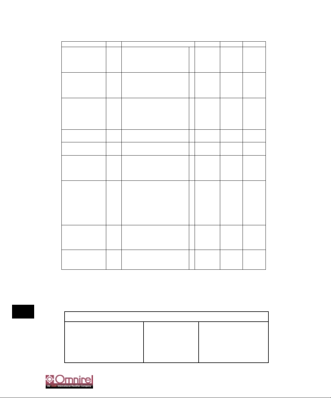
Parameter Symbol Test Conditions Min. Max. Unit
Reference Voltage V
REF
V
DIFF
= 3.0V, TA= 25°C 1.20 1.30
V
DIFF
= 3.3V • 1.20 1.30 V
V
DIFF
= 40V • 1.20 1.30
V
DIFF
= 60V • 1.20 1.30
Line Regulation R
LINE
3.0V ≤ V
DIFF
≤ 40V, V
out
= V
ref
, TA= 25°C -9 9
(Note 1) 3.3V ≤ V
DIFF
≤ 40V, V
out
= V
ref
• -23 23 mV
40V ≤ V
DIFF
≤ 60V, V
out
= V
ref
, TA= 25°C -5 5
40V ≤ V
DIFF
≤ 60V, V
out
= V
ref
• -10 10
Load Regulation R
LOADVDIFF
= 3.0V, 10mA ≤ IL≤ 1.5A, TA= 25°C -15 15
(Note 1) V
DIFF
= 3.3V, 10mA ≤ IL≤1.5A • -15 15 mV
V
DIFF
= 40V, 10mA ≤ IL≤ 300mA, TA= 25°C -15 15
V
DIFF
= 40V, 10mA ≤ IL≤ 195mA • -15 15
V
DIFF
= 60V, 10mA ≤ IL≤ 30mA • -15 15
Thermal Regulation V
RTH
Vin= 14.6V, IL= 1.5A -16 16 mV
P
d
= 20 Watts, t = 20 ms, TA= 25°C
Ripple Rejection R
N
f = 120 Hz, V
out
= V
ref
• 66 dB
(Note 2) C
Adj
= 10 µF, I
out
= 100 mA
Adjustment Pin Current I
Adj
V
DIFF
= 3.0V, TA= 25°C 100
V
DIFF
= 3.3V • 100 µA
V
DIFF
= 40V • 100
V
DIFF
= 60V • 100
Adjustment Pin ∆I
AdjVDIFF
= 3.0V, 10mA ≤ IL≤ 1.5A, TA= 25°C -5 5
Current Change V
DIFF
= 3.3V, 10mA ≤ IL≤1.5A • -5 5
V
DIFF
= 40V, 10mA ≤ IL≤ 300mA, TA= 25°C -5 5
V
DIFF
= 40V, 10mA ≤ IL≤ 195mA • -5 5 µA
3.0V ≤ V
DIFF
≤ 40V, TA= 25°C -5 5
3.3V ≤ V
DIFF
≤ 40V • -5 5
3.3V ≤ V
DIFF
≤ 60V • -5 5
Miminum Load Current I
Lmin
V
DIFF
= 3.0V, V
out
= 1.4V (forced) 5.0
V
DIFF
= 3.3V, V
out
= 1.4V (forced) • 5.0 mA
V
DIFF
= 40V, V
out
= 1.4V (forced) • 5.0
V
DIFF
= 60V, V
out
= 1.4V (forced) • 7.0
Current Limit I
CL
V
DIFF
= 5V • 1.5 3.5
(Note 2) V
DIFF
= 40V, TA= 25°C 0.3 1.5 A
V
DIFF
= 60V, TA= 25°C 0.05 0.50
Notes:
1. Load and Line Regulation are specified at a constant junction temperature. Pulse testing with low duty cycle is used.
Changes in output voltage due to heating effects must be taken into account separately.
2. If not tested, shall be guaranteed to the specified limits.
3. The • denotes the specifications which apply over the full operating temperature range.
PART NUMBER DESIGNATOR
Standard Military Drawing Number Omnirel Part Number Omnirel Package Designation
7703402M OM1321SMM SMD-3
7703402U OM1321STM TO-257 (Isolated)
7703402T OM1321NTM TO-257 (non-Isolated)
7703402Y OM1321 NKM TO-3
7703402N OM1321NMM SMD-1
77034022 OM1321N2M LCC-20
ELECTRICAL CHARACTERISTICS -55°C ≤ T
A
≤ 125°C, IL= 8mA (unless otherwise specified)
OM1321NTM, OM1321STM, OM1321NKM, OM1321SMM, OM1321NMM
Page 3
3.5 - 7
3.5
OM1321NTM, OM1321STM, OM1321NKM, OM1321SMM, OM1321NMM, OM1321N2M
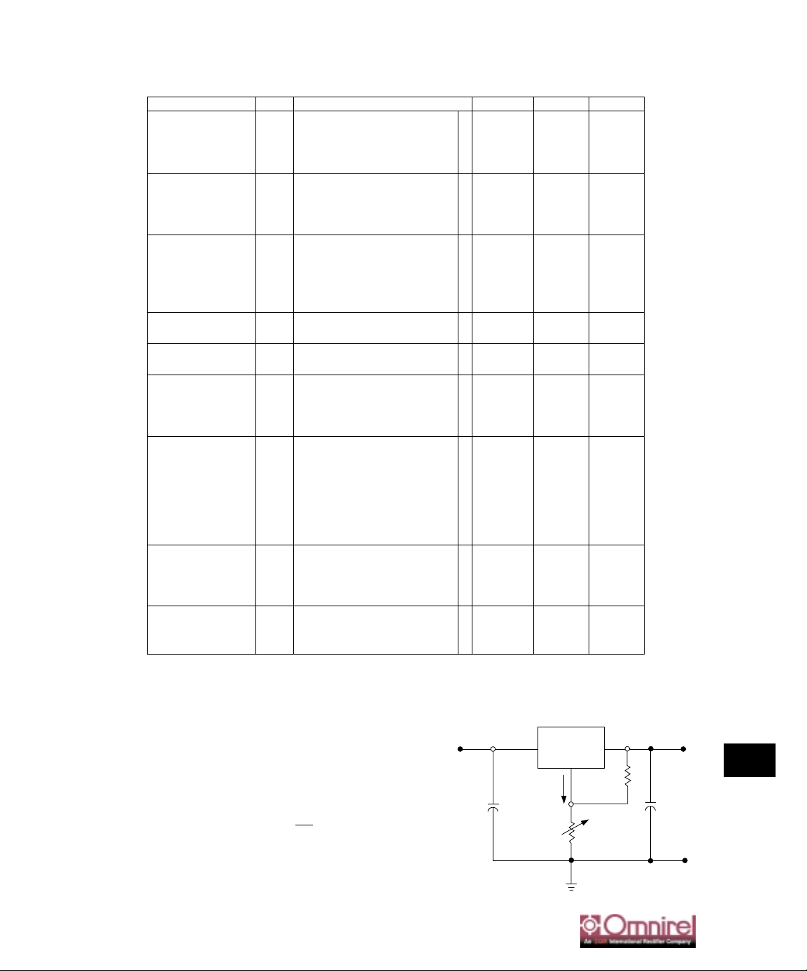
OM1321STM
V
in
Cin*
0.1 µF
V
out
Co**
1.0 µF
R
2
Adjust
I
Adj
R
1
240Ω
STANDARD APPLICATION
*Cinis required if regulator is located an
appreciable distance from power supply filter.
** C
o
is not needed for stability, however it does
improve transient response.
V
out
= 1.25 V (1 + )+ I
Ad j R2
Since I
Adj
is controlled to less than 100 µA,
the error associated with this term is negligible
in most applications.
R
2
R
1
Parameter Symbol Test Conditions Min. Max. Unit
Reference Voltage V
REF
V
DIFF
= 3.0V, TA= 25°C 1.20 1.30
V
DIFF
= 3.3V • 1.20 1.30 V
V
DIFF
= 40V • 1.20 1.30
V
DIFF
= 60V • 1.20 1.30
Line Regulation R
LINE
3.0V ≤ V
DIFF
≤ 40V, V
out
= V
ref
, TA= 25°C -9 9
(Note 1) 3.3V ≤ V
DIFF
≤ 40V, V
out
= V
ref
• -23 23 mV
40V ≤ V
DIFF
≤ 60V, V
out
= V
ref
, TA= 25°C -5 5
40V ≤ V
DIFF
≤ 60V, V
out
= V
ref
• -10 10
Load Regulation R
LOADVDIFF
= 3.0V, 10mA ≤ IL≤ 500 mA, TA= 25°C -15 15
(Note 1) V
DIFF
= 3.3V, 10mA ≤ IL≤ 500 mA • -15 15 mV
V
DIFF
= 40V, 10mA ≤ IL≤ 150 mA, TA= 25°C -15 15
V
DIFF
= 40V, 10mA ≤ IL≤ 100 mA • -15 15
V
DIFF
= 60V, 10mA ≤ IL≤ 20 mA • -15 15
Thermal Regulation V
RTH
Vin= 14.6V, IL= 300 mA -3.1 3.1 mV
P
d
= 4.0 Watts, t = 20 ms, TA= 25°C
Ripple Rejection R
N
f = 120 Hz, V
out
= V
ref
• 66 dB
(Note 2) C
Adj
= 10 µF, I
out
= 100 mA
Adjustment Pin Current I
Adj
V
DIFF
= 3.0V, TA= 25°C 100
V
DIFF
= 3.3V • 100 µA
V
DIFF
= 40V • 100
V
DIFF
= 60V • 100
Adjustment Pin ∆I
AdjVDIFF
= 3.0V, 10mA ≤ IL≤ 500 mA, TA= 25°C -5 5
Current Change V
DIFF
= 3.3V, 10mA ≤ IL≤ 500 mA • -5 5
V
DIFF
= 40V, 10mA ≤ IL≤ 150 mA, TA= 25°C -5 5
V
DIFF
= 40V, 10mA ≤ IL≤ 100 mA • -5 5 µA
3.0V ≤ V
DIFF
≤ 40V, TA= 25°C -5 5
3.3V ≤ V
DIFF
≤ 40V • -5 5
3.3V ≤ V
DIFF
≤ 60V • -5 5
Miminum Load Current I
Lmin
V
DIFF
= 3.0V, V
out
= 1.4V (forced) 5.0
V
DIFF
= 3.3V, V
out
= 1.4V (forced) • 5.0 mA
V
DIFF
= 40V, V
out
= 1.4V (forced) • 5.0
V
DIFF
= 60V, V
out
= 1.4V (forced) • 7.0
Current Limit I
CL
V
DIFF
= 5V • 0.5 1.65
(Note 2) V
DIFF
= 40V, TA= 25°C 0.15 0.65 A
V
DIFF
= 60V, TA= 25°C 0.02 0.28
Notes: Please see previous page.
ELECTRICAL CHARACTERISTICS -55°C ≤ T
A
≤ 125°C, IL= 8mA (unless otherwise specified)
OM1321N2M
Page 4
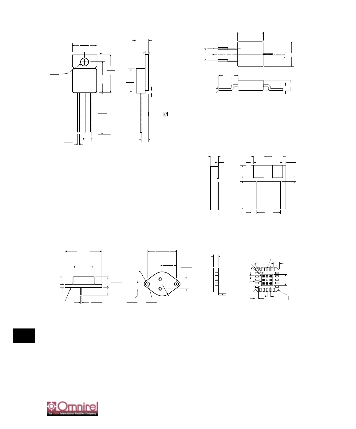
3.5
.430M
.410M
.200M
.190M
.038 MAX.M
.005M
M
.120 TYP.M
.537M
.527M
.665M
.645M
.420M
.410M
.150M
.140M
.750M
.500M
.100 TYP.M
.035M
.025M
.045M
.035M
MECHANICAL OUTLINE
.425M
.200M
M
M
M
.100M
.350 MIN.M
.080 M
M
.160M
.020M
± .020M
.035 WIDEM
FLAT 3 PLCS.M
.115M
.425M
.140
.415
.157
.015
.140
.140
.075
.075
.062
.375
.030
MIN.
.075 (±.010)
TYP.
.040.020 X45°
REF.
.040 X45°
REF (3 PL)
.010
.160
SQ. REF.
.065
.009 R.
20 PLCS.
3
1
19
18
14
4
13
9
.003
.050
TYP.
.050
(±.005)
TYP.
.085
.025 SQ.
TYP.
(±.003)
.025
TYP.
123
1
2
3
OM1321SMM
Front View
Pin 1 - Adjust
Pin 2 - Input
Pin 3 - Output
Tab - Isolated
OM1321STM OM1321NTM
Isolated Non-Isolated
Front View Front View
Pin 1 - Adjust Pin 1 - Adjust
Pin 2 - Output Pin 2 - Output
Pin 3 - Input Pin 3 - Input
Tab - Isolated Tab - Output
1
2
3
OM1321NMM
Pin 1 - Adjust
Pin 2 - Input
Pin 3 - Output
OM1321NKM
Pin 1 - Adjust
Pin 2 - Input
Case - Output
OM1321N2M
Pin 1 NC Pin 11 V
IN
Pin 2 NC Pin 12 V
OUT
Pin 3 NC Pin 13 V
OUT
Pin 4 NC Pin 14 V
OUT
(Sense)
Pin 5 NC Pin 15 NC
Pin 6 NC Pin 16 NC
Pin 7 NC Pin 17 NC
Pin 8 NC Pin 18 Adjust
Pin 9 NC Pin 19 NC
Pin 10 NC Pin 20 V
IN
For additional information please see the mechanical outline section.
OM1321NTM, OM1321STM, OM1321NKM, OM1321SMM, OM1321NMM, OM1321N2M
2
1
1.53
REF.
0.875
MAX.
0.043
0.038
2 PLCS.
0.135
MAX.
SEATING
PLANE
0.450
0.250
0.312
MIN.
0.188 R.
MAX.
0.225
0.205
1.197
1.177
0.675
0.440
0.655
0.420
0.525 R.
0.161
0.151
MAX.
 Loading...