

Page 1
MC68000"SI
NG
LE
BOARD-
COM
PUTE'R,
USER'S
MANUAL
.
01·
OMNISvTE
.
Page 2
OB68K1A
MC68000
SINGLE
BOARD
COMPUTER
USER'S
MANUAL
[]I
OMNIBYTE
The information in this document has been carefully checked and is believed to
be
entirely
reliable. However, no responsibility is assumed for inaccuracies. Furthermore, Omnibyte reserves
the right to make changes
to
any products herein to improve reliability, function, or design.
Omnibyte does not assume any liability arising out
of
the application or useofany product or cir-
cuit
described herein; neither doesitconvey any license under its patent rights nor the rights
of
others.
The technical information contained herein is provided for reference, evaluation and repair pur-
poses only and is copyrighted. It may not
be
copied or duplicated in part or in whole for any pur-
pose without the express written permission
of
Omnibyte Corporation.
VERSAbug &MACSbug are trademarksofMotorola, Inc.
MULTIBUS is a trademark
of
Intel Corporation
OB68K1
& OB68K1A are trademarks of Omnibyte Corporation
OMNIBYTE CORP •
245
West Roosevelt Road • West Chicago,
Illinois
60185 • 312/231-6880
© COPYRIGHT 1983
BY
OMNIBYTE CORPORATION
Page 3
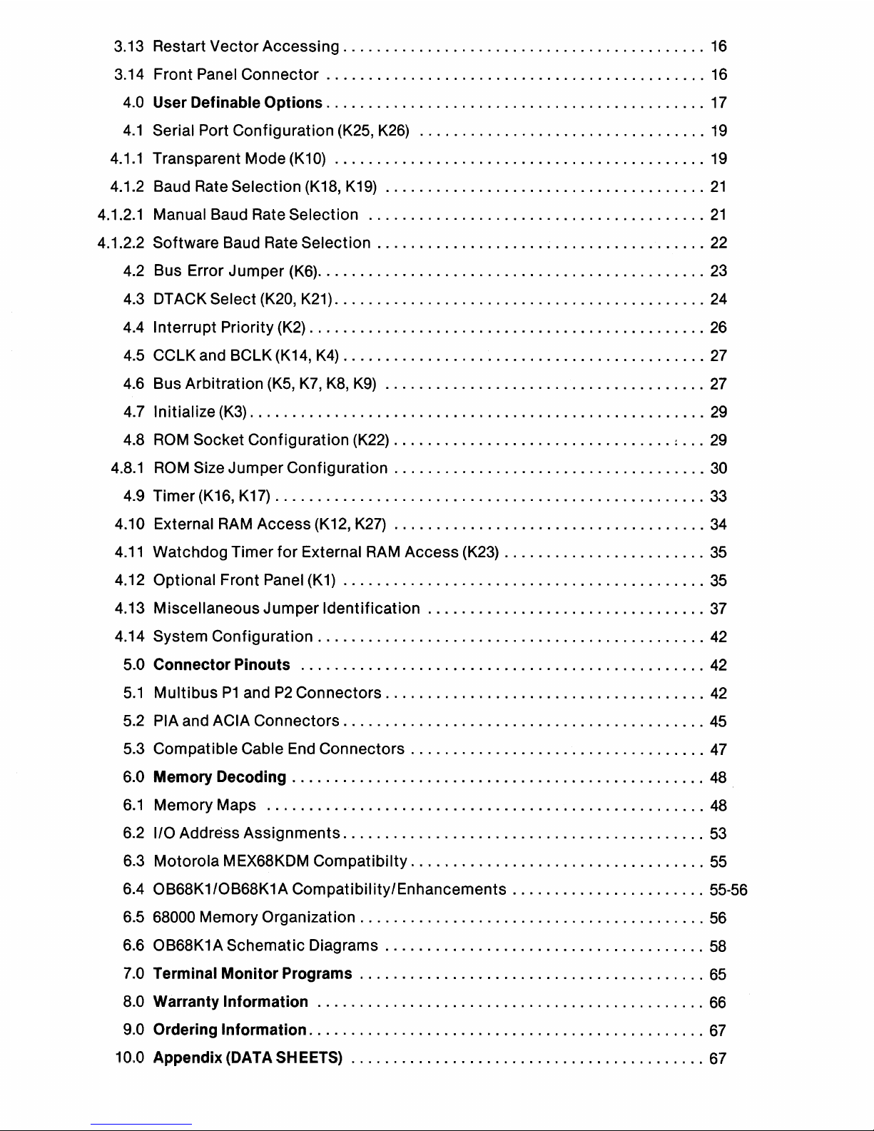
TABLE
OF
CONTENTS
Page
1.0 Introduction I Installation . . . . .. .. . . . . . . . . . . . .. . . . . . . . .. . . . . . . . . . . .
..
4
1.1
Introduction......................................................
4
1.2
Unpacking Instructions. . . .. . . . .. .. . . . . . . . . . . . . . .. . . . . . .. . . . . . . . . .
..
4
1.3
Inspection 4
1.4
Compatibility With Multibus
Products.
. .. .. . . . . . .. .. . . . . . . . .. .. .. . .
..
4
1.5
Factory Standard Configuration
5-6
2.0
Overviewofthe Computer Board. . . . . . . . . . . . . . . . . . . . . . . . . . . . . . . . . . .
..
7
2.1
SummaryofFeatures . .. .. . . . . . .. .. . . . . . . . . . . . . . . . . . . .. .. . . . . . . . .
..
7
2.2
Power Requirements. . . .. .. . . . . .. . . . . . . . . . . . . . .. . . . . . . .. . . . . . . . . .
..
7
3.0
General Description of 0
B6SK
1A 9
3.1
Serial Interface 9
3.2
Timer 9
3.3
Parallel Interface . . . . . . .. .. . . . . . . .. .. . . . . . . . .. . . . . . . . .. .. . . . . . . . .
..
9
3.4
Bus Arbitration. . . . . . . . . . . . . . . . . .... . . . . . . . . . .. . . . . . .. . . . . . . . . . . .
..
9
3.5
On-board Memory
10
3.5.1
On-board
Read
Only Memory
10
3.5.2 On-board Dynamic
RAM
10-11
3.6
Address Decoding and Memory Mapping
11
3.6.1
ROM
Address Selection
(SW-3)
12
3.6.2
RAM
Address Selection
(SW-1)
12
3.6.3
I/O
Base Address Selection
(SW-2)
12
3.6.4 External
RAM
Access Address
(SW-4)
12-13
3.6.5 Operational Considerations
13
3.6.6 Undecoded Addresses
13
3.7
Transfer Acknowledge and Bus Errors
13-14
3.8
Function Codes
14
3.9
Clocks
14
3.9.1
Processor Clock
15
3.9.2 Baud Rate Clock
15
3.9.3 Bus Clockand Constant Clock
15
3.9.4 The EClock
15
3.10 Interrupts
15
3.11
Status Indicators :
16
3.12
Single-Step Mode
16
Page 4
3.13 Restart Vector Accessing
16
3.14 Front Panel Connector
16
4.0
User Definable
Options.
. . . . . . . . . . . . . . . . . . . . . . . . . . . . . . . . . . . . . . . . . . . .
17
4.1
Serial Port Configuration (K25,
K26)
19
4.1.1
Transparent Mode
(K10)
19
4.1.2 Baud Rate Selection (K18,
K19)
21
4.1.2.1
Manual Baud Rate Selection
21
4.1.2.2 Software Baud Rate Selection
22
4.2
Bus Error Jumper
(K6)
23
4.3 DTACK Select (K20,
K21)
24
4.4 Interrupt Priority
(K2)
26
4.5
CCLK and BCLK (K14,
K4)
27
4.6
Bus Arbitration(K5,
K7, K8,
K9)
27
4.7 Initialize
(K3)
29
4.8
ROM
Socket Configuration
(K22)
:
29
4.8.1
ROM
Size JumperConfiguration
30
4.9 Timer(K16,
K17)
33
4.10 External
RAM
Access(K12,
K27)
34
4.11
Watchdog Timer
for
External
RAM
Access
(K23)
35
4.12 Optional Front Panel
(K1)
35
4.13 Miscellaneous Jumper Identification
37
4.14 System Configuration
42
5.0 Connector Pinouts
42
5.1
MultibusP1andP2Connectors
42
5.2 PIA and ACIA Connectors
45
5.3 Compatible Cable End Connectors
47
6.0 Memory Decoding
48
6.1
Memory Maps
48
6.2 I/O Address Assignments
53
6.3
Motorola MEX68KDM Compatibilty
55
6.4 OB68K1/0B68K1A Compatibility/Enhancements
55-56
6.5 68000 Memory Organization
56
6.6 OB68K1A Schematic Diagrams
58
7.0 Terminal
Monitor
Programs
65
8.0
Warranty Information
66
9.0
Ordering Information
67
10.0 Appendix(DATA SHEETS)
67
Page 5
Figure
1.0
Figure
1.1
Table
1.5
Figure
2.0
Table
4.0
Figure
4.0
Figure
4.1
Figure
4.1.1
Figure
4.1.2
Table
4.1.2.1
Table
4.3
Figure
4.3
Figure
4.4
Figure
4.6
Figure
4.7
Figure
4.8.1
Figure
4.8.2
Figure
4.8.3
Figure 4.8.4
Figure
4.9
Figure
4.10
Figure
4.12(A)
Figure
4.12(B)
Figure
4.13
Table
5.1.1
Table
5.1.2
Table
5.2.1
Table
5.2.2
Table
5.2.3
Figure
6.1.1
Figure 6.1.2
Figure 6.1.3
Figure 6.1.4
Table
6.2
Figure
6.6(A)
Figure 6.6(8)
Figure
6.6(C)
Tabl,e
6.6
LIST
OF
FIGURES AND TABLES
Photographofthe
OB68K1
A . . . . . . . . . . . . . . . . . . .. .. .. . . . . . . .
..
1
OB68K1A Parts Location
Diagram.
. . . . . . . . .. .. . . . . . . . . . . . . .
..
2
Factory JumperConfiguration 5
Block Diagram. . . . . . . . . . . . . . . . . . . . .. . . . . . . . . . . . .. .. . . . . . .
..
8
JumperOptions
17
LocationofJumperOptions
18
Serial Port JumperOptions
20
Tranparentllndep. Mode Jumper Location
21
Serial Port Baud Rate Jumpers
22
Baud Rate Selection
23
ROM
DTACKdeiays
25
ROM
DTACKdelay Jumpers
25
Interrupt Jumpers
26
Bus Arbitration JumperConfiguration
28
Reset JumperConfiguration
29
ROM
Size Jumper Configuration and Location
30
ROM
Configuration Plug Layouts
31
ROM
Socket Configuration
32
ROM
Chip Pinout Configuration
32
TimerOption Pin Identification and Location
33
External
RAM
Access Size Jumpers
34
Optional Front Panel -Connector
35
Optional Front Panel -Circuit
36
Miscellaneous Jumper Locations
37-41
IEEE-796P1Connector Pinout
43
IEEE-796P2Connector Pinout
44
PIA Connector Pinout.
45
ACIA Port 0 Connector Pinout
46
ACIA Port 1Connector Pinout
46
Memory Map (Factory Standard) 32KVersion
49
Memory Map (FactoryStandard) 128KVersion
50
Memory MapOption (MAP0)32K Version
51
Memory Map Option (MAP0)128K Version
52
Onboard I/O Address Assignments
54
OB68K1A Schematic -
CPU,
Decoding and Buffers
59
OB68K1A Schematic
-I/O
60
OB68K1
A Schematic -Memory
61
OB68K1
A Parts List
62-64
Page 6
Page 7
o
aJ
0')
co
"
.....
:I>
"'0
:I>
,,::D
_
....
C)cn
c:
....
::DO
mo
.....
:1>
.....
.....
-
o
z
c
i>
C)
::D
:I>
3:
UJ4
b'
K24
K34D
UJ2
~K231
....
R19
rn
0 0
N
I
u
5~
UJ5
C26
U60
U64
Page 8

3
Page 9
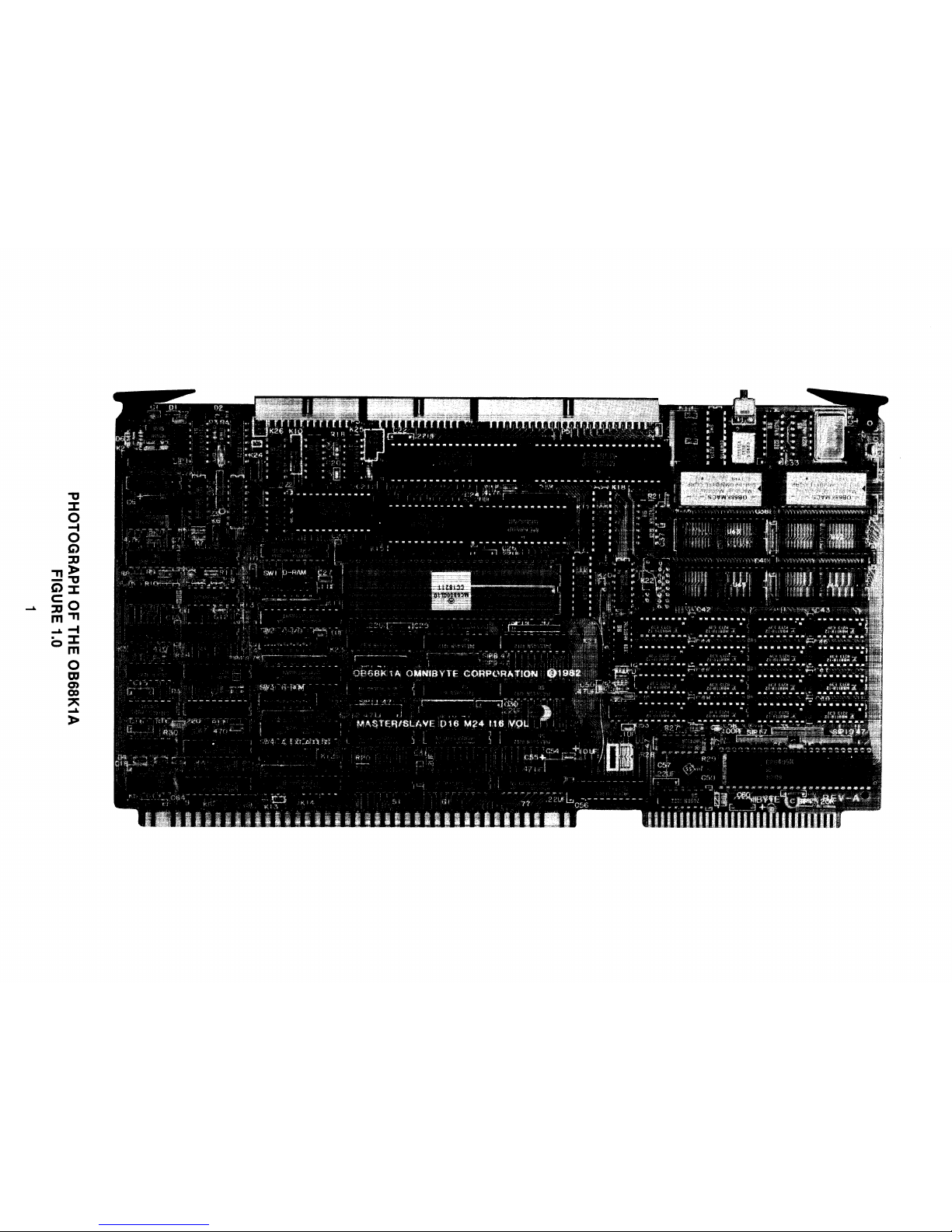
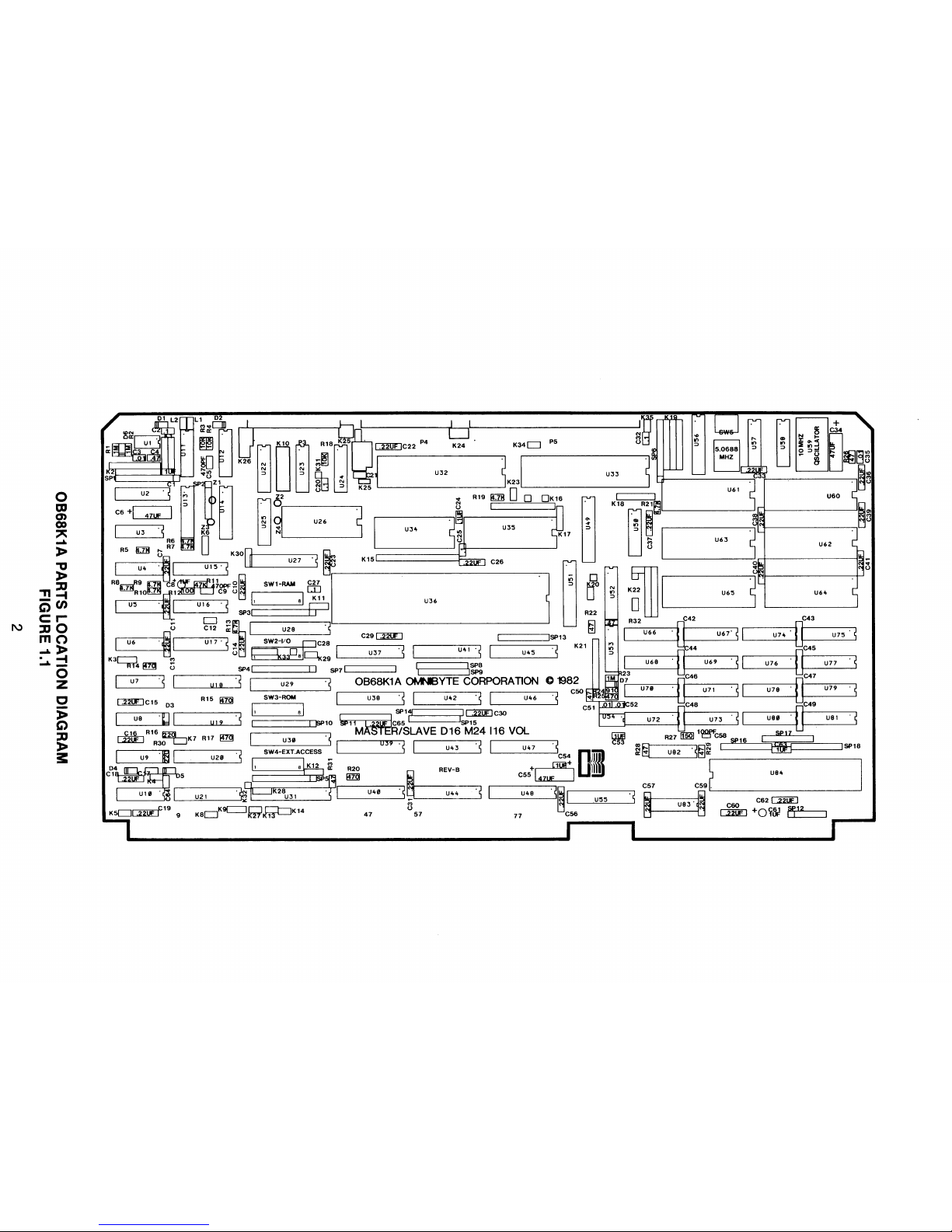
1.0 INTRODUCTION I INSTALLATION
The OMNIBYTE OB68K1A 68000 Single Board Computer has been carefully
de-
signed to
fulfill
a varietyofprocessing applications ranging from extremely small
one board dedicated instruments
to
extremely large multi-processing systems
utilizing several processor boards with shared memory and I/O. Figure
1.0
is a
photograph
of
this board and Figure
1.1
is the parts location diagram.
1.1
Introduction
This chapter provides the unpacking, inspection and configuration instructions
for the OB68K1A Single Board Computer.
1.2 Unpacking Instructions
IF THE SHIPPING CARTON
IS
DAMAGED
UPON
RECEIPT,
REQUEST THAT CARRIER'S AGENT
BE
PRESENT WHILE
THE ITEMS
ARE
BEING UNPACKED AND INSPECTED.
Unpack the OB68K1A Single Board Computer from its shipping carton. Save the
packing material for storing and reshipping the items in case this becomes
necessary.
1.3 Inspection
The OB68K1A Single Board Computer should
be
inspected upon receipt for
broken, damaged, or missing parts, and for physical damage to the printed circuit
board or connectors.
1.4 Compatibility
with
Multibus Products
The OB68K1A Single Board Computer has been carefully designed
to
meet the
most current IEEE
796
bus specifications. It is advised that you become familiar
with these specifications and how they compare with the original and current
Multibus specifications. The OB68K1A implements full address and bus arbitra-
tion for single and multi-processor systems and has been designed for com-
patibility with existing Multibus products. Omnibyte assumes no liability for
non-compatibility
of
certain products which do not meet published IEEE
796
specifications.
4
Page 10
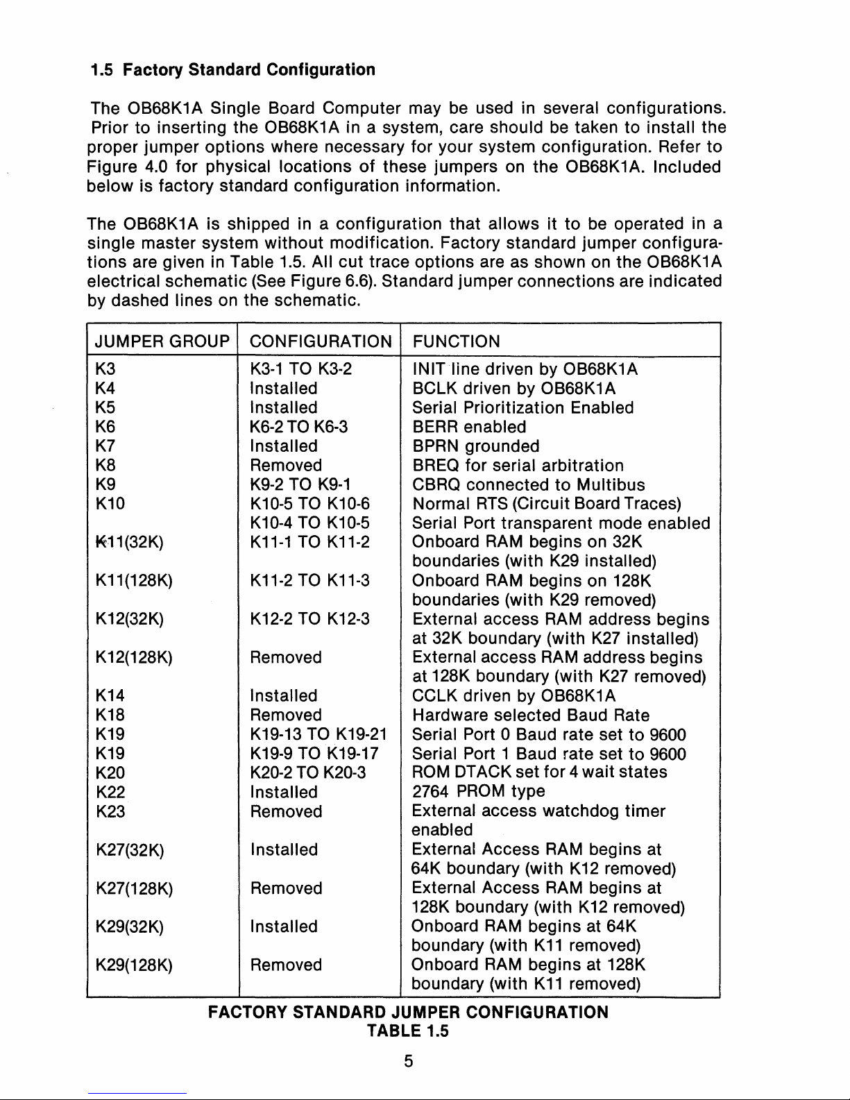
1.5 Factory Standard Configuration
The OB68K1A Single Board Computer may be used in several configurations.
Prior to inserting the OB68K1A in a system, care should be taken to install the
proper jumper
options
where necessary for your system configuration. Refer
to
Figure 4.0
for
physical locations
of
these jumpers on the OB68K1A. Included
below is factory standard configuration information.
The OB68K1A is shipped in a configuration
that
allowsitto
be operated in a
single master system
without
modification. Factory standard jumper configura-
tions
are given in Table
1.5.
All
cut
trace
options
are as shown on the OB68K1A
electrical
schematic
(See Figure
6.6).
Standard jumper connections are indicated
by dashed lines on the schematic.
JUMPER GROUP CONFIGURATION FUNCTION
K3
K3-1
TO
K3-2
INITline
driven by OB68K1A
K4
Installed
BCLK driven by OB68K1A
K5
Installed
Serial Prioritization Enabled
K6
K6-2TO
K6-3
BERR
enabled
K7
Installed BPRN grounded
K8
Removed
BREQ
for serial arbitration
K9
K9-2
TO
K9-1
CBRQ connected
to
Multibus
K10
K10-5
TO
K10-6
Normal
RTS
(Circuit Board Traces)
K10-4
TO
K10-5
Serial Port transparent mode enabled
K11(32K)
K11-1
TO
K11-2
Onboard RAM begins on 32K
boundaries (with
K29
installed)
K11(128K)
K11-2
TO
K11-3
Onboard RAM begins on 128K
boundaries (with K29 removed)
K12(32K)
K12-2
TO
K12-3
External access
RAM
address begins
at 32K boundary (with
K27
installed)
K12(128K) Removed External access RAM address begins
at 128K boundary (with
K27
removed)
K14
Installed CCLK driven by OB68K1A
K18
Removed
Hardware selected Baud Rate
K19
K19-13
TO
K19-21
Serial Port 0 Baud rate setto9600
K19
K19-9
TO
K19-17
Serial Port 1 Baud rate setto9600
K20
K20-2
TO
K20-3
ROM
DTACK set
for
4 wait states
K22
Installed
2764
PROM
type
K23
Removed
External access watchdog
timer
enabled
K27(32K)
Installed
External Access RAM begins at
64K boundary (with
K12
removed)
K27(128K) Removed
External Access RAM begins at
128K boundary (with
K12
removed)
K29(32K)
Installed
Onboard RAM begins at 64K
boundary (with
K11
removed)
K29(128K) Removed
Onboard RAM begins at 128K
boundary (with
K11
removed)
FACTORY STANDARD JUMPER CONFIGURATION
TABLE 1.5
5
Page 11
The
OB68K1
A is configured at the factory to operate in the following way;
a)
BUS
The Bus Clock (BCLK), Constant Clock (CCLK) and Reset line (INIT) are driven
off
the board. On-board power-on reset enabled and the bus error jumper
(K6)
is in-
stalled so that bus error exception processing will
be
executed,ifa bus error is
encountered.
b)
INTERRUPTS
No interrupts are connected.
c)
RAM
On-board
RAM
begins at
$000000
(HEX).
Contiguous
RAM
continues
to
$007FFF
(HEX)
in the 32K version and to $01 FFFF
(HEX)
in the 128K version.
d)
ROM
All on-board
ROM
sockets are configured for 2764-type (8Kx8) 5 volt only
EPROM
and the memory map is configured to MAP 1 (for
2764).
ROM
address begins at
$FEOOOO
(HEX)
and continues to $FEFFFF
(HEX).
The
ROM
DTACK is factory
preset for
350
ns (access time)
ROM
chips.
e)
ON-BOARD SERIAL 1/0
PORTS
On-board 1/0 begins at address $FFFEOO
(HEX).
See table
6.2
for specific device
address assignments. Serial Port 0 is configured as a modem for direct connection to a
RS232C
terminal. Serial Port 1 is configured as a terminal for direct con-
nection to a
RS232C
modem or another computer. The baud rates are set to 9600
BPS
at the factory for testing.
f)
OFF-BOARD 1/0
Off-board 1/0 begins at address $FFOOOO
(HEX)
and continues to $FFFDFF.
g)
TRANSPARENT MODE
Transparent mode is enabled.
Please note that the above is the configuration
of
the OB68K1A as shipped from
the factory and
it
does not include setting-up the board in a different configura-
tion
if
desired before power-up_ A detailed listofthe factory installed jumper con-
figurations is given in Table
1.5.
Factory standard configuration is compatible
with Omnibyte's optional
PROM
based terminal monitor routines that provide the
functionality
of
Motorola's MACSbug/VERSAbug/VMEbug/TUTOR programs.
6
Page 12
2.0 OVERVIEW OF THE COMPUTER BOARD
This
section
describes the
major
features
of
the OB68K1A. A
block
diagram
of
this
single
board
computer
is shown in Figure 2.0.
2.1
SummaryofFeatures
The OB68K1A
computer
board provides the
following
features:
a.
10MHz processor &
clock
b.
IEEE 796 (Multibus) Compatible (MASTER
D16
M24
116
VOUSLAVE M24
D16)
c. Single step
circuitry
d. Dual Ported on-board RAM (32K byteor128K byte)
e.
Zero
wait
states
for on-board RAM accesses
f.
LSI
Hardware memory refresh
circuit
g.
On-board
ROM
(up
to
192K bytes)
h.
Two asynchronous serial
ports
(RS232C)
i.
Hardware
or
software programmable baud rate generator
j. Two programmable 16-bit parallel I/O ports
k.
Three 16-bit programmable
timers
I.
16
Megabyte (24-bit)
direct
memory addressing
m.
Independantly
Switch
Selectable RAM, ROM,
EXT.
RAM ACCESS, and
I/O base addresses
n.
Multi-Master
bus
arbitration
o.
Motorola
MEX68KDM
software
compatibility
2.2 Power Requirements
The
computer
receives
its
power through the
Multibus
motherboard. Typical
power requirements are as follows:
+
5V
- ±
50/0
+ 12V - ±
5%
-12V-
± 5
%
32K VERSION 128 K VERSION
@ 3.0A @ 3.25A
@
O.05A
@ 0.05A
@
O.05A
@
O.05A
Note: Single 5 volt operation is possible
with
the OB68K1 Aifthe RS232C
ports
are
not
used.
7
Page 13
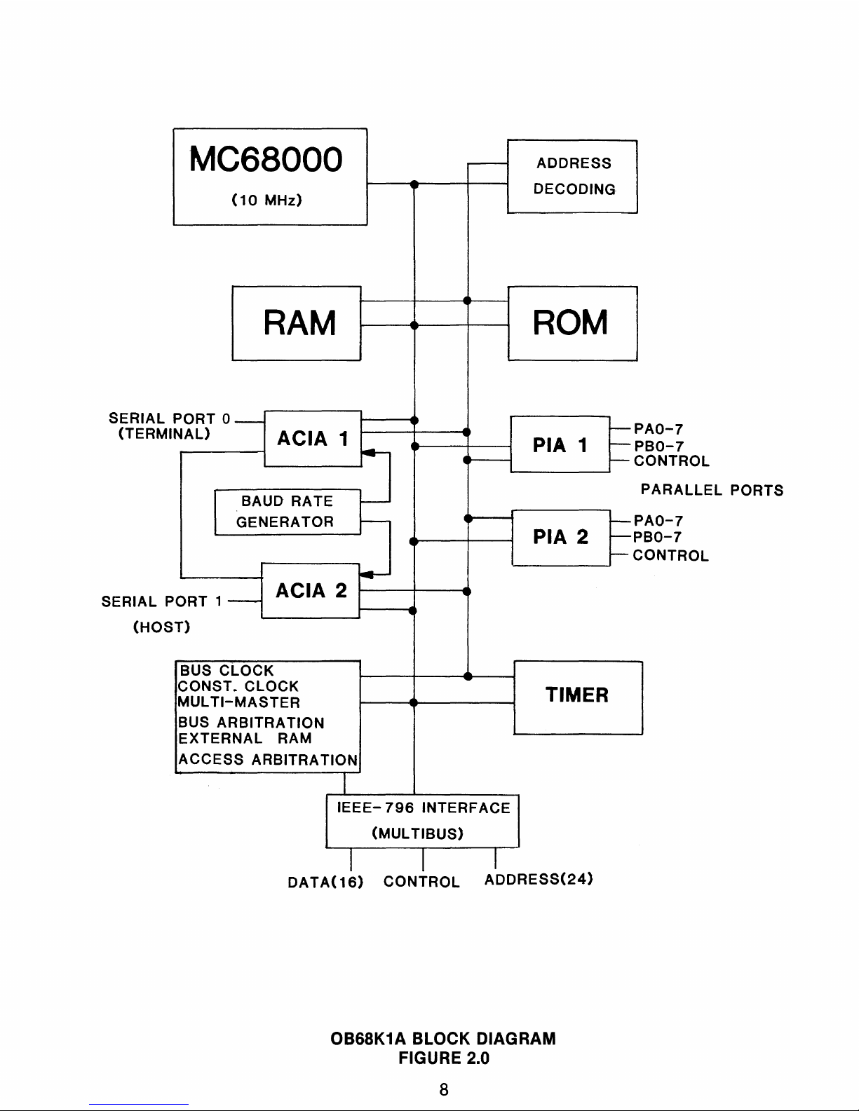
MC68000
(10
MHz)
RAM
SERIAL
PORT
0-
(TERMI
NAL)
ACIA 1
~
BAUD RATE
~
GENERATOR
I-----
~
SERIAL P
ORT
1-
ACIA 2
~
(HOS
T)
BUS
CLOCK
CONST.CLOCK
MUL
TI-MASTER
BUS
ARBITRATION
EXTERNAL
RAM
ACCESS
ARBITRATION
I
ADDRESS
DECODING-
ROM
-PAO-7
PIA 1
-PBO-7
-CONTROL
1...-
__
---1
PARALLEL
PORTS
t--PAO-7
PIA 2
~PBO-7
~CONTROL
'------I
TIMER
IEEE-
796
INTERFACE
(MULTIBUS)
I I 1
DATA(16)
CONTROL
ADDRESS(24)
OB68K1A BLOCK DIAGRAM
FIGURE 2.0
8
Page 14
3.0 GENERAL DESCRIPTION OF OB68K1A
The OB68K1A is designed
to
be both simple and flexible to use. Only general purpose memory and I/O are included on the board. Special purpose facilities such
as disk controllers can
be
added as additional Multibus boards to configure
larger systems.
3.1
Serial Interface
The two asynchronous serial ports are implemented using MC6850 Asyn-
chronous Communication Interface Adapter (ACIA) chips. The baud rates are individually selectable for standard frequencies between
50
and 19,200 baud. The
baud rate selection for each port may be determined either by hardware jumpers
or by software setting. Both ports are factory configured
to
transmit and receive
without handshake lines although jumper options are provided for the normal
CTS,
RTS,
and
DCD
interface signals. All signals are received and transmitted
through
RS232C
compatible buffers. The interface is made through individual,
standarp
26
pin header connectors.
3.2
Timer
A three channel 16-bit timer (MC6840) is available on the board. This timer is in-
tended primarily for processor housekeeping. No connector is provided for input
or output signals to or from the timer - the clock, gate and output pins for each
timer are terminated on wire wrap posts near the chip. For normal applications
the timer counts the processor
"E"
clock, a 1 MHz signal generated by the 68000.
3.3 Parallel Interface
Two
MC6821
Peripheral Interface Adapters (PIA) are provided on the OB68K1A.
All the interface lines are brought outon a standard
50
pin header connector. Five
volt power is also brought to this connector. The
two
8-bit PIA's are configured to
straddle the 16-bit data bus so that 16-bit data may be transferred using the A
ports or B ports
of
both PIA's. Byte operations are supported on both PIA's.
3.4 Bus Arbitration
The bus arbitration circuit allows this computer to share the Multibus with other
processors or mastercontrollers.
RAM
memory that resides on this board may
be
made available
to
other masters on the Multibus. The address
of
the Multibus
port
of
the onboard
RAM
is independently selected.
9
Page 15
3.5 On-Board Memory
3.5.1
On-Board Read Only Memory
The six memory sockets contained on the board are organized as three pairs
of
byte-wide memories. A
minimum
of
64K bytes
of
memory space is always
allocated
for
on-board ROM. However,
for
ROMs
of
less than 64K
bits
each, the
total
ROM
memory space
will
not
be utilized. OnlyEPROM's that are pin compati-
ble with the
pinout
shown in Figure 4.8.4 can be utilized on the OB68K1
A.
Some
compatible
memories are 2716,2732,2764,27128 and 272565 volt only, 24/28 pin
EPROM's containing 2K, 4K, 8K, 16Kand
32
K bytes respectively. Each socket pair
is selected
with
its
base address and range
within
the allocated space arranged
so that the PROM sockets form a
contiguous
blockofmemory. All three socket
pairs
occupy
the same amountofmemory. A small prewired
PC
plug is inserted in
the location provided
to
configure the board
for
various sizesofROM
memories.
Note that 28-PIN sockets are used
for
all ROMstoallow
for
a largerbaseofusable
ROM
chips. The base addressofthe
ROM
is selected as a single memory
block
using
switch
SW-3. Note that although various
ROM
sizes can be accommodated,
all
ROM
sockets
are configured
for
the same
ROM
size. Also see section 3.6.1.
3.5.2 On-Board Dynamic RAM
The OB68K1A has sixteen dynamic RAM chips.
If
configured for 16Kx1 parts, a
total
of
32K bytes are available.Ifconfigured for 64Kx1 parts, a
total
of
128K
bytes are available. The board is offered
with
either the 16K
or
64K parts. The
RAM is selected as a
block
by the main address decoding
circuit
and may be ad-
dressed either in the byte
or
word mode.
The on-board
dynamic
RAM
chips
are accessed and refreshed using
an
LSI
DRAM controller, the DP8409. This 48-pin bipolar
circuit
generates the Row Address Strobes (RAS), Column Address Strobes (CAS), drives the multiplexed address lines, and performs the necessary refresh cycles. Under normal operation
the RAM
controller
receives the processor address strobes and becomes
selected when the asserted address falls
within
the RAM memory space. A
555
clock
generates a
15
us pulse traintoprovide the basic refresh timing. The con-
troller
monitors
both
the
Address Strobe and
its
Chip Select inputs. When a
refresh cycle is needed the
controller
waits
for
an Address Strobetooccur
with
no Chip Select - an
indication
that
the processor is accessing other memory or
I/O. The
controller
will
then perform a
"hidden"
refresh cycle,
that
is, a refresh cy-
cle
that
does not take
time
away from the processor.
If,
during the
15
us period
of
the refresh clock, the RAM is accessed on all Address Strobes, the
controller
will
request the use
of
the bus, cause the processor
to
relinquish the bus and the
RAM
controllerwiII
then perform a forced refresh cycle.
10
Page 16
The duration
of
forced refresh cycle is about
500
ns. Under most conditions the
refresh overhead
of
the OB68K1A will
be
very low. Note that because the entire
RAM
refresh task is implemented in hardware no processor code-execution
cycles are wasted to perform
RAM
refresh by software.
When the processor performs a Multibus cycle, the duration
of
the cycle will
depend on the availabilityofthe bus and the response timeofthe addressed device.
During these offboard cycles, no address strobes are applied to the
RAM
con-
troller
and forced refreshes are then implemented when needed. The XACK signal
output
by
the OB68K1A signals the external master that data from the onboard
RAM has been placed on the Multibus
or
the datatobe
written has been stored.
Shortly thereafter the external master should terminate the cycle by removing the
read or write command. If the cycle is not terminated afterseveral microseconds,
data in the dynamic
RAM
could
be
lost. A timeout circuit is included on the
OB68K1A that interrupts the external access so a refresh can occur. The offboard
master is not required to wait for the completion
of
an
instruction. The LOCK
feature
of
Multibus is implemented so
an
offboard master may do a test-and-set
operation to the onboard
RAM.
Also see sections 3.6.2 and 3.6.4.
3.6
Address Decoding and Memory Mapping
The OB68K1A has been designed so that the memory mapping is switch selectable by the user. No fusible link devices are needed to change the memory map.
Four separate address decoders are included on the board to individually select
the base address
of
onboard
RAM,
onboard
ROM,
I/O and the Multibus access to
the onboard
RAM.
For eachofthese four blocks, the base address is selected by
the setting
of
an
8-bit
DIP
switch. The dip switches have been socketed so that
dip jumpers can
be
used to fix addressing for production purposes, these dip
jumpers are available through OMNIBYTE.
See
section
9.0
for ordering information. The switch setting is compared with the upper address lines to determine
when the various blocks are being selected (SWITCH BIT 1
= L.S.B., SWITCH BIT
o = M.S.B.;
ON
=
0,
OFF =
1).
Much
of
the random logic associated with address decoding and strobe timing has been consolidated into Programmable Array Logic (PAL)* chips. These circuits are programmed
at
the factory andcannot
be
changed
by
the user.
* PAL
is
a trademarkofMonolithic Memories, Inc.
11
Page 17
3.6.1
ROM
Address Selection
(SW-3)
The 8-bit
DIP
switch
(SW-3)
is used to select the base address
of
the onboard
ROM.
Address lines
A16-23
are compared with the switch setting resulting in a
minimum
ROM
block size
of
64K bytes. The minimum block size will accom-
modate memories through 8K bytes per chip. For larger
ROM
chips, larger
memory block sizes
of
128K and 256K bytes may
be
selected by removing
A16
and
A
17
from the comparator inputs, respectively. All the necessary connections are
made by inserting pre-wired plugs in the location provided. Various jumper
models are available from the factory. Note
that
within the
ROM
block, there are
addresses for which no memory exists. For example, using 8K byte PROMs, the
six sockets provided will occupy 48K
of
the minimum 64K byte block size. The
re-
mainder of
this
block is not accessable and cannot
be
assigned to other memory
or devices.
3.6.2
RAM
Address Selection
(SW-1)
The 8-bit
DIP
switch
(SW-1)
is used to select the base address of the onboard
RAM. Jumpers and cut traces at
A15
and A16 are factory configured for either 32K
or 128K RAM. For 32K
RAM
switch
SW-1
selects base addresses on the lower 32K
block
of
64K byte boundary. For 128K
RAM
switch
(SW-1)
selects base address on
128K byte blocks. For 128K
RAM,
BIT 1ofSW-1
is a
"don't
care" bit, since pins
13
and
14
on
U28
are tied together and the cut trace option at A16is opened.
3.6.3 I/O Base Address Selection
(SW-2)
Because the 68000 accesses I/O the same
as
memory, a 64K byte block
of
memory space is decoded and assigned to the I/O space defined in the IEEE
796
bus specification. No options exist on the boardtochange the sizeofthe I/O
address space, but the base address may be located at any 64K byte boundary
within the available
16
megabyte address range. The onboard I/O devices occupy
the uppermost
512
bytesofthe I/O space; all other addresses within the block
default
to
offboard I/O. Table
6.2
gives the addresses of the onboard I/O devices.
3.6.4 EXTERNAL
RAM
Access Address
(SW-4)
A separate 8-bit DIP switch and comparator are used to determine the base
address
of
the onboard
RAM
when that
RAM
is accessed by another Multibus
master. The
RAM
is then accessed at independently selected addresses chosen
to satisfy requirements
of
both the offboard master and the
OB68K1A.Address
line
A15
can
be
used to gate the comparator in order to decode a 32K byte block
size and jumper options allow the block size to
be
increased. Notice that it is
possible to
limit
the amount
of
memory that can
be
accessed from offboard.
12
Page 18
A 128K byte OB68K1A may allow offboard masters to access 32K, 64K or all 128K
bytes
of
its
onboard RAM. This feature allows portions of the onboard
RAM
to
be
protected from otheroffboard masters. Although limiting blocksofRAM
from offboard access is possible, this option has not been implemented by the factory
and should
be
selected by the userifdesired. Also note that in addition to the
jumper and cut trace option on
A16,
pins
13
and
14
on
U31
have been jumpered
and bit 1
of
SW-4
is a
"don't
care" bit.
(See
Section
3.6.2).
3.6.5 Operational Considerations
When the user is setting the base address switches
of
the OB68K1A care must
be
exercised to avoid overlap of the onboard memory spacesofRAM
ROM,
and 1/0.
The offboard access to the dual-ported
RAM
may arbitrarily overlap any
or
all
of
the onboard RAM,
ROM,
or 1/0 space.
In systems that use multiple OB68K1A computers, the onboard base address
selections may
be
the same for all boards.
The external access to the OB68K1A dual-ported
RAM
appears as a simple
RAM
boardtoan
external Multibus Master. Therefore, the base addressofthe external
access
(SW4)must be selected to avoid overlapofthe dual-ported memory space
with any other memory space on the Multibus. External access spaces
of
Multiple
OB68K1A boards must not overlap. The OB68K1A is protected from accessing
its
own
RAM
via the Multibus by negating onboard access while performing offboard
accesses.
3.6.6 Undecoded Addresses
The
OB68K1
A is designed so that all memory accesses default to offboard
Multibus accesses unless the address that is asserted falls within the onboard
RAM,
ROM
or onboard 1/0 space.
3.7
Transfer Acknowledge and Bus Errors
The 68000's data transfers are asynchronous - A Data Transfer ACKnowledge
(DTACK) signal is required to complete
an
access. For Multibus cycles this signal
is provided naturally by the Multibus Transfer ACKnowledge (XACK). For onboard
ROM
cycles, a DTACK generator is provided to terminate the cycle a fixed
time after
an
on-board memory access is started. The delay time is selectable to
match the access time
of
the on-board
ROM
memory chips.
(See
Section
4.3).
The DTACK signal for onboard
RAM
access cycles is also provided
by
the
ROM
DTACK generator and has also been optimzed for the RAM. The OB68K1A must
generate
an
XACK signal when other Multibus masters access the onboard RAM.
This signal serves to terminate the bus cycle for the offboard master. A tap
on
the
ROM
DTACK generator is used to generate this signal at a delayed time that has
been optimized for the offboard
RAM
access time and no user adjustment is per-
mitted.
13
Page 19
When the OB68K1A accesses external Multibus memory or 1/0, the cycle is terminated by the XACK signal returned by the board that was addressed.
In
the eventthat unimplemented off-board memory is accessed, no DTACK will
be
generated.
An
on-board
"watchdog"
timer is included
to
detect a lack
of
response, and a pulse is generated that may be jumperedtothe 68000 Bus Error
input pin. A signal asserted on this pin will initiate bus error exception processing
and a user-supplied routine is executed
to
allow the systemtoanalyze the report
or recover from this condition.
Notice that the 68000 itself will patiently wait forever,
~f
desired, for a DTACK
response to come. No restriction is placed on the speed
of
response
of
the ad-
dressed memory or device. The watchdog timer delay is user determined and its
implementation is optional.
It is included
to
keep the system from hanging up
if
no response is received.
Conditions that will cause a bus error are:
a)
Accesstooff-board memory addresses that have no responding memory (not
plugged in, or not working).
b)
Access
to
oft-board I/O addresses that have no responsing device (not
plugged in, or not working).
An
access to
an
on-board memory address will not cause a bus error evenifa
memory chip is not installed. On-board I/O uses the 68000 synchronous transfer
capability and no DTACK is required.
3.8
Function Codes
The
68000
processor outputs three function code bits,
FCO,
FC1,
and
FC2
that
allow external circuitryto know the internal operating mode
of
the processor. The
~tate
of
these outputsindicates whetherthe processor is in the supervisoror user
state, whether the present access is a program or data reference, or
if
the pro-
cessor is responding to
an
interrupt. The standard configurationofthe OB68K1A
makes use
of
various function code values only to recognize interrupt
acknowledge cycles.
3.9
Clocks
Four clocks are generated on-board.
14
Page 20
3.9.1
Processor Clock
A
10
MHz crystal oscillator provides the processor clock. It connects directly to
the 68000 clock input pin. The
10
MHz clock is also used as the time base for the
DT
ACK generator.
3.9.2 Baud Rate Clock
A 5.0688 MHzcrystal and a COM8116 comprise the baud rate generator. This
baud rate selection can
be
done by setting four jumpers for each serial port, or by
storing the baud rate setting in the COM8116 chip under software control. These
jumper options allow the processor to dynamically control the baud rate
of
either
one or both serial ports.
3.9.3 Bus Clock and Constant Clock
The
10
MHz processor
clock
may
be
used
as
the Multibus BCLK and CCLK.
Because only one card in a Multibussystem can assert these signals,jumpers are
provided
to
remove these clocks from the bus. With these jumpers removed, the
card uses the BCLK and CCLK generated by another master in the Multibus bin.
3.9.4 The E Clock
The
68000
outputs
an
E clock that is one-tenth the processor clock frequency.
Synchronous transfers to the on-board Motorola peripherals are made using this
1MHz clock. Accordingly, it is connected to the enable input
of
the
PIA,
ACIA and
timer chips. This frequency is used by the timer chip when it is configured
to
count the E clock.
3.10
Interrupts
The 68000 provides for seven levels
of
prioritized auto-vectored interrupts. A
74148
priority encoder is included for inputting low active interrupts. The output
of
the 74148 directly connectstothe
IPLO,
IPL1,IPL2 inputsofthe processor.
Interrupts outputs from the on-board peripherals and the Multibus interrupt lines
must be connected to the priority encoder by the user. Wire wrap pins are provided for each interrupt source.
The 68000 feature
of
reading
an
interrupt vector number from the interrupting
device has not been implemented on this board.
15
Page 21
3.11
Status Indicators
Two
LED
indicator lights are included to show when the processor is in the reset
mode (YELLOW) and when the processor is halted
(RED).
312
Single-Step Mode
Circuitry is included on the OB68K1A to implement single step and halt operations. These functions are activated by
an
external momentary contact switch
(for single stepping the processor) and
an
SPST
switch to select the Single Step
or
Run
mode. A 10-pin header on the board may
be
used to connect these switches. Additional signals included on this header are a Reset input, a Non-Maskable
Interrupt input and connections to
LED
drivers for Halt and Reset indicators. This
group
of
signals may be connected to a front panelifdesired.
3.13 Restart Vector Accessing
When a power-on or manual reset
of
the procesor occurs, the processor begins
operation by accessing memory location zero in Supervisory Program space to
load the restart vector and the Supervisor stack pointer. These two vectors must
be
stored in
PROM
because thecontentsofRAM
are unknown at restart time. The
OB68K1A causes the first four memory accesses following a restart to
be
uncon-
ditionally directed to the location 0 through 7
of
the first
ROM
socket pair (IC60
and
IC61).
The access to these
PROM
locations is independent
of
the switch-
selected location
of
ROM
in the address mapofthe OB68K1A. For proper opera-
tion, after restart some memory must exist at location
$000000
in order to have
memory at the addresses where the processor expects to find exception vectors.
This may be either
RAM
or
PROM
and, can
be
in offboard memory.Inany case,
ROM
chips must
be
present in the first two
ROM
sockets, to supply the initial pro-
gram counter and stack pointer values at restart.
3.14 Front Panel Connector
The OB68K1A has a provision for connecting a front panel board that includes
RESET,
SINGLE-STEP, and RUN-STOP switches, HALT and
RESET
LEOS
and a
Software Abort button that asserts NMI, the level
7 interrupt.
An
optional front
panel box and interconnecting cable is available. See Section
9.0
for ordering
information.
16
Page 22
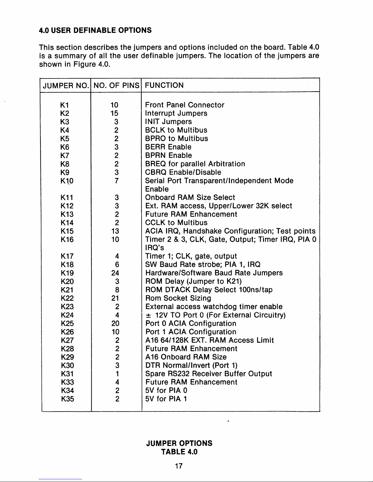
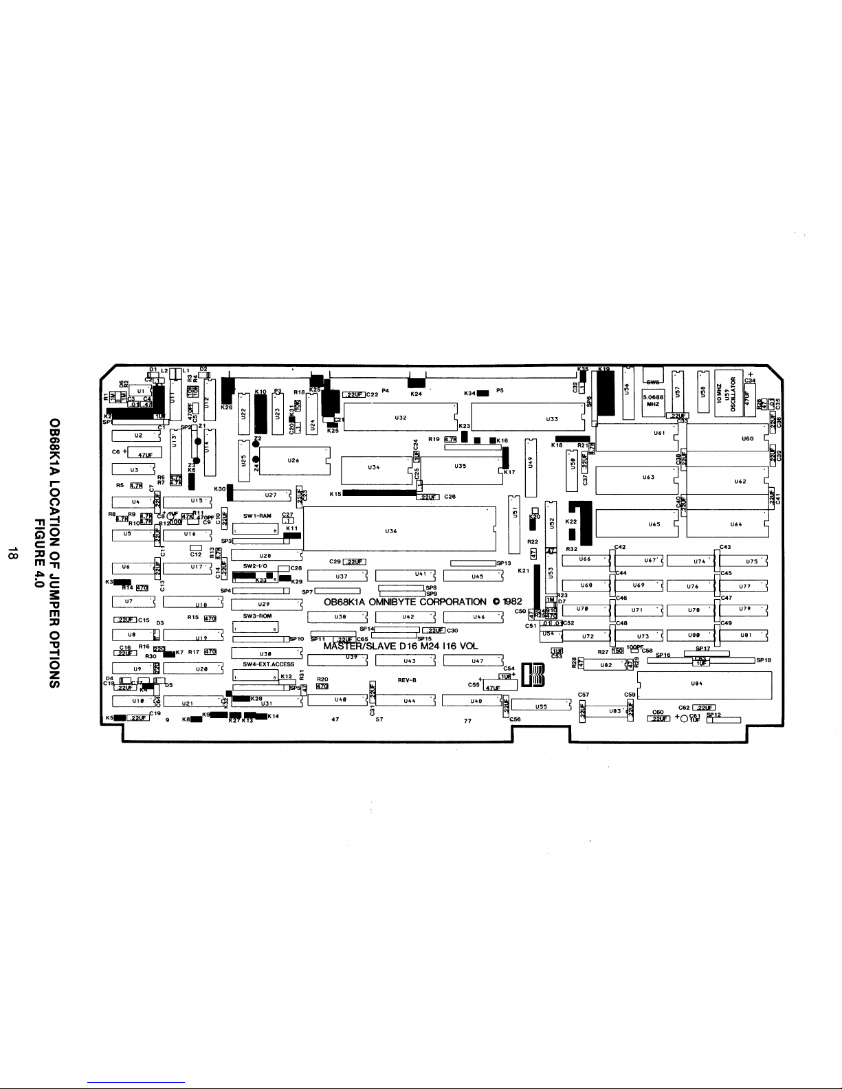
4.0 USER DEFINABLE OPTIONS
This section describes the jumpers and options included on the board. Table
4.0
is a summaryofall the user definable jumpers. The location
of
the jumpers are
shown in Figure
4.0.
JUMPER NO.
NO.
OF PINS
FUNCTION
K1
10
Front Panel Connector
K2
15
Interrupt Jumpers
K3
3
INIT Jumpers
K4
2
BClK
to
Multibus
K5
2
BPRO
to Multibus
K6
3
BERR
Enable
K7
2
BPRN
Enable
K8
2
BREQ
for parallel Arbitration
K9
3
CBRQ Enable/Disable
KlO
7
Serial Port Transparent/Independent Mode
Enable
K11
3
Onboard
RAM
Size Select
K12
3
Ext.
RAM
access,
Upper/lower
32K select
K13
2
Future
RAM
Enhancement
K14
2
CClK
to
Multibus
K15
13
ACIA IRQ, Handshake Configuration; Test points
K16
10
Timer 2 &3,ClK,
Gate, Output; Timer
IRQ,
PIA 0
IRQ's
K17
4
Timer
1;
ClK,
gate, output
K18
6
SW
Baud Rate strobe; PIA1,IRQ
K19
24
Hardware/Software Baud Rate Jumpers
K20
3
ROM
Delay (JumpertoK21)
K21
8
ROM
DTACK Delay Select 100ns/tap
K22
21
Rom
Socket Sizing
K23
2 External access watchdog timer enable
K24
4 ± 12V
TO
Port 0 (For External Circuitry)
K25
20
Port 0 ACIA Configuration
K26
10
Port 1 ACIA Configuration
K27
2
A16 64/128K
EXT.
RAM
Access
limit
K28
2
Future
RAM
Enhancement
K29
2
A16
Onboard
RAM
Size
K30
3
DTR
Normal/Invert (Port
1)
K31
1
Spare
RS232
Receiver Buffer Output
K33
4 Future
RAM
Enhancement
K34
2
5V
for PIA 0
K35
2
5V
for PIA 1
JUMPER OPTIONS
TABLE
4.0
17
Page 23
U64
C43
U74 ' 0
U75
' 5
U76
"0
045
U77 ' 5
0
041
U78
U79
.
5
0
04
•
U8.
U81
' 5
tiE
ISP18
U84
U65
U69 ' 5
L-I
_..::.........:._
U71
. 5
1-1
_
Ll
•
MVCID
.r
l
----J
+
iii
[l
,
Kl0,
R18,K
c;:nm:]C22
P4
K24
K34_
P5
!!!
...
~
~
EJ
~
~g~
LJ
(]
.,.
N
";
.'5
C
__
U_J2
~.,.Ir-----U-JJ--~·.,"'--------1
r---"'-~--~----,"
i:
O
v
R19
IU8 I -
_K16
~
U61
U60
c.
+1
.;l
u"
J
L_~.~()
I
I·...
K18
~R~[5J
~~
UJ
'~R6
1~6:l~'--
---.JJ
UJ4
~~
UJ5
K17:;
~
EJ();
I-----------:..".,~------.....,~()
R5 m ti R7 .
K301
~
1,.If----------.J
,., .
U6J
U62
~I
U""l
U27
"l
Et
.,5
C,.
~
.~m:':.s~~Jb'r'~~
5W1-RAM
ffi.1
'J
~~K~122
I
U5
' 1
U16'
~
'!1
sl
Kll
UJ6
I
••
u
~
~~5Pi
U28
"l
§
••
,
------==---
I
U6
'~.I
U17'
~:!
SW2-I/O
pC28
.--_C_2_9_',_22_UF_1 ISP13 U66
U67'
~
1-1
_
K3.
t3
M
()
•
Ii
K33-sl-K29
1
UJ7
.~
I
U41
'~
U45
'5
K21
4
rn
U SP4J I 1
SP7
1
";1
======:=:-:,
SP=8
1
U7
' 5
lUI
8 . 5 I
U29
. 5 OB68K1A OMNIBYTE CORPoRATION 0
1}82
~C15
03
R15
(tlg
SW3-ROM I
UJ8'5
1 U42
'5
1 U46
'5
U8
lJ
1
'51
I-l
__
~sl
.
SPl~
Icm£JC30
~.10
IffiL
U"
I I
""~;
ISP1M~isSL,WE
D1~5PM24
116
VOL
L22l.EJ
R3~K7
R17
Elm
I
UJ'
~
I1EIl~C58
~-u-9-'mg-IL-
u_2'_.....J'5 SW4-EXT.ACCESS 1
039
'5
1
U4J'5
I
u47'5
[]I~J
~§
.~:,
"~~rl.....lSPZ!:..!.!16L-....!::::~:!rF'=::::L_----.
~~5
L;.!l
...::..s~i
m REV-B
C55+~
111
l
~
[--U2-'--~'~'~,-1
;;;_-=;';_K;;;_28;;=u-J~,~~~~~~--,~..lrJrL..I-_-_-_-_-_U-4~'~~~--,"l~t---u-4-4---"5
1 U48
'5~L..I_--=u:.::.55=--_..J'5
C~5t-7
C59
....
1.------
_
K5_~19
9
K8_K~_-"K14
°
57
~
U8J'~
C60
C62~
Rn"~
47
77
<;;56
1J
C2MJ
+O~~
Ii"M~1
......
2_~
...
-
....
o
m
en
co
"
...A.
»
....
o
o
»
,,::::!
-0
~z
::DO
m"
~c..
oc:
s:
."
m
::D
o
."
::::!
o
z
en
Page 24
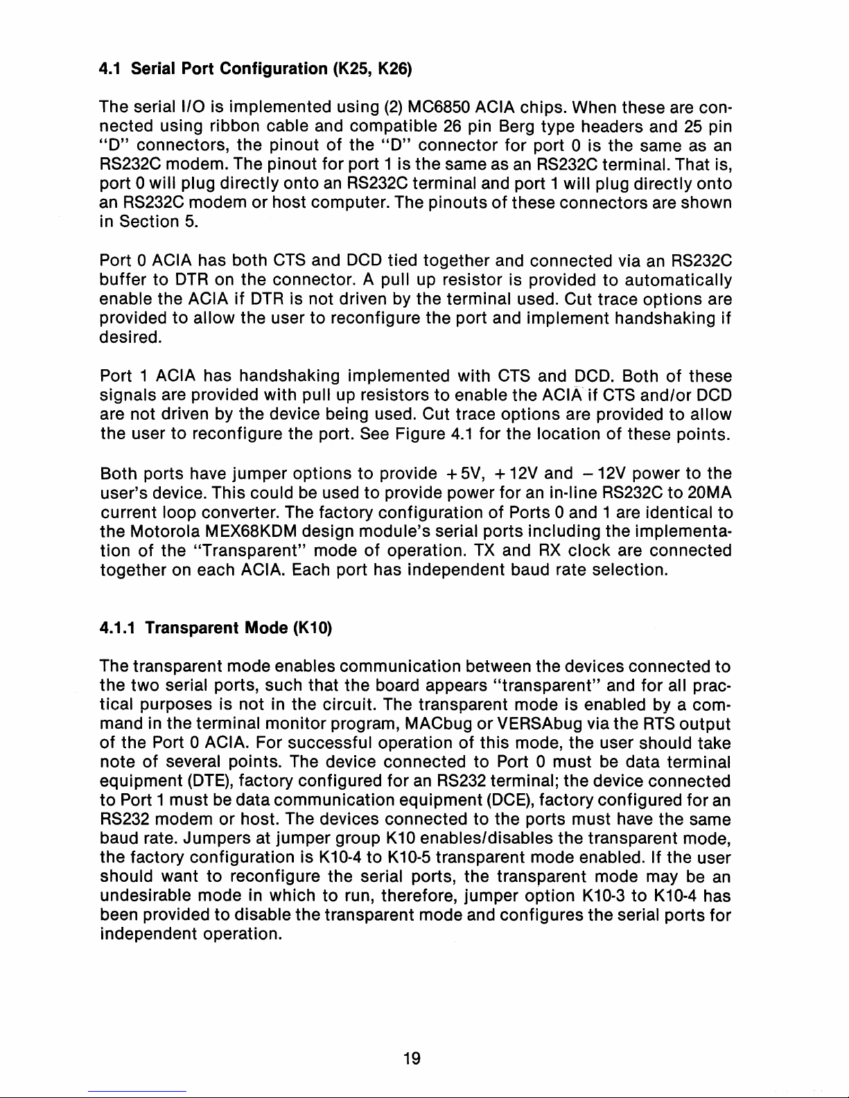
4.1
Serial Port Configuration (K25,
K26)
The serial I/O is implemented using
(2)
MC6850 ACIA chips. When these
are
con-
nected using ribbon cable and compatible
26
pin Berg type headers and
25
pin
"0"
connectors, the pinout
of
the
"D"
connector for port 0 is the same
as
an
RS232C
modem. The pinout for port 1 is the same as
an
RS232C
terminal. That is,
port 0 will plug directly onto
an
RS232C
terminal and port 1 will plug directly onto
an
RS232C
modem or host computer. The pinoutsofthese connectors are shown
in Section
5.
Port 0 ACIA has both
CTS
and
DCD
tied together and connected via
an
RS232C
buffer to
DTR
on the connector. A pull up resistor is provided to automatically
enable the ACIA
if
DTR
is not driven by the terminal used. Cut trace options are
provided
to
allow the user to reconfigure the port and implement handshaking
if
desired.
Port 1 ACIA has handshaking implemented with
CTS
and
DCD.
Both
of
these
signals are provided with pUll up resistors
to
enable the
ACIAif
CTS
and/or
DCD
are not driven by the device being used. Cut trace options are provided
to
allow
the user
to
reconfigure the port.
See
Figure
4.1
for the locationofthese points.
Both ports have jumper options to provide
+
5V,+12V
and -
12V
power to the
user's device. This could
be
used to provide power for
an
in-line
RS232C
to 20MA
current loop converter. The factory configuration
of
Ports 0 and 1 are identical to
the Motorola MEX68KDM design module's serial ports including the implementation of the "Transparent" mode
of
operation.
TX
and
RX
clock
are connected
together on each ACIA. Each port has independent baud rate selection.
4.1.1
Transparent Mode
(K10)
The transparent mode enables communication between the devices connected
to
the two serial ports, such that the board appears "transparent" and for all practical purposes is not in the circuit. The transparent mode is enabled by a command in the terminal monitor program, MACbug or VERSAbug via the
RTS
output
of
the Port 0 ACIA. For successful operation
of
this mode, the user should take
note
of
several points. The device connected to Port 0 must
be
data terminal
equipment
(DTE),
factory configured foranRS232
terminal; the device connected
to
Port 1 mustbedata communication equipment
(DCE),
factory configured for
an
RS232
modem or host. The devices connected to the ports must have the same
baud rate. Jumpers at jumper group
K10
enables/disables the transparent mode,
the factory configuration is
K10-4toK10-5
transparent mode enabled.Ifthe user
should want to reconfigure the serial ports, the transparent mode may
be
an
undesirable mode in which to run, therefore, jumper option
K10-3
to
K10-4
has
been provided
to
disable the transparent mode and configures the serial ports for
independent operation.
19
Page 25
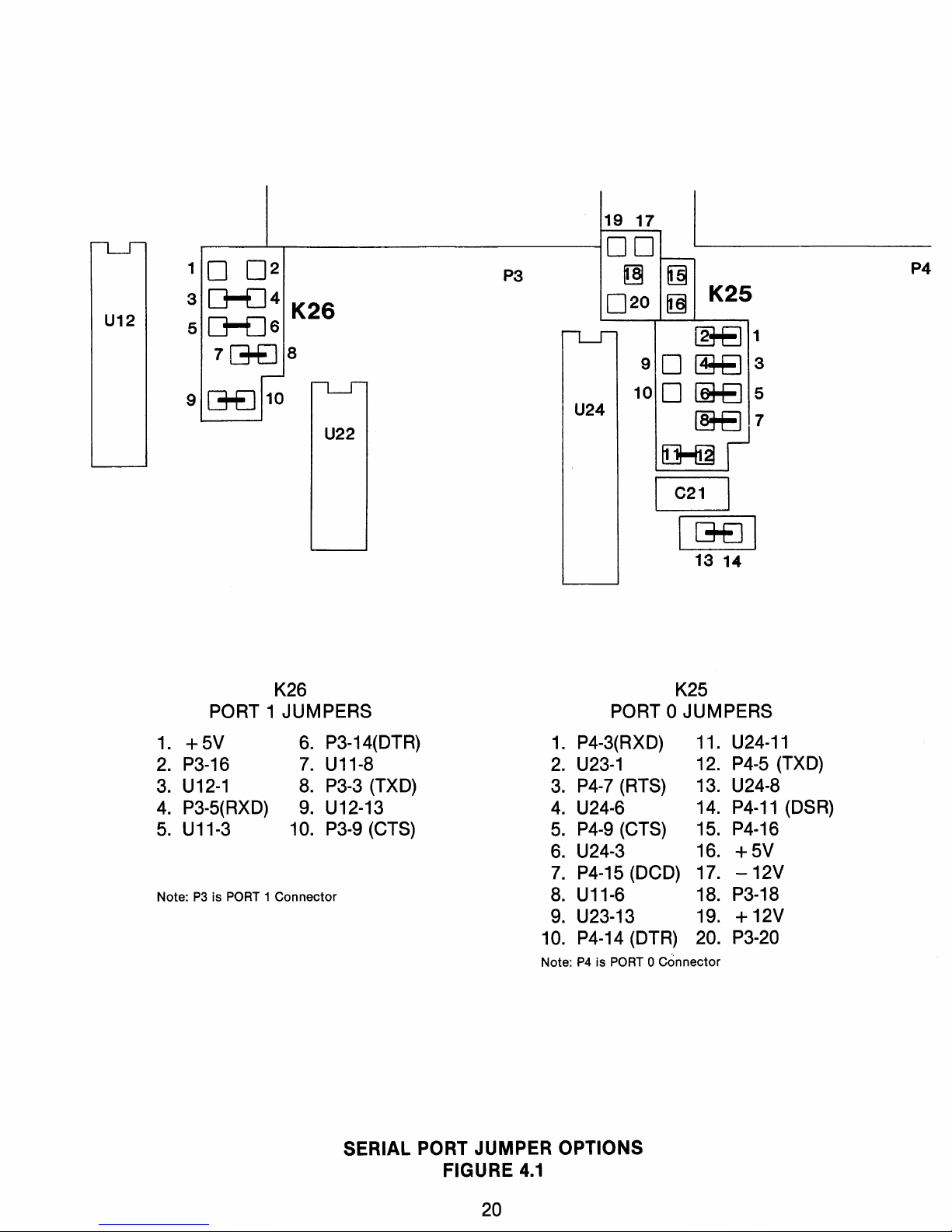
P4
U24
P3
U22
19
17
r-----L---,----------i
0 0
~
[§]
0
20
[§I
K25
[g3-E]
1
90~3
100
~
5
~7
~
I C21 I
I G£J I
13
14
10
0
2
3
[H]4
K26
5
[H]6
7
G-EJ
8
9
G-EJ
10
U12
K26
PORT 1 JUMPERS
1.
+ 5V
6.
P3-14(DTR)
2.
P3-16
7.
U11-8
3.U12-1
8.
P3-3 (TXD)
4.
P3-5(RXD)
9.
U12-13
5.
U11-3 10. P3-9 (CTS)
Note:P3is
PORT
1 Connector
K25
PORT 0 JUMPERS
1.
P4-3(RXD) 11.
U24-11
2.
U23-1
12. P4-5 (TXD)
3.
P4-7
(RTS) 13. U24-8
4.
U24-6 14.
P4-11
(DSR)
5.
P4-9 (CTS) 15. P4-16
6.
U24-3 16. + 5V
7.
P4-15 (DCD) 17.
-12V
8.
U11-6 18. P3-18
9.
U23-13 19. + 12V
10. P4-14 (DTR) 20. P3-20
Note:P4is
PORT
0 Connector
SERIAL PORT JUMPER OPTIONS
FIGURE
4.1
20
Page 26

U22
K10
1~2
3D
:~6
07
U23
K10
1.
U12-4
2.
P3-15(DCD)
3.
GND
4.
U22-13
5.
U27-6
6.
U24-5
7.
U27-5
OPTIONS
4-5
TRANSPARENT MODE ENABLED
3-4
TRANSPARENT MODE DISABLED
5-6
NORMAL
RTS
6-7
INVERTED
RTS
1-2
DCD
TO
PORT
1
NOTE: CHIPS U12 AND U23 ARE RS232 RECEIVERS
CHIPS
U11
AND U24 ARE RS232 DRIVERS
TRANSPARENT IINDEP. MODE JUMPER LOCATION
FIGURE
4.1.1
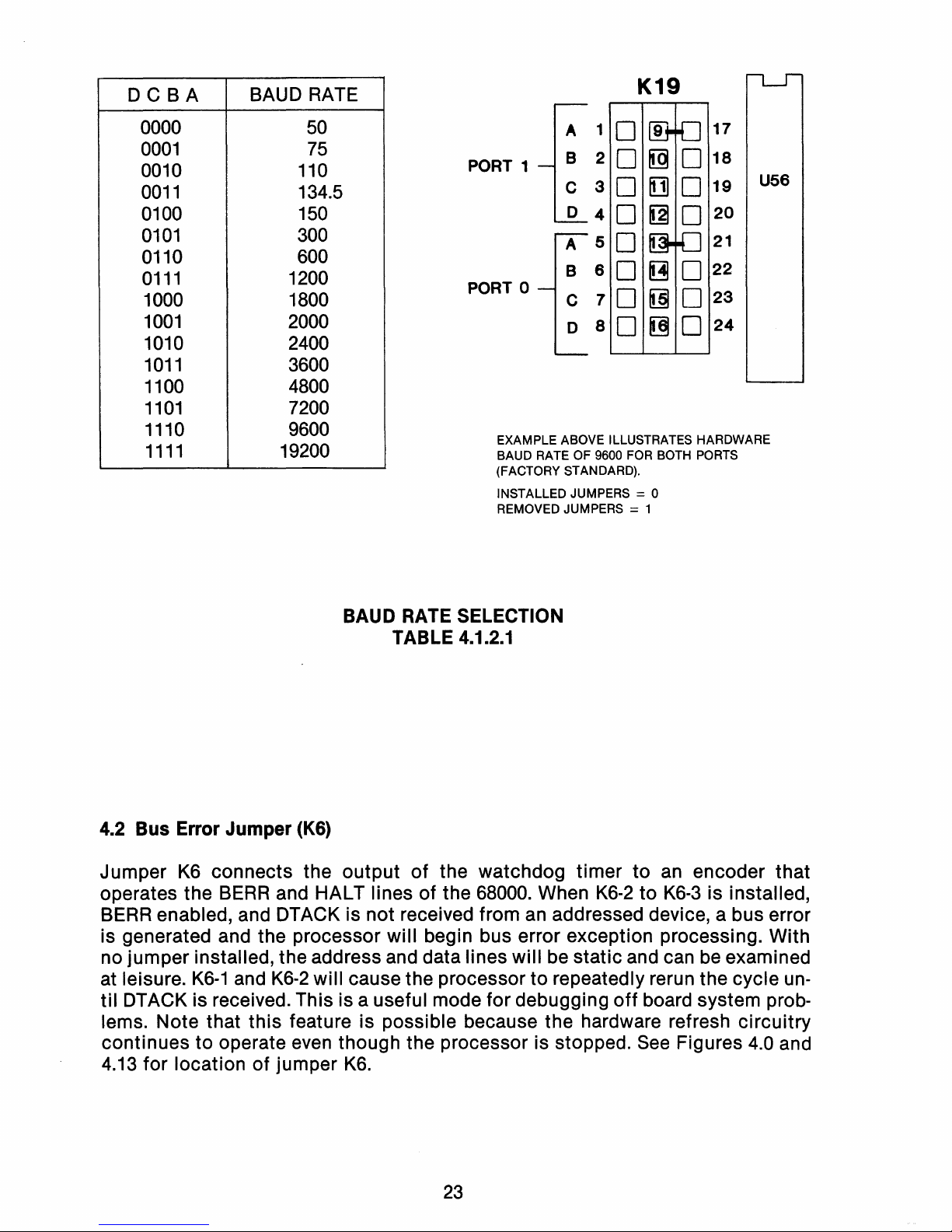
4.1.2 Baud Rate Selection (K18,
K19)
Jumper group
K19
selects the serial baud rate for both Port 0 and Port1.K19
is a
group
of
24
pins arranged in three columns as shown in Figure 4.1.2. The center
row
of
pins connect
to
the baud-rate-setting pins
of
the COM8116 baud rate
generator. The baud rate may
be
set manually or by software.
4.1.2.1
Manual Baud Rate Setting
The center row of pins in jumper group
K19
are pulled up so thatifa particular pin
is not jumpered to ground,
it
will be pulled to a logic1.To select a logiczero, a pin
must
be
jumperedtoground
by
connecting
to
the corresponding pin in the right
hand column. The baud rates corresponding to the possible values
of
the 0,C,B,
and A signals are given in table 4.1.2.1.
21
Page 27
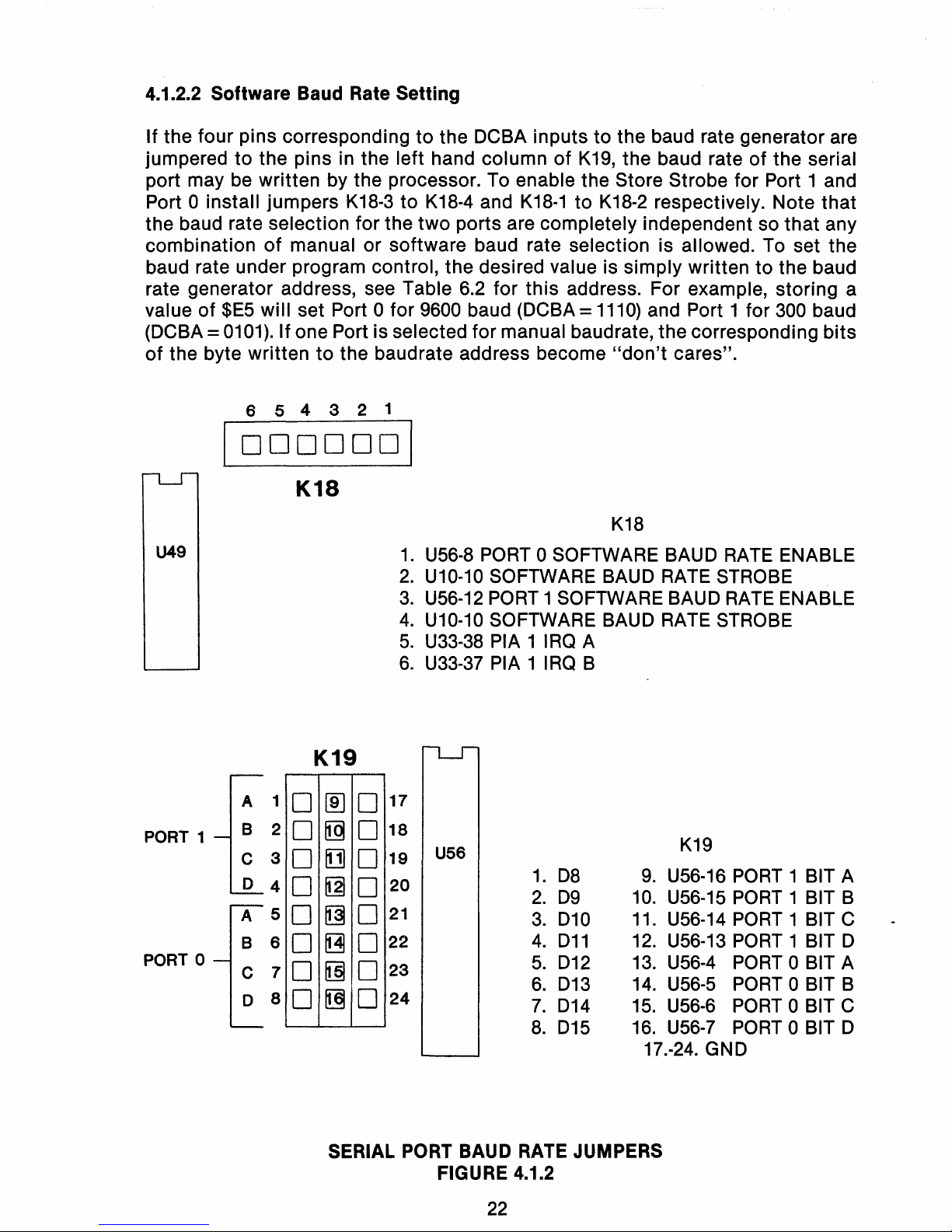
4.1.2.2
Software
Baud Rate
Setting
If the
four
pins
correspondingtothe
DCBA
inputstothe
baud rate generator are
jumpered
to
the
pins
in the
left
hand
column
of
K19,
the
baud rateofthe serial
port may be
written
by
the processor. To enable the Store Strobe
for
Port 1 and
Port 0
install
jumpers
K18-3
to
K18-4 and
K18-1
to
K18-2 respectively. Note
that
the baud rate
selection
for
the
two
ports
are
completely
independent so
that
any
combination
of
manual
or
software
baud rate selection is allowed. To set
the
baud rate under program control,
the
desired value is
simply
writtentothe baud
rate generator address, see Table 6.2
for
this
address. For example,
storing
a
value
of
$E5
will
set Port 0
for
9600 baud (DCBA = 1110) and Port 1
for
300 baud
(DCBA
=0101). If one Port is selected
for
manual baudrate,
the
corresponding
bits
of
the byte
written
to
the baudrate address become
"don't
cares".
6 5 4 3 2 1
10
0
0
000
I
K18
U49
K19
K18
1.
U56-8 PORT 0 SOFTWARE BAUD RATE ENABLE
2.
U10-10 SOFTWARE BAUD RATE STROBE
3.
U56-12 PORT 1 SOFTWARE BAUD RATE ENABLE
4.
U10-10 SOFTWARE BAUD RATE STROBE
5.
U33-38 PIA 1 IRQ A
6.
U33-37 PIA 1 IRQ B
A
1
PORT 1
B
2
C
3
0
4
A
5
B
6
PORT 0
C
7
0
8
0
[[J
0
0
[g
0
0
~
0
0
[g]
0
0
~
0
0
~
0
0
[§]
0
0
~
0
17
18
19
U56
20
21
22
23
24
1.
D8
2.
D9
3.
D10
4.
D11
5.
D12
6.
D13
7.
D14
8.
D15
K19
9.
U56-16 PORT 1 BIT A
10. U56-15 PORT 1 BIT B
11. U56-14 PORT 1 BIT C
12. U56-13 PORT 1 BIT D
13. U56-4 PORT 0 BIT A
14. U56-5 PORT 0 BIT B
15. U56-6 PORT 0 BIT C
16. U56-7 PORT 0 BIT D
17.-24. GND
SERIAL PORT BAUD RATE JUMPERS
FIGURE 4.1.2
22
Page 28
U56
K19
1 0 9
17
2 0
[g
0
18
3 0
~
0
19
4 0 [gl 0
20
A 5 0 21
B 6
0
~
0
22
C 7 0
~
0
23
o 8 0
~
0
24
PORT 1
PORT 0
EXAMPLE ABOVE ILLUSTRATES HARDWARE
BAUD RATE OF 9600 FOR BOTH PORTS
(FACTORY STANDARD).
INSTALLED JUMPERS
= 0
REMOVED JUMPERS
= 1
DCBA
BAUD RATE
0000 50
0001
75
0010 110
0011
134.5
0100
150
0101
300
0110
600
0111
1200
1000 1800
1001
2000
1010 2400
1011
3600
1100
4800
1101
7200
1110 9600
1111
19200
BAUD RATE SELECTION
TABLE 4.1.2.1
4.2
Bus
Error
Jumper
(K6)
Jumper
K6
connects
the
output
of
the
watchdog
timer
to
an
encoder
that
operates the BERR and HALT linesofthe 68000. When
K6-2
to
K6-3isinstalled,
BERR enabled, and DTACK
is
not
received from an addressed device, a bus error
is generated and the processor
will
begin bus error exception processing.
With
no
jumper
installed, theaddress and data lines
will
be
static
and can be examined
at leisure.
K6-1
and
K6-2
will
cause the processortorepeatedly rerun the cycle un-
til
DTACK is received. Thisisa useful mode
for
debugging
off
board system prob-
lems.
Note
that
this
featureispossible because the hardware refresh
circuitry
continues
to
operate even
though
the processor is stopped. See Figures 4.0 and
4.13
for
locationofjumper
K6.
23
Page 29
4.3
DTACK Select (K20,K21)
The DTACK generator
for
the
ROM
consistsofa74164
shift
register that is held in
its
cleared state until either LDS or
UDS
is asserted. Logic ones are clocked
through the
shift
register by the 10MHz (processor) oscillator, and DTACK
timing
is selected by choosing the stageofthe
shift
register connectedtothe DTACK in-
put pin. DTACK is factory
set
for
350ns ROM chips.
If
faster ROM
is
used, the
DTACK
jumper
can be moved
to
provide a
shorter
DTACK delay. Each
jumper
represents
an
incrementof100ns.,
K21-1
being the shortest and
K21-5
being the
longest DTACK delay. (See Figure
4.3)
Notice that the DTACK
timer
is active only
for
on-board
ROM
access. For off-board accesses DTACK is derived from the
Multibus
XACK signal. For on-board
RAM
accesses DTACK is derived from the
RAM
controller
circuitry. Normal onboard
RAM
access will incur no wait states.
See Table 4.3 below. Jumper K20-3 is the
ROM
delay input pin. This pin may be
connectedtovarious delayed
outputsofthe DTACK generator via the
K21
jumper
group. For convenience,
K21-2
is routedtoK20-2
to
become the factory standard
ROM
DTACK delay. A jumperconnecting
K20-2
and
K20-3
provides a
ROM
DTACK
to operate
with
350ns ROMS. For
other
ROM
speeds
K20-3
may be connected
to
other DTACK generator
outputsatK21
accordingtothe delay time given in Table
4.3.If150ns
or
faster ROMS are used, no wait states are required. For zero wait
state operation
for
ROM
memory accesses, connect
K20-3
to
K20-1.
?A
Page 30
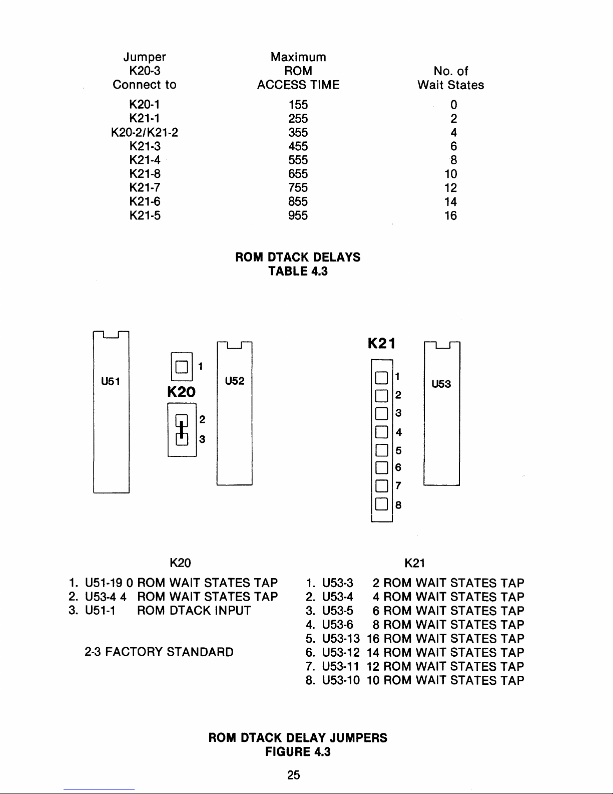
Jumper
Maximum
K20-3
ROM
No.
of
Connect
to
ACCESS TIME
Wait
States
K20-1
155
0
K21-1
255 2
K20-2/K21-2
355
4
K21-3 455
6
K21-4
555
8
K21-8
655
10
K21-7
755
12
K21-6
855
14
K21-5
955
16
ROM DTACK DELAYS
TABLE
4.3
K21
U51
[g]1
U52
0
1
U53
K20
0
2
00:
0
3
0
4
0
5
0
6
0
7
0
8
L-----'
K20
1.
U51-190
ROM
WAIT STATES TAP
2.
U53-44
ROM
WAIT STATES TAP
3.
U51-1
ROM
DTACK INPUT
2-3
FACTORY STANDARD
K21
1.
U53-3
2
ROM
WAIT STATES TAP
2.
U53-4
4 ROM WAIT STATES TAP
3.
U53-5 6 ROM WAIT STATES TAP
4.
U53-6 8
ROM
WAIT STATES TAP
5.
U53-13
16
ROM
WAIT STATES TAP
6.
U53-12
14
ROM
WAIT STATES TAP
7.
U53·11
12
ROM
WAIT STATES TAP
8.
U53-10 10 ROM WAIT STATES TAP
ROM DTACK DELAY JUMPERS
FIGURE 4.3
25
Page 31

4.4 Interrupt Priority (K2)
Interrupts foron-board peripheral chips are terminated on wire wrap posts so that
the user may select the interrupts
to
be
used and the priority level
of
each inter-
rupt. The following interrupts from the onboard peripheral chips are available:
INTERRUPT SOURCE
Port 0 ACIA
Port 1 ACIA
Timer IRQ
PIA 0 IRQ A
PIA 0 IRQ B
PIA 1
IRQ
A
PIA 1 IRQ B
JUMPER
PIN
NO.
K15-11
K15-12
K16-8
K16-9
K16-10
K18-5
K18-6
Because Motorola
IRQ
lines are open drain connections, the interrupt requests
from several chips may
be
wire
ORedtooccupy a single priority level.
The Multibus interrupt lines
(8)
are brought
to
on-board wire wrap posts. These
may also be wire
ORed
and connected
to
the priority encoder inputs'. Both the
Multibus interrupts and the inputs to the priority encoder are located in jumper
group
K2.
See Figure
4.4.
Priority encoder input seven is the highest priority; one is the lowest. Interrupt
requests are not latched on-board. These interrupt requests must be held active until
serviced when they are reset by the processorduring executionofthe interrupt
service routine
as
indicated
by
the IEEE-796 specification.
U1
K2
87654321
00000000
0000000
15
14
13 12
11
10 9
U2
£
K2
P1
CONNECTOR
PROCESSOR
(BACKPLANE) (INT PRIORITY CHIP)
1.
P1-37
INT
4~,
,.,--9.
U2-1
LEVEL 4 IN
PUT
2.
P1-38
INT 5 i
;1{).
U2-2
LEVEL 5 INPUT
3.
P1-35
INT 6
~):~1.U2-3
LEVEL 6 INPUT
4.
P1-36
INT 7;{12.
U2-4
LEVEL 7 INPUT
5.
P1-40
INT 3
1
• (NMI)
6.
P1-39
INT i
1'3.
U2-13
LEVEL 3 INPUT
7.
P1-42
INT
l'
14.
U2-12
LEVEL 2 INPUT
8.·
P1-41
INT 0
15.
U2-11
LEVEL 1 INPUT
INTERRUPT JUMPERS
FIGURE 4.4
26
Page 32

4.5 CCLK and BCLK (K14,
K4)
Jumpers
K14
and
K4
connect the on-board
10
MHz oscillator to the Multibus
CCLK and BCLK lines, respectively. For a single processor system these jumpers
should
be
left in place. For multi-processor systems, only one master should
drive the Multibus
clock
lines. Removing these jumpers will remove the CCLK and
BCLK signals from the bus.
See
Figures
4.0
and
4.13
for
locationofK14
and
K4.
4.6 Bus Arbitration (K5,
K7,
K8,
Kg)
Four jumpers are associated with the bus priority logic.
K5
connects the output
of
the bus arbitration logictothe Multibus
BPRO:k
signal. The trace at
K7
connects
the BPRN* line
to
ground.Ina system with a single bus master,
K7
should be in
place.
In
a Multibus system using serial priority, BPRN* is driven
by
the BPRO*
signal from the master with the next highest priority. For serial operation,
K5
should
be
installed and
K7
should
be
installed for single master or highest priori-
ty
board in a multimaster configuration.
Common Bus Request
(CBRQ)
is a signal that alerts a Multibus Master that
another Master needs
to
use the bus. As shown in Figure
4.6,ifK9
is jumpered
to
connect
K9-1toK9-2,
CBRQ will
be
implemented by the bus arbitration circuitry.
In
this
mode, the OB68K1A will retain ownershipofthe bus until it is forcedtoar-
bitrate with a higher priority user or until a lower priority user asserts CBRQ.
If
another Multibus is not capableofasserting CBRQ the OB68K1A, will relinquish
the bus upon the negation
of
BPRN
and completionofthe present bus cycle. This
allows the OB68K1A to maintain increased
off
board throughput using its CBRQ
feature.
If
K9-2
and
K9-3
are connected, the OB68K1A will relinquish the bus
be-
tween each cycle.
When parallel arbitration is used the
OB68K1
A requests the use of the bus by
asserting
BREQ.
For this modeofarbitration,
K8
should
be
installed.
K8
should
be removed for serial arbitration.
* indicates low active
27
Page 33

U21
2 1
K8~
U10 S I U19 S
2 1 2 1
I
G-£J
I I C19 I I
G-£J
IK7
K5
U20 S
K5 K8
1.
P1-16 (BPRO)
2.
U3-8
JUMPER IN: SERIAL MULTIMASTER
PRIORITIZATION
JUMPER OUT:
PARALLEL MULTIMASTER
PRIORITIZATION
K7
1.
GND
2.
P1-15 (BPRN)
JUMPER IN: SINGLE MASTER
OR
HIGHEST PRIORITY
BOARD IN MULTIMASTER
SYSTEM WITH SERIAL
ARBITRATION
JUMPER OUT:
ALL
OTHER
CONFIGURATIONS
1.
P1-1
(BREQ)
2.
U21-15
JUMPER IN: PARALLEL ARBITRATION
JUMPER OUT: SERIAL ARBITRATION
Kg
1.
P1-29 (CBRQ)
2.
U21-3
3. GND
1-2:
BOARD
MAINTAINS
BUS
CONTROL UNTIL ANOTHER
MASTER REQUEST BUS
2-3:
BOARD RELEASES BUS CONTROL
AFTER EACH TRANSFER
BUS ARBITRATION JUMPER CONFIGURATION
FIGURE
4.6
28
Page 34

4.7 Initialize (K3)
The
master
in a single master system should drive
the
Multibus
INIT line. For
this
type
of
operation
K3-1
should
be
connected
to
K3-2
(See Figure
4.7).
Both the
power-on reset and software generated resets
will
drive the
Multibus
INIT line
(Factory Standard).
For a Multi-Master system,
it
may
be
desirable for INIT
to
be an
input
to
the
OB68K1A board. This is done by connecting
K3-2toK3-3
so
that
the
INIT signal
wi
II
trigger
the
onboard reset generator.
For some
applicationsitmay be necessary for
the
OB68K1Atobe reset
directly
by
the
INIT signal in order
to
synchronize
the
restart sequence
of
multiple
pro-
cessors. To use INIT directly,
cut
the
two
traces Z1-Z3 and Z2-Z4. Connect Pin
K3-2
to
both Z3 and
Z4.
(See Figure
4.13).
This
modification
disables
the
onboard
reset generator and the RESET push button
will
not be operative. The Master driv-
ing INIT
must
meet
the
power-on
timing
requirements
of
the 68000 processor in
order
to
insure a valid restart sequence.
_1J6_S
3 2 1
K31
OG-El I
I
U7
K3
1:
U4-8
RESET OUTPUT
2.
P1-14
INIT
3.
U1-2
RESET GENERATOR INPUT
1-2:
PROCESSOR AND ONBOARD
INIT CIRCUITRY DRIVE
MULTIBUS INIT.
2-3:
MULTIBUS INIT TRIGGERS
ONBOARD INIT CIRCUITRY.
RESET JUMPER CONFIGURATION
FIGURE 4.7
4.8 ROM Socket
Configuration
(K22)
Jumper
area
K22
configures the
ROM
sockets for the
ROM
size
that
is chosen.
Rather than wire wrapping
this
group
of
pins, a small
configurator
board is
plugged in
to
make all the connections simultaneously. The OB68K1A is shipped
withaconfigurator
for
8K(2764's) byte PROMs, but
other
configuration boards are
available from the factory.
29
Page 35

4.8.1
ROM Size
Jumper
Configuration
Figure
4.8.1
shows
the
jumper
group K22 and
identifies
eachofthe pins. The user
may choose
to
wire wrap K22tofield
modify
the
sizeortypeofROM used on
the
OB68K1A.
Normally
the
user
will
use the
factory
supplied
configuration
plugtointerconnect
the K22
jumper
pins. If a
different
PROM type
is
to
be used, the user may
reconnect K22 as shown in Figure 4.8.2. This figure
shows
the
printed
circuit
artwork
for
the
factory
supplied plugs. The user may
choosetofabricate
plugs
or
purchase
them
from Omnibyte. The ROM
sockets
used on
the
OB68K1A have 28
pins.
Thisisto
provide
for
operation
with
certain typesof32K and 64K
ROM
chips.
For operating
with
the24pin devices, ROM's MUST be
installed
with
the unused
pinsonthe
right
sideofthe socket (left justified). See Figure 4.8.3
for
ROM
socket
configuration
and Figure 4.8.4
for
compatible
chip
pinout
configuration.
See sec-
tion
9.0
for
ordering information.
U65
1
2
3
4
5
6
7
8
18 17
DO
[[]
0
~
[g
0
~
0
22
~
0
~
~.
0
~
0
OC§]
0
~
0
K
20
21
19
U52
K22
1.
A 18
2.
A 17
3.
A 16
4.
A 15
5.
A 14
6.
A 13
7.
A 12
8.
A
11
9.
GND
10.
ROM PIN
22
11.
ROM PIN
27
12.
+5V
13. U52-2
14.
U52-1
15.
ROM PIN 2 -A
IL
16. ROM PIN
21
17.
ROM
PIN 26 -
fli]
18.
ROM
PIN
23
19. GND
20.
U30-3
r-
.4
I b
5";<;,)
-)
21.
U30·13 -
.0:;
i 7
NOTE: SEE FIGURE 4.8.2 FOR FACTORY CONFIGURATION
ROM SIZE JUMPER CONFIGURATION
AND
LOCATION
FIGURE
4.8.1
30
Page 36

OBK1A/K22-2716
OBK1A/K22-27128
OBK1A/K22-2732
K22
...
oBK1
AI
K22-27256
K22
0-0
OBK1A/K22-2764
(FACTORY STANDARD)
..
%%%
000-0
0-0
0-0
0-0
000-0
000-0
K22
88
OBK1A/K22-UD
(USER DEFINABLE)
ROM CONFIGURATION PLUGS LAYOUTS
FIGURE
4.8.2
31
Page 37

ODD
BYTE
EVEN
BYTE
IC61
pno
IC60
LOWEST
ADDRESS
IC63
pn1
IC62
IC65
PR2
IC64
HIGHEST
1ADDRESS
ROM SOCKET CONFIGURATION
FIGURE
4.8.3
27256
27128
2764
2732
2716
Vee
Vee
Vee
Al4
PGi
PGi
Al3
Al!
N/C
Vee
Vee
PB
PB
PB
PB
PB
A9
A9
A9
A9
A9
All
All
All
All
Vpp
OE OE OE
OE/Vpp
OE
.-
AlO
AlO
AlO
AlO AlO
CE CE
CE
CE
CE
07
07
07
07 07
(X)
(X)
(X)
(X)
(X)
05
05
05 05
05
ex. ex.
ex.
ex.
04
03
03
03
03
03
PIN
28
27
26
25
24
23
22
21
20
19
18
17
16
15
PIN
27256
27128
2764
2732 2716
Vpp
Vpp
Vpp
Al2
Al2
Al2
AJ AJ
AJ AJ
AJ
NJ NJ
NJ NJ
NJ
AS
AS
AS
AS
AS
M M
M
M
M
A3
A3
A3 A3
A3
lQ
Xl.
lQ
Xl. Xl.
Al Al
Al
Al
Al
NJ
NJ
NJ NJ NJ
00 00
00
00
00
01
01
01
01
01
02
02
02
02
02
God
Gnd
Gnd
Qui
God
PIN NAMES
AO
- A12 ADDRESS LINES
00-07
DATE LINES
CE
CHIP ENABLE
OE
OUTPUT ENABLE
PGM PROGRAM
ROM CHIP PINOUT CONFIGURATION
FIGURE
4.8.4
32
Page 38

4.9
Timer
(K16, K17)
The timer (MC6840) has a clock, a gate and an output for eachofits three timing
channels. All nine
of
these signals are terminated on wire wrap pins in jumper
groups
K16
and
K17.
To operate the MC6840 timer channels, the gate signals
must
be
low.
A trace on the board connects each
of
the three gate signalstoground. A trace
must be cut for the appropriate channel
if
the gate is
to
be
operated from
an
active source.
To use the timer as a programmable interrupt generator for the
CPU,
no external
clock
or gate connections are needed. The MC6840 may use the 1 MHz "E" clock
as a time base. The timer
IRQ
is usually connectedtoa selected priority interrupt
level. See Figure 4.9 for the
PTM
jumper pad locations.
GND GND
I~~OO~
10 9 8 7 6 5 4 3 2 1
,------U35
_~
K16
~
:
o 3
o 4
K17
U49
K17
1.
GND
2.
U35-2
GATE 2
3.
U35-3
OUTPUT 2
4.
U35-4
CLOCK 2
5.
U35-5
GATE 3
6.
U35-6
OUTPUT 3
7.
U35-7
CLOCK 3
8.
U35-9
TIMER
IRQ
9.
U32-38
PIA 0
IRQ
A
10.
U32-37
PIA 1
IRQ
B
1.
GND
2.
U35-26
GATE 1
3.
U35-27
OUTPUT 1
4.
U35-28
CLOCK 1
TIMER OPTION PIN IDENTIFICATION AND LOCATION
FIGURE 4.9
33
Page 39

4.10 External RAM
Access
(K12, K27)
Switch
SW4
is
used
to
set
the
base address
of
the
dual-port RAM
for
offboard
access. Each OB68K1A is set
to
allow
offboard
accesstothe
full
onboard RAM.
For
the
128K version,
the
offboard
access
can be
limited
to
64K bytes by
installing
jumperK27.
The external access can be further restricted
to
a 32K
blockofmemory using
jumper
K12.
The upperorlower
halfofthe
switch
selected
64K base address is chosen by connecting
K12-1
to
K12-2
or
K12-2
to
K12-3
respectively.
Jumper
K12 provides
the
same
function
for
32K versions
of
the
OB68K1A so
that
the
external access can be madetoappear at any 32K byte boun-
dary. Address lines A19-A23 have been pulled
to
logic0to
accommodate systems
that
do
not implement
the
full 16M-byte address. Please note that the 128K RAM
starts
on 128K byte boundaries even if, a lesseramount is made accessibletooff-
board access, ie. upper
or
lower 64K byte blocks.
SW4
321
K12\
000
I
U31
2 1
@§]K27
K12
1.
P1-44
A15 INVERTED = 1
2.
COMPARATOR ENABLE
3.
P1-44
A15 NORMAL =0
2-3:
32K RAM (FACTORY STANDARD
FOR OB68K1A-32K)
NO JUMPER: 128K RAM (FACTORY
STANDARD FOR
OB68K1A-128K)
K27
1.
U31-13
2.
P1-28
A16
NO JUMPER: 32K/128K RAM BOARDS
(FACTORY STANDARD)
JUMPER IN W/128K:
64K EXTERNAL
RAM ACCESS LIMIT
JUMPER
IN
W/32K:
NO EFFECT
NOTE: WITH THE 128K BOARD K27ISNOT JUMPERED AND PINS 13 AND14ON
U31
(ADDRESS COMPARATOR) ARE
TIED TOGETHER. THIS MAKES POSITION 1
ON
SWITCH 4 A DON'T CARE BIT AND REDUCES POSSIBLE
ERRORS.
EXTERNAL RAM ACCESS SIZE JUMPERS
FIGURE 4.10
34
Page 40

4.11
Watchdog Timer for External RAM Access (K23)
In the case
of
a malfunctionofan external Master, an external
RAM
access could
fail
to
terminate a command even after
theXACK
was generated. If thiscondition
would persist for many microseconds, the contents
of
the onboard
RAM
could be
destroyed. Logic is included in the dual port arbitration circuitry
to
negate the
ex-
ternal request
to
the onboard
RAM
after 2.5 micro seconds. Once the access is
terminated by the arbitration circuitrythe board is allowed
to
resume normal pro-
cessing; ie a processor cycle or
RAM
refresh. The external
RAM
access,ifstill
present, is treated as a new request by the arbitration
circuit
and
this
cycle is
repeated. The board is shipped with the watchdog timer enabled, but
this
feature
may be defeated by installing jumper
K23.
See Figure
4.13.
4.12 Optional Front Panel (K1)
Jumper group
K1
is provided as a means
of
connecting a front panel
to
the
OB68K1A. Using the
K1
signals, a front panel can be implemented that includes a
RUN/HALT switch,
RESET,
SINGLE STEP and NMI pushbuttons. The required
ex-
ternal circuitry is shown in Figure 4.12
(B).
The NMI (non-maskable interrupt) may
be
use.d
as a software abort button. This front panel requires only one quad
2-input NAND gate. Power for the front panel is included in the
K1
jumper group.
The front panel circuit
of
Figure
4.12
(B)
is available as
an
option from Omnibyte.
This is a small box with a 5-foot interconnecting cable terminated in a connector
that
plugs
into
jumper group
K1.
The ordering information is given in Section
9.0.
'-----
__
U_1
__
OS
K1
3 0 0 4
5 0
06
70
0 8
9 0 0 10
K1
1.
+5V
2.
GND
3.
HALT LED
4.
MANUAL
RESET
5.
NMIINPUT
6.
RESET
LED
7.
RUN
8.
HALT/SS MODE
9.
SINGLE STEP
PUSH
BUnON
N.C.
10.
SINGLE STEP
PUSH
BUTTON
N.O.
OPTIONAL FRONT
PANEL·
CONNECTOR
FIGURE
4,,12
(A)
35
Page 41

K1
RUN
7
>>-----0
DPST TOGGLE
8>
0
HALT/SS
STEP
NO
10>
0
C DPST MOMENTARY
9>>-----0
NC
NMI
5
7403
DPST
MOMENTARY
4>
RESET
NO
o
C
2
1
6
3
GROUND
+
5V
/ DPST
oNC MOMENTARY
470
HALT
OPTIONAL FRONT
PANEL·
CIRCUIT
FIGURE 4.12 (B)
36
Page 42

4.13 Miscellaneous
Jumper
Identification
Several
jumper
options
have been included on the OB68K1A for
flexibility
and
future enhancement. Although these jumpers are not normally changed by the
user, they are documented in Figure 4.13
for
completeness. The Figure serves
to
define the physical locationofspecific
jumper
pins
that
appear on the OB68K1A
electrical
schematic
diagram. Those
jumper
groups not documented elsewhere
in
the
text
are included in Figure 4.13.
2 1
K41
G-EJ
I
_____
U_1_0
__
S
U13
K6
10
:
~
U15
U14
K4
BUS CLOCK (BCLK) SOURCE TO
MULTIBUS
(P1-13)
NOTE: IN MULTIMASTER SYSTEMS, ONLY ONE BCLK
SOURCE
PER
SYSTEM.
K6
BUS ERROR (BERR)
JUMPER
2-3:
BERR WATCHDOG
TIMER CIRCUITRY
ENABLED.
NO JUMPER: BERR WATCHDOG
TIMER CIRCUITRY
DISABLED.
JUMPER
1-2:
CYCLE
RETRY
(USED
FOR FACTORY
TESTING.)
NOTE: BERR DISABLED IS GENERALLY USED FOR
TROUBLESHOOTING AND
IS
NOT A DESIRABLEMODE TO
RUN
AS ONE COULD GET INTO A STATE THAT WOULD
REQUIRE A RESET.
MISCELLANEOUS JUMPERS LOCATIONS
FIGURE 4.13
37
Page 43

SW1
U31
3 2 1
K111
000
I
'----
__
U28
__
S
K11
ONBOARD RAM SIZE
1~2
32K RAM
2-3128K
RAM
NOTE: FACTORY CONFIGURED, GENERALLY NOT
CHANGED
BY
USER, JUMPER MUST BE IN
PLACE TO ACCESS RAM.
~
12
K13
~
I[3-E]
IK14
K13
JUMPER IN: CONNECTS A18 TO
ADDRESS
COMPARATOR FOR
ONBOARD RAM.
NOTE: K13 IS SUPPLIED FOR FUTURE ONBOARD
RAM ENHANCEMENT.
K14
CONSTANT CLOCK (CCLK) TO
MULTIBUS (P1-31)
NOTE: IN MULTIMASTER SYSTEMS,ONLY ONE
CCLK SOURCE IS PERMITEED.
L-..----
U34
_5
13
12
11
10
9 8 7 6 5 4 3 2 1
K1S1
OOOOOOOOOOG-B-EJ
I
U36
1.
U23-11
(DTR)
2.
U34-24 (CTS)
3. U34-23 (DCD)
4. GND
5.
TEST POINT 2
(TP2)
HALT
6.
TEST POINT 1 (TP1) RESET
7.
TEST POINT 3 (TP3) BERR
K15
8.
TEST POINT 4 (TP4) IPL 2
9.
TEST POINT 5 (TP5) IPL 1
10. TEST POINT 6 (TP6) IPL 0
11. U34-7 PORT 0 IRQ
12. U26-7 PORT 1 IRQ
13. SPARE RS232 RECEIVER
BUFFER INPUT (OUTPUT ON
K31; TTL)
NOTE: K·15 -1,2,3 CONNECTION MADE VIA CIRCUIT BOARD TRACES.
MISCELLANEOUS JUMPERS
LOCATIONS·
CONT.
FIGURE 4.13
38
Page 44

,------U32
_~
K23
rol1
~2
~_U33
_
K23
JUMPER OUT: ENABLES EXTERNAL
RAM ACCESS
WATCHDOG TIMER
CIRCUITRY.
JUMPER
IN:
DISABLES EXTERNAL
RAM ACCESS
WATCHDOG TIMER
CIRCUITRY.
P5
P4
____
I
K24
1"---
_
100
99
1
K24
± 12V TO PORT 0
(FOR EXTERNAL
USE)
1.
- 12V
3.
+12V
2. P4-18
4.
P4-20
1
1
~_2~_1
_U31
__
S
K28
CONNECTS A17 TO ONBOARD RAM
ACCESS COMPARATOR.
NOTE: K28ISSUPPLIED FOR FUTURE RAM
ENHANCEMENT.
MISCELLANEOUS JUMPERS
LOCATIONS·
CONT.
FIGURE 4.13
39
Page 45

SW2-1I0
K29
2 1
1001
i....--
U
_3_
7
S
K29
CONNECTS A16 TO ONBOARD RAM
ADDRESS COMPARATOR
JUMPER IN: 32K RAM
JUMPER OUT: 128K RAM
NOTE: ON 128K RAM BOARDS PINS 3 AND 4 ON
U28
ARE TIED TOGETHER, THUS MAKING POSITION
1 ON SWITCH 1 A DON'T CARE BIT AND
REDUCES POSSIBLE ERRORS.
K30
01
~
:
I_U27---,S
o
o
U23
0
o
o
[Q}K31
o
o
K30
INVERTS SIGN OF DTR ON PORT 1
2-3
NORMAL
(FACTORY STANDARD)
1-3 INVERTED
K31
SPARE RS232 RECEIVER BUFFER
OUTPUT (INPUT ON K15-13; TTL)
MISCELLANEOUS JUMPERS
LOCATIONS·
CONT.
FIGURE 4.13
40
Page 46

SW2-1I0
10
0 0 o
IK33[Q}
5
1
234
K33
CONNECTS A17
(1-2)
AND
A18
(3-4)
TO
ONBOARD RAM ADDRESS
COMPARATOR.
NOTE: K33 IS SUPPLIED FOR FUTURE ONBOARD RAM
ENHANCEMENT.
(35
K34
P5
(FOR EXTERNAL USE)
[8]2
0
1
+5V
FOR PIA 0
2 1
1.
P5-22, 23
I
DO
I
K34
2.
+5V.
K35
~
(FOR EXTERNAL USE)
U33
+5V
FOR PIA 1
1.
+5V
2.
P5-47,48
CUT TRACE OPTIONS
Z1. U25-2 (555
OUTPUn
Z2. U25-2 (555
OUTPUn
Z3. U13-3 (CLR)
Z4. U55-4
SEE SECTION 4.7 FOR
MORE INFORMATION
Z2
O~.
---,
Z1
U14
SIP2
Z3
U25 0
Z4
U26
MISCELLANEOUS JUMPERS
OPTIONS·
CONT.
FIGURE 4.13
41
Page 47

4.14 System Configuration
OB68K1A boards that have been ordered in conjunction with, the OB68K/SYS
Development System or, the three board Functional Board Pack, have been
modified from the standard factory configuration stated earlier in
this
manual.
Port 1has been reconfigured as Data Communications Equipment
(DCE),
so thata
terminal can be connectedtoPort
1.
+ 12V has also been brought
outtothe Port 1
connector and a
T1810*
printer can be connectedtothe Port1.Several interrupts
have also been connected. Listed below are detailsofthe
modifications:
Port 1
Modifications
Jumper
Group
K26
cut
cut
cut
cut
Jumper
Group
K10
cut
P3
connector
Pin11
toPin
15
3-4
5-6
7-8
9-10
1-2
connect
connect
connect
connect
connect
3-8
4-7
6-9
K10-2
to
K25-19
INTERRUPTS
K2-5toK2-13
K2-11
to
K15-11
K2-10
to
K15-12
K2-9
toK16-8
Anode Side
of
06
to
K2-8
5.0 CONNECTOR PINOUTS
wire-wrap
wire-wrap
wire-wrap
wire-wrap
jumper with
IN916-anode
toward
06
Multibus
INT3toLevel 3
INT input
Port 0 IRQ
to
Level
16
INT
input
Port 1 I
RQtoLevel 5 INT
input
Timer IRQ
to
Level
14
INT
input
Isolates INT 0 from
circuitryof555 during
power-on
RESET
5.1
Multibus
P1
and
P2
Connectors
P1
and
P2
are the
Multibus
connectors and are pinned accordingtothe IEEE
796
specification. See Tables
5.1.1
& 5.1.2 respectively for the pin assignments.
*T1810
is a trademarkofTexas Instruments
42
Page 48

(Component Side)
(Circuit Side)
Pin
Mnemonic
Description
Pin Mnemonic
Description
Power
1 GND
Signal GND 2 GND Signal GND
Supplies 3
+5V
+5Vdc
4
+5V
+5Vdc
5
+5V
+5Vdc
6
+5V
+5Vdc
I 7
+ 12V
+ 12Vdc
8
+ 12V + 12Vdc
9
Reserved, bussed
10
Reserved, bussed
11
GND
Signal GND
12
GND Signal GND
Bus
13,
BCLK*
Bus
Clock
--14
INIT*
Initialize
Controls
15
BPRN*
Bus Pri. In
16
BPRO* Bus Pri. Out
17
BUSY*
Bus Busy
18
BREQ*
Bus Request
f§..
MRDC*
Mem Read Cmd
2(l
MWTC* Mem Write Cmd
~-
10RO*
I/O Read Cmd
"22-
~OWC*
I/O Write Cmd
23
XACK*
XFER Acknowledge
24
INH1*
Inhibit
1 (disable RAM)
Bus
25
LOCK*
Lock
26-
JNH2*
Inhibit 2 (disable
PROMorROM)
Controls
""8-,
BHEN*
Byte High Enable
28
ADR16*
and
29
CBRQ* Common Bus
30
ADR17*
Address
Address
Request
31
CCLK* Constant
Clk
32
ADR18*
Bus
33""'
-INIA:,
Intr
Acknowledge
34
ADR19*
Interrupts
35
INT6*
Parallel
36
INT7*
Parallel
37
INT4*
Interrupt
38
INT5* Interrupt
39
INT2* Requests
40
INT3* Requests
41
INTO*
42
INT1*
Address
43
ADR14*
44
ADR15*
45
ADR12*
46
ADR13*
47
ADR10*
Address
48
ADR11
* Address
49
ADR8* Bus
50
ADR9* Bus
51
ADR6*
52
ADR7*
53
ADR4*
54
ADR5*
55
ADR2*
56
ADR3*
57
ADRO*
58
ADR1*
Data
59
DATE* 60 DATF*
61
DATC* 62
DATD*
63
DATA*
Data
64
DATB*
Data
65
DAT8*
Bus
66 DAT9*
Bus
67
DAT6*
68
DAT?*
69 DAT4*
70
DAT5*
71
DAT2*
72
DAT3*
73
DATO*
74
DAT1*
Power
75
GND Signal GND
76
GND
Signal GND
Supplies
77
Reserved, bussed
78
Reserved, bussed
79
-12V
-12Vdc
80
-12V
-12Vdc
81
+5V
+5Vdc
82
+5V
+5Vdc
83
+5V
+5Vdc
84
+5V
+5Vdc
85
GND
Signal GND
86
GND
Signal GND
All Reserved pins are reserved for future use and should notbeusedifupwards compatibility is desired.
IEEE 796
P1
CONNECTOR PINOUT
TABLE
5.1.1
43
Page 49

(Component Side)
(Circuit Side)
Pin
Mnemonic
Description
Pin
Mnemonic
Description
1
Reserved, Not Bussed
2 Reserved, Not Bussed
3
Reserved, Not Bussed
4 Reserved, Not Bussed
5
Reserved, Not Bussed 6
Reserved, Not Bussed
7
Reserved, Not Bussed 8
Reserved, Not Bussed
9
Reserved, Not Bussed
10
Reserved, Not Bussed
11
Reserved, Not Bussed
12
Reserved, Not Bussed
13
Reserved,
Not
Bussed
14
'Reserved, Not Bussed
15
Reserved,
Not
Bussed
16
Reserved, Not Bussed
17
Reserved,
Not
Bussed
18
Reserved, Not Bussed
19
Reserved,
Not
Bussed
20
Reserved, Not Bussed
21
Reserved,
Not
Bussed
22
,Reserved, Not Bussed
23
Reserved, Not Bussed
24
Reserved, Not Bussed
25
Reserved, Not Bussed
26
Reserved, Not Bussed
27
Reserved,
Not
Bussed
28
Reserved, Not Bussed
29
Reserved, Not Bussed
30
Reserved, Not Bussed
31
Reserved,
Not
Bussed
32
Reserved, Not Bussed
33
Reserved,
Not
Bussed
34
Reserved, Not Bussed
35
Reserved,
Not
Bussed
36
Reserved, Not Bussed
37
Reserved,
Not
Bussed
38
Reserved, Not Bussed
39
Reserved,
Not
Bussed
40
Reserved, Not Bussed
41
Reserved, Bussed
42
Reserved, Bussed
43
Reserved, Bussed
44
Reserved, Bussed
45
Reserved, Bussed
46
Reserved, Bussed
47
Reserved, Bussed
48
Reserved, Bussed
49
Reserved, Bussed
50
Reserved, Bussed
51
Reserved, Bussed
52
Reserved, Bussed
53
Reserved, Bussed
54
Reserved, Bussed
Address
55
ADR22*
Address Bus
56
ADR23*
Address Bus
57
ADR20*
58
ADR21
*
59
Reserved, Bussed
60
Reserved, Bussed
All Reserved Pins are reserved for future use and should notbeused if upwards compatability is desired.
IEEE 796
P2
CONNECTOR PINOUT
TABLE 5.1.2
44
Page 50

5.2
PIA and ACIA Connectors
The header connector pin for each signal
of
the PIA,s are shown in Table
5.2.1
below. The
"0"
Columns indicate the pin numbersofa50conductor ribbon cable
is split into
two25conductor sections for termination at the userendofthe cable.
PIN
NUMBERS
SIGNAL
HEADER
*
*
HEADER
SIGNAL
PIAO
PA7
1
1
14
2
PIAO
CB2
PA6
3
2
15
4
CB1
PA5
5
3
16
6
PB7
PA4
7 4
17
8
PB6
PA3
9 5
18 10
PB5
PA2
11
6
19
12
PB4
PA1
13
7
20
14
PB3
PAO
15
8
21
16
PB2
CA2
17
9
22
18
PB1
CA1
19
10
23 20
PBO
NO
CONN.
21
11
24 22
+ 5
VOLTS
+ 5
VOLTS
23
12
25
24
GROUND
GROUND
25
13
1
26
PIA1
PA7
PIA1
CB2
27
14
2
28
PA6
CB1
29
15
3
30
PA5
PB7
\
31
16
4
32
PA4
PB6
33
17
5
34
PA3
PB5
35
18
6
36
PA2
PB4
37
19
7
38
PA1
PB3
39
20
8
40
PAO
PB2
41
21
9
42
CA2
PB1
43
22
10
44
CA1
PBO
45
23
11
46
NO
CONN.
+ 5
VOLTS
47
24
12
48
+ 5
VOLTS
GROUND
49
25
13
50
GROUND
PIA CONNECTOR PINOUT
TABLE
5.2.1
45
Page 51

In Table 5.2.2 and 5.2.3 below, both the header
connector
pin and
the
"0"
pin are
shown
for
each signal on
the
ACIA connectors, becausea 25 pin
"0"
connector
is
normally
installed
on
the
user end
of
the
ribbon cable.
PIN NUMBERS
SIGNAL
HEADER
"0"
"0"
HEADER
SIGNAL
GROUND
1 1
14
2
RX
DATA
3 2
15
4
TX
DATA
5
3
16
6
RTS
7 4
17
8
CTS
9 5
18
10
DSR
11
6
19
12
GROUND
13
7
20
14
DTR
DCD
15
8
21
16
+5VDC
GROUND
17
9
22
18
-12
VDC
GROUND
19 10
23
20
+12VDC
21
11
24
22
23
12
25
24
25
13
26
ACIA CONNECTOR (PORT0)PINOUT (DCE)
TABLE 5.2.2
PIN NUMBERS
SIGNAL
HEADER
"0"
"0"
HEADER
SIGNAL
GROUND
1 1
14
2
TX
DATA
3
2
15
4
RX
DATA
5 3
16
6
7
4
17
8
CTS
9 5
18
"10
11
6
19
12
GROUND
13
7
20
14
DTR
oeD
15
8
21
16
+5
VDC
GROUND
17
9
22
18
-12
VDC
GROUND
19 10
23 20
+12VDC
21
11
24
22
23
12
25
24
25
13
26
ACIA CONNECTOR (PORT1)PINOUT
(OlE)
TABLE 5.2.3
46
Page 52

5.3 Compatible Cable End Connectors
Connector numbers that are compatible
with
the serial and parallel I/O con-
nectors of the
OB68K1
A are given below. For completeness the numbers of the
25
pin
"0"
connectors are also listed.
Serial
1/0
Cable connector for Computer end;
26
pin-
Berg # 65484 -
009
Ansley #
609-2631
&
#
609-2630
Cable connector for Terminal/Modem end;
25
pin
"0"
- Berg # 66167 -
025
Ansley #
609-25P
Parallel
II
0
Cable Connector at Computer end;
50
pin-
Cable Connector at User End,
25
pin
"0"-
Berg #
65484-021
Ansley #
609-5030
&
#
609-5031
Berg # 66167
-025
Ansley # 609-
25P
Note that these are common ribbon cable connectors, and although the part
numbers above are only for the Berg and T
& BIAnsley parts, equivalent con-
nectors are available from several other vendors.
For user convenience, ·Omnibyte can furnish assembled parallel and serial
cables. Order numbers for these cables are given in Section
9.0.
The parallel I/O
cable is a
50
conductor cable terminated in a
50
contact connector at the com-
puter
end,
splitinhalf and terminatedintwo
25
socket
"0"
connectors on the user
end. This arrangement results in two user connectors with the same pinout that
contain all
PIA
0 signals in one connector and all
PIA
1 signals in the other con-
nector.
47
Page 53

6.0 MEMORY DECODING
The IEEE 796
bus
specifications
define
24 address
lines
on
the
backplane and
the
68000 can
support
al124
bitsofaddress. The upper
four
bits
are
brought
out
to
the
P2
connector.
This
makes an
available
address
space
of
16 Megabytes.
Memory
allocation
is
programmable
through
the
use
of
switches
SW-4, SW-3,
SW-2 and SW-1.
6.1
Memory Maps
The
factory
standard
memory
configuration
(MAP1)is
showninthe
diagrams
of
Figure 6.1.1 & 6.1.2.
Switch
settings
for
this
map are:
SWITCH SETTING (ON
=0,
OFF
= 1)
SW-1
RAM BASE ADDRESS $000000 0000 0000
SW-2 I/O BASE ADDRESS
$FFOOOO
1111 1111
SW-3. ROM BASE ADDRESS
$FEOOOO
1111
1110
The MOTOROLA MEX68KDM Design
Module
Memory
Configuration
(MAP
0)
is
showninthe
diagramsofFigure 6.1.3 and 6.1.4.
Switch
settings
for
this
map
are:
SW-1
RAM BASE ADDRESS $000000
SW-2
I/O BASE ADDRESS $030000
SW-3 ROM BASE ADDRESS $020000
48
SWITCH SETTING (ON
=0,
OFF
=1)
0000 0000
0000
0011
0000 0010
Page 54

$000000 -
---,....,..."
.........
_-
*
$000400 -
~"""""'~~~
**
$0007FF
-~~~~~
$007 F80 - """""",-,....,,,,,,,,,,,-,.....,......,.1
$007FFF -
""""""''-''-''-''-''''-''''''I
$01
FFFF
-
~-------'
$020000 -
r---------,
$FDFFFF-'---------'
$FEOOOO
-
1""'7""7'~--r--7'~P"""I
$F
ElF
FF -
f--"-""--'
.............
~:.....t
ON·BOARD
ROM
(64K bytes)
RESERVED
MEMORY
*EXCEPTION VECTORS
**
MACSBUG
RAM
** *
MACSBUG
STACK
****MACSBUG
ROM (8K)
** * *
*ON
- BOARD I/O (.5K)
$FFOOOO
-"""--+t-o---f
OFF-BOARD
NOTE:
I/O
ALL
UNSPECIFIED
(63.5K bytes)
LOCATIONS
ARE
OFF-BOARD
MEMORY
$FFFEOO -
,"",...."...,.....,...-10:,....,.....,--,-1
$FFFFFF
- ** * * *
MAP 1 - 32K bytes RAM (FACTORY STANDARD)
FIGURE 6.1.1
Page 55

$000000 -
*
$000400 -
k""'~r,*"~~
**
$0007FF -
t-'
.............
~-I....--~-"I
$020000 -
r--------,
$FEOOOO
-
.....,....~""2"""'7'..,.....,,....,
****
$007F80 -
~.,.,..,...,.-j-.,.....,.----"
** *
$007FFF -
1'-':....L..L~"""--'-'"'""4
ON-BOARD
ROM
(64K bytes)
(J'I
o
ON-BOARD
RAM
(128K bytes)
$FFOOOO
-
'---r
OFF-BOARD
I/O
(63.5K bytes)
RESERVED MEMORY
*EXCEPTION VECTORS
** MACSBUG RAM
***MACSBUG
STACK
** * *MACSBUG ROM (8K)
** * * *
ON-BOARD
I/O (.5K)
NOTE:
ALL
UNSPECIFIED
LOCATIONS ARE
OFF-BOARD MEMORY
$01FFFF
-
$FDFFFF
--------
$FFFEOO -
~~~:..,-..,~,...
•••••
$FFFFFF
-
~--"-'--~
MAP 1 - 128K byte RAM (FACTORY STANDARD)
FIGURE 6.1.2
Page 56

01
.......
$000000
-".~~.....,......,...--..
$000400
---
*
$0007FF -
**
ON-BOARD
RAM
(32K bytes)
$007F80
-...,..,...,..."..fto-,-
__
-..-l
$007FFF -
***
$020000 -
----,-,.-....,-,
...........
ON-BOARD
ROM
(64K bytes)
$030000
--~---~---~
OFF-BOARD
I/O
(63.5K bytes)
****
$040000
-r----....,
RESERVED MEMORY
*EXCEPTION VECTORS
**MACSBUG RAM
** *MACSBUG STACK
****MACSBUG
ROM (8K)
*****ON-BOARD
I/O (.5K)
NOTE:
ALL
UNSPECIFIED
LOCATIONS ARE
OFF-BOARD MEMORY
$01FFFF
-L-
---I
$03FEOO
--~~~~~
*****
$03FFFF
_~~~~.....a
$FFFFFF-..
----
......
MAP 0 - 32K byte RAM (OPTIONAL)
FIGURE 6.1.3
Page 57

$000000 -
....,...,....,..-.,..~
............
-
$000400
--
*
$0007FF -
**
$007 F80 -
I-,,_....,...Ir
---I
** *
$007FFF -
~--'-'+---"--'-'''''''-I
ON·BOARD
RAM
(128K bytes)
$020000 -
--.,......,....",.........---
$021 FFF -
~1IC.-L--4-L..L.L..L.I
ON-BOARD
ROM
(64K bytes)
$030000 -
~--;..j_---1
OFF·BOARD
I/O
(63.5K bytes)
****
$040000
RESERVED
MEMORY
*EXCEPTION VECTORS
**
MACSBUG
RAM
** *
MACSBUG
STACK
** * *MACSBUG ROM (8K)
*****ON-BOARD
1/0 (.5K)
NOTE:
ALL
UNSPECIFIED
LOCATIONS
ARE
OFF·BOARD
MEMORY
$01
FFFF
-
'--_":"-_~
$03FEOO
-!-r-7"""'7"""'7""-l---r---.o-J
$03FFFF
-
*****
$FFFFFF
-I-----~
MAP 0 - 128 byte RAM (OPTIONAL)
FIGURE 6.1.4
Page 58

6.2
110
Address Assignments
Table 6.2 shows the standard assignment
of
the address space for the onboard
peripherals. The base address is selected by the setting
of
SW-2;
an
8-bit dip
switch
that
determines the upper 8-bits
of
the I/O address.
In
Table
6.2,
XX
represents the upper
two
hexidecimal
digits
determined by
SW-2.
These switches
are normally set at the factory to$FF
to
place the 64K byte I/O block at the upper
end
of
the 24-bit address space. The least significant bits
of
the individual
peripheral registers were chosen to match the addresses
of
the Motorola
KDM
board. These addresses are hardwired and cannot
be
changed by the user.
53
Page 59

ADDRESS
DEVICE
MAIN MEMORY
MODE
DESCRIPTION
ACIA 0
(U34)
$XXFF01
Read
Status
Reg
ister
(MC 6850)
$XXFF01
Write
Control Register
$XXFF03
Read
Receive Data Register
$XXFF03
Write
Transmit
Data Register
BAUD RATE
SELECT (U56) $XXFF10
Write
Baud Rate Register
(COM 8116)
ACIA 1
(U26)
$XXFF21
Read
Status
Register
(MC 6850)
$XXFF21
Write
Control Register
$XXFF23
Read Receive Data
Reg
ister
$XXFF23
Write
Transmit
Data Register
PIA 0
(U32)
$XXFF41
R/W
Data Direction Reg. A (CRA - 2
=
0)
(MC 6821)
$XXFF41
R/W
Peripheral Reg. A (CRA - 2
=
1)
$XXFF43
R/W
Data Direction Reg. B (CRB - 2
=
0)
$XXFF43
R/W
Peripheral Reg. B (CRB
- 2=
1)
$XXFF45
R/W Control Register A
$XXFF47
R/W
Control Register B
PIA 1 (U33) $XXFF40
R/W
Data Direction Reg. A (eRA- 2
=
0)
(MC 6821)
$XXFF40
R/W Peripheral Reg. A (CRA - 2
=
1)
$XXFF42
R/W Data Direction Reg. B (CRB - 2
=
0)
$XXFF42
R/W Peripheral Reg. B (CRB - 2
=
1)
$XXFF44
R/W Control Register A
$XXFF46
R/W Control Register B
PTM
(U35)
$XXFF61
Read
Unused
(MC 6840) $XXFF61
Write
Control Register
#3
(CR2 - 0 =
0)
$XXFF61
Write
Control Register
#1
(CR2 - 0 =
1)
$XXFF63
Read
Status
Register
$XXFF63
Write
Control Register
#2
$XXFF65
Read Timer
#1
Counter
$XXFF65
Write
MSB
Buffer
Register
$XXFF67
Read LSB
Buffer
Register
$XXFF67
Write
Timer
#1
Latch
$XXFF69
Read Timer
#1
Counter
$XXFF69
Write
MSB
Buffer
Register
$XXFF6B
Read LSB
Buffer
Register
$XXFF6B
Write
Timer
#2
Latch
$XXFF6D
Read Timer #3 Counter
$XXFF6D
Write
MSB
Buffer
Register
$XXFF6F
Read
LSB
Buffer
Register
$XXFF6F
Write
Timer #3 Latch
NOTE:xxDETERMINED BY SW-2 (FACTORY SET FF.)
ON·BOARDII0 ADDRESS ASSIGNMENT
TABLE 6.2
54
Page 60

6.3 Motorola MEX68KDM Compatibility
The OB68K1 A can
be
made object code compatible with the Motorola 68000
Design Module. For compatibility, the user should select the following base ad-
dresses: Switch Settings
(ON=0,
OFF =
1)
SW-1
RAM
base address $000000 00000000
SW-2
I/O base address $030000
00000011
SW-3
ROM
base address $020000 00000010
These settings will allow the user
to
execute the MACSbug (MAP
0)
terminal
monitor program and any other MEX68KDM compatible software.
(See
Section
6.1
for Memory Maps).
6.4 OB68K11 OB68K1A Compatibility/Enhancements
The NEW Omnibyte 68000-based OB68K1A Single Board Computer is
an
upgrade
of
the original Omnibyte OB68K1. Although the OB68K1A is
an
extensive
redesign, careful attention has been given to keeping the
"A"
version compatible
with the earlier OB68K1. We believe that complete compatibility has been maintained in the following important areas:
1)
I/O Circuitry.
The same peripheral chips are included- Two 6850 ACIA's, two
6821
PIA's,
one 6840 three channel timer.
2)
Connector Pinout.
The pinout
of
both serial I/O connectors and the parallel I/O connector are the
same as the OB68K1.
3)
Address Decoding.
The
OB68K1
address configuration is available on the OB68K1A.
4)
Software Compatibility.
The OB68K1A maintains software compatibility at the "object code" level.
All programs developed for the
OB68K1
can
be
run on the OB68K1A
without
modification.
In spite
of
the above compatibility, the following important enhancements have
been made:
1)
The on-board
RAM
has been dual-portedtomakeitavailabletoother Multibus
Masters.
2)
An
LSI
dynamic
RAM
controller is used for faster access and increased
reliability.
3)
Ten MHz operation with no wait-states for on-board
RAM
access is possible.
4)
The base addressofon-board RAM,
ROM,
I/O, and external access to on-board
RAM
are all switch selectable. No fusible link PROM's are needed to modify
the address decoding.
55
Page 61

5)
ROM
Socket sizing may
be
determined
by
a configuration plug. No wire-
wrapping is necessary.
6)
Baud rates may be software or manually selected.
7)
Several cut-trace options have been replaced with jumper plugs.
8)
Provision for
an
external Front Panel is included.
9)
On-board single step circuitry is implemented.
10)
Better ground and power distribution have been achieved through the useofa
multi-layer printed circuit board design.
Because
of
the increased speed, users should
be
aware that slight difference
could arise in routines that operate in real time. The 'IE-clock" frequency has
been increased from
800
KHz to 1MHz and time intervals measured by the on-
board MC6840 timer chip will
be
shortened accordingly. Similarly, becauseofthe
increased processor clock frequency and the faster
RAM
access time, software
timing loops will execute faster.
6.5 68000 Memory Organization
Motorola and Intel processors store 16-bit words with the high and low bytes in
the opposite order. Intel words are stored with the least significant byte in the
next higher (odd) location. This organization was induced on Multibus memory
and peripheral cards by defining a 16-bit transfer
to
have the even byte asserted
on data lines 00-07; odd bytes on 08-015.
The 68000 memory organization places the most significant byte in even
ad-
dresses; least significant bytes at the next higher (odd) addresses.
The design criterion placed on this computer board was that bytes placed in byte
addresses will
be
stored at the proper location in memory, and that data, read as
16-bit words, will appear at the 68000 in the correct order. To achieve this goal a
swap byte buffer arrangement is needed
on
the
CPU
card. This design is shown in
Figure
6.5.
Notice that for byte transfers, no problem exists. The bytes are transferred on
00-07 as expected. Only the 16-bit transfers are affected, in which case Multibus
lines 00-07 carry thedata that will arrive at the 68000.as the most significant byte
08-015; a similar swap is made for the least significant byte.
56
Page 62

00-7
LOS
UDS
D8-F
.....
~-4
t-----.DAT8/F/...
--+0----...."
EVEN &
ODD
16
BIT
DATO/-DJ~TF
H
L
MULTIBUS TRANS FE
DEVICE BYTE
BHENI
ADRO/
DATA.PATH
TRANSFERRED
&6
BIT
DEVICE
MULTIBUS
68000
CPU
BOARD
MC
68000
00-7
H
H B BIT
DATO/-DAT7/
EVEN
UDS
D8-F
ATO/7
(]'I
.......
00-7
H
L
8
BIT
DATO/-DAT7/
ODD
LOS
D8-F
SWAP BYTE BUFFER DIAGRAM
FIGURE 6.5
Page 63

6.6 OB68K1A
Schematic
Diagrams
The electrical
schematic
diagrams are shown in Figures 6.6-A, 6.6-B, and 6.6-C.
Factory standard jumper
options
are shown as
dotted
lines in these figures.
"NOTE"
THE FOLLOWING INFORMATION CONTAINS VALUABLE PROPRIETARY INFOR-
MATION WHICH REMAINS PROPERTY OF OMNIBYTE CORPORATION AND
IS
COPYRIGHTED. IT
IS
PROVIDED HERE FOR REFERENCE AND REPAIR
PUR-
POSES ONLY. IT MAY NOT
BE
DUPLICATED FOR ANY REASON WITHOUT THE
EXPRESS WRITTEN PERMISSION OF OMNIBYTE CORPORATION.
58
Page 64

CPU
QM\IBYTE
CORPORATION
(5)
1983
1OF3
OB68K1A
REV-e
74164
:i
II
Ii
I!
Ii
14
4
,
8 7..-._-
.......
"v'V'.
__
...::=..!~'!
T:-_42~j_--=
L~~l=!.J_.~_~
'------=-----+-l-+-----
·------.~cm
f---~..._.---+_f-+-1-+_-.--
.'..---.
NOTE(....)DENOTES
+5V
ALL
DISCRETE·RESISTORS5%TOL
ALLDISCRETE
CAFlICITORS 5 % TeL.
~~--+._----_
..
_--
~~~!==~_.::.:.:_=._
.....
_-_.
OB68K1A
SCHEMATIC·
CPU, BUFFERING AND DECODING
FIGURE 6.6
(A)
Page 65

09
~
o
;j
}.
Jl
..
;;;
I
I
L---
L.--
"
..
..
17
1
21
cso
CAZ
CAl
CB2
C8I
PH7
P86
P85
P84
r:-----
"
PB3
~PB2
PHI
,.;
P80
I;
P117
!!!
All;
P115
PI\4
P113
PAZ
PII'
rl~-
~:~=
.--+-1-
-'='14'-1
RESET
2lI E
i5
:7
I:t'c:
"
..
m
..
~~
AZ..RIO
r~DTR
1 I
II
(~
I
..
tvv::~:':
~I<~RTS
: Q I
N~=
_I
_"
I~I'
L.+++
.:oJ.,
..
.~
I
o=;;Htfl=
.~
..
'II
(J.I
RlCD
~
--
..
17
II
I
-
II
'Ibl~
12:
~
-
~
8~
:JW~
---t
RS~'
o
0025
00
De
24
01
Il2
23
D322Il2
D42t03
OS20
D4
D6
III
OS
(J.I
07 III
D6
1;(J1
07
~
I'
~
~~
TXD
II
~
~
0
RlCIi
,.
R/W
f.!
E~
RS."AI
CSI
10
~
:-
"
IlIQ
!!!
N •
CSO
9ai2
~
~
iii
II~
~
~
lIEl
n
@
~I
;
IW-i
I
C[:~:
'~
M 3 C
~
15
~
4
II
II
lii
Oi
M G~6
9
~
- .
II~
'.
~.
~
II
~;:
:
I~~;
~
2
~:
~~
..
- " !
~
_
K26
.i
MiD.. I i
~II
8 :
.:
2 I
o
II II
!:!
II
I
"I
'
~
_
=~~rN~~
0..
i~DTR
~--1
i
1
112_
0c0
2
:t.
KIO
I
~
3
!:!
t-.
-101
I
~4
m
5 +
~
~~
~
II
1-=--1---'
,
.5!li5
_
~---____,l
..
-
~.~----t-<>--<>-f-1
+12V
-12V
+5V
.
'--+-I+-------~..~
0
inS
•
co
-co •
'I
~I(§
I
(')
~
N
~
~
2i
I
>
--
o
o
m
i
"T1~
'5»
C:(I)
;JJO
m:E:
O)m
0,3:
.-»
m~
--
o
Page 66

~
;:;:
<:iii)
~
AI
A2
n
A4
&!l
&A
A7
AS
..
&ItI
&.,
"'2
.o",
m
AI4
AI!!
.....
......
..
,.,.
All
~
Cft:.
12
CiiCJ
(n:::J
em=:>
GiiiD
emu
IIX47
.-!~=
:jt
62 =
- -
- -
--
-
- -
-
-
==
f
-
--
H~214
t--'--
~-
1:-----
t--~
t--c--
t---c--
~-
~1IDb
~
Dlr-----'
l(:
I*)f---/
~
1:*---'
t:::::
DCi---'
~
013--'
~
Dlf---'
~
DIIIf---'
1114
74
75
7G
77
78
79
80
81
5
-.0
tcJ
NJ
~
~
:--
~
~
tc
~
orr~
Il2II
AI
~
',:!~Q
b
A2
~
E
~
~ ~
54
II
410
All
C:
~
IN.
1M
P
M
~
te:
fS
E E
.47U1"
~.4
'I
!I5lI
All
C:
~
~+
~
All
~
E
~
~ ~
lIV
lIf~
ClI2
A7
C:
C:
~
ClIO~K!2
.01
"-
AlI
"-
'--
'--
"'---
'-==
.01
~ ~
'--
-
'---
~
~
- -
....I-
Ot.NBYTE
CORPORATION
01983
aOFa
0f368K
1A
FEV-e
OB68K1A
SCHEMATIC·
MEMORY
FIGURE 6.6
(C)
Page 67

PART
# OF
NUMBER DESCRIPTION
PCS.
LOCATION
OB00406CN
26
PIN RIGHT ENC. HEADER
2
P3,4
OB00409CN
50
PIN RIGHT ENC. HEADER
1
P5
OBOO093CP
270
pF
CAP
3
C28,
C58,C64
OB00916CP 470
pF
CAP
5
C5,9,12,
17,21,
OB00103CP
.01
uF CAP
4
C3,
35,
51,
52,
OB00104CP
.1
uF CAP
8
C2,
20, 24, 25, 27,
32
53,
54
OB00105CP .47
uF
CAP
2
C4,50
OB00106CP 1.0
uF
CAP
2
C8,61
OBOO110CP
47
uF
CAP
3 C6,
34,
55
OB00881CP .22 uF CAP
36
C7,
10,
11, 13, 14, 15,
16, 18,
19,
22,
23, 26
29,30,31,33,36,37
38,39,40,41,42,43
44,45,46,47,48,49
56,57,59,60,62,65
OB00108CP 10 uF CAP
1
C1
OB00912CP 1 uF CAP (CERAMIC)
1
C63
OB00134DI IN4003
2
01,2
OB00137DI IN916 5
03,4,5,6,7
OB00153LE LED (RED)
1
L1
OB00835LE
LED (YELLOW) 1
1..2
OBOOO08RE
47
OHM 1/4W RESISTOR
5
R22,
26,
28,
29,
31,32
OBOO011RE
100 OHM 1/4W
1
R12
OBOO013RE
150 OHM 1/4W
1
R27
OBOO015RE
220 OHM 1/4W
2
R16,
30
OBOO018RE
470 OHM 1/4W 5
R14,
15, 17,
20,
25
OBOO035RE
4.7K OHM 1/4W
9
R5,6,
7,8,9,10,13
19,21
OBOO042RE
10K OHM 1/4W 3
R3,4,18
OBOO049RE
47K OHM 1/4W 1
R11
OBOO053RE
1M OHM 1/4W 3
R1,2,23
OB00919RE 910 OHM
1/4W 1
R24
oB00529SA
2 PIN STRIP 7
K4,5,7,8,14,
20,
23
oB00586SA 8 PIN STRIP 5
K2,
19,
19,
19,
21
oB00587SA
10 PIN STRIP
1
K16
oB00649SA
7 PIN STRIP 1
K2
OB00681SA
13 PIN STRIP
1
K15
OB00759SA
3 PIN STRIP 6
K3,
6,9,10,11,12
OB00760SA
4 PIN STRIP 1
K17
oB00808SA 5 PIN STRIP 2
K1,
1
OB00914SA
6 PIN STRIP
1
K18
OB00921SA
1 PIN STRIP 2
K20,32
OB00931SA 6 PIN STRIP
2
K22, K22
OB68K1A PARTS LIST
TABLE 6.6
62
Page 68

PART
# OF
NUMBER
DESCRIPTION
PCS.
LOCATION
OB00932SA 2 PIN STRIP
1
K22,
OB00933SA 4 PIN STRIP
2
K22, K22
OB00377SK
64 PIN SOCKET
1
U36
OB00379SK
14 PIN SOCKET
1
U57
OB00380SK 16 PIN SOCKET
20
U66-U81, SW1-SW4
OB00381SK
18 PIN SOCKET
1
U56
OB00382SK
20 PIN SOCKET
6
U18, 20, 21, 49,
51,
55
OB00384SK
24
PI
N SOCKET
2
U26, 34
OB00385SK
28
PI
N SOCKET
7
U35, U60-65
OB00386SK
40
PI
N SOCKET
2
U32, 33
OB00574SK
48
PI
N SOCKET
1
U84
OB00812SK
INDIVIDUAL SOCKET PIN
4
U59, 59,
59,
59
OBOO063SP
4.7K
OHM
6 PIN SIP
1
SP2
OBOO064SP
4.7K OHM 10 PIN SIP
1
SP1
OBOO065SP
47K OHM 8 PIN SIP
10 SP7,
8,
9,11,13,14
15, 16, 17, 18
OB00848SP
22K OHM 6 PIN SIP
1
SP12
OB00882SP
470 OHM 10 PIN SIP
1
SP5
OB00913SP 47K OHM 10 PIN SIP
4
SP3,
4,
6,10
OB00163SW
PUSH BUTTON SWITCH (N.O.)
1
SW5
oB00834SW
8 POSITION SWITCH
4
SW1,
2,3,4
OB00149XT
5.0688 MHz CRYSTAL
1
OB008131C
7400
1
U22
OB008141C
7404
2
U7,
25
OB008151C
7407
1
U4
OB009971C
74F08
1
U83
OB008171C 74LS30
1
U5
OB008181C 7432
1
U3
OB00920lC
74S32
1
U82
OB008191C
74S74
3
U50, 57, 58
OB00820lC
74LS77
1
U8
OB002161C
74123
1
U16
OB008211C
74LS125
1
U9
OB008221C
74128
1
U10
OB008231C
74LS138
3
U15, 17, 52
OB008241C
74LS148
2
U2,
13
OB008251C
74LS164
2
U6,53
OB008261C
74LS279
1
U14
OB008271C
74LS640
7
U27, 38, 39, 40, 43, 44,
48
OB008281C
74LS645
6
U37, 41, 42,
45, 46,
47
OB68K1A PARTS
LIST·
CONT.
TABLE 6.6
63
Page 69

PART
# OF
NUMBER
DESCRIPTION
PCS.
LOCATION
OB008291C
74LS645-1
1
U19
OB00830lC NE 555 2
U1,54
OB008311C 74LS686
4
U28, 29, 30,
31
OB008321C
MC1488
2
U11,24
OB008331C MC1489
2
U12, 23
OB003641C
PAL 16L8
4
U18,_
20,51,55
OB005851C
PAL 16R4
2
U21, U49
OB003381C
MC6821
2
U32, U33
OB003421C
MC6840
1
U35
OB003471C
MC6850
2
U26, U34
OB003571C
MC68000L10
1
U36
OB002551C
COM8116
1
U56
OB002631C
DP8409(-2)
1
U84
OB00690lC
64K X 1
DRAM
(128K)
16
U66-81
OB005991C
16K X 1
DRAM
(32K)
16
U66-81
OB00761XT
10
MHZ
OSCILLATOR
1
U59
OB00809JP JUMPER (128K)
13
STD. CONFIGURATION
(32K)
14
STD. CONFIGURATION
OB00923SA
JUMPER KIT (17 JUMPERS)
USER JUMPER OPTIONS
OB00501CE
BLUE CARD EJECTOR
2
OB68K1A PARTS
LIST·
CONT.
TABLE 6.6
64
Page 70

7.0 TERMINAL MONITOR PROGRAMS
Two terminal monitor programs are available from Omnibyte for use with your
OB68K1A. These programs are licensed for distribution from Motorola Inc. by
Omnibyte and are provided
as
object code in
PROM.
Both programs include the
source listings
of
initialization and
I/O
routines.
OB68KMACS is
an
8K byte firmware monitor which provides for memory examination, program loading and controlled program execution. It provides the user with
the capability to connect a terminal
to
the OB68K1A single board computer and
communicate with the board. It provides a vehicle to initialize and configure the
on-board I/O devices, examine the MC68000 registers, and perform various other
functions
of
this powerful monitor as listed in the command summary.
OB68KMACS is essentially Motorola's MACSbug firmware monitor program
designed for the MEX68KDM design module.
OB68KVERSA is a 16K byte firmware monitor/debugger which provides the user
with all the functions
of
MACSbug, described above, and has been extendedtoinclude a single line assembler/disassembler; block move, block test, block initialize capabilities and a Help menu.
OB68KMACS and OB68KVERSA are available in the OMNIBYTE factory standard
memory configuration (MAP
1)
or the Motorola MEX68KDM DESIGN MODULE
memory configuration (MAP
0).
65
Page 71

8.0 WARRANTY INFORMATION
All boards manufactured and sold by Omnibyte Corporation are warranteed
against defects in materials or workmanship and are guaranteedtomeet specificationsineffect
at the
timeofmanufacture for a periodof(2)
years from the date
of
delivery.
Omnibyte's responsibility under
this
warranty is limited
to
repair or replacement
of
any item (at our option) returned
to
the factory during the warranty period,
postage prepaid. Omnibyte shall either repair
or
replace the item, provided that
the failureofthe item, in
our
opinion, was not duetoabuse,
modification
or acts
of
God. EXCEPT
AS
OTHERWISE INDICATED, THERE ARE NO OTHER WARRAN-
TIES, EXPRESSED
OR
IMPLIED, INCLUDING, BUT NOT LIMITED
TO,
IMPLIED
WARRANTIES OF MERCHANTABILITY
OR
FITNESS FOR A PARTICULAR
PUR-
POSE.
Omnibyte's liability shall be limited
to
the purchase price
of
the item
or
items, and Omnibyte shall not be responsibleorliable
for
any'lost
profitsorcon-
sequential damages, or
for
any claim against the purchaser by any party.
"NOTE"
ALL BOARDS BEING RETURNED
TO
OMNIBYTE CORPORATION FOR REPAIR
MUST
BE
ACCOMPANIED WITH A RMA NUMBER (RETURN MATERIAL AUTHOR-
IZATION). THIS NUMBER WILL
BE
ISSUED
TO
YOU
BY
OMNIBYTE WHEN
RE-
QUESTING AUTHORIZATION
TO
RETURN
YOUR BOARD. ALSO,
AN
EXPLANA-
TION OF THE PROBLEM AND NAME AND PHONE NUMBER OF THE PERSON
USING THE BOARD WHEN PROBLEM OCCURED SHOULD
BE
ENCLOSED WITH
THE RETURNED BOARD. THIS PROCEDURE WILL HELP
US
TO
SPEED
UP
THE
REPAIR AND RETURN OF YOUR BOARD.
ANY BOARDS RECEIVED
BY
OMNIBYTE CORPORATION WITHOUT A RMA
NUMBER WILL
BE
RETURNED
TO
SENDER, AT THEIR EXPENSE, UNTIL A RMA
NUMBER HAS BEEN OBTAINED FROM OMNIBYTE.
66
Page 72

9.0 ORDERING INFORMATION
Order numbers forthe OmnibyteOB68K1A computer, Monitorprograms and
ROM
size configuration plugs and other accessories are as follows:
32K
RAM
Computer
OB68K1A-32K
128K
RAM
Computer
OB68K1A-128K
MACSBug in 8K X 8
PROMS
MAP0
(See
Section
7.0)
. . . . . . . . . . . . . . . . .. . .. . ...OB68KMACS-
64
- 0
MAP 1
(See
Section
7.0)
OB68KMACS-64-1
VERSABug in 8K X 8 PROMS
MAP 1
(See
Section
7.0)
. . . . . . . . . . . . . . . . .. . .. . ...OB68KVERSA-
64-1
MAP 0 (See Section
7.0)
OB68KVERSA
~64
- 0
ROM
Configuration Plug for
2716
OBK1A/K22-2716
2732
-
OBK1A/K22-2732
2764
OBK1A/K22-2764
27128
OBK1A/K22-27128
27256
OBK1A/K22-27256
User-definable
ROM
Configuration Plug
OBK1A/K22-
UD
Optional Front Panel Box
w/5'
cable OB68K1AFPM
Serial I/O Interface Cable Assy.
-10'
long OB68K1S1C
Parallel I/O InterfaceCable Assy. -
5'
long
OB68K1
P1C
DualInLine Shunt OB01049CN
Omnibyte's terms are: NET
30
DAYS with approved credit. The F.O.B. point is:
West Chicago, Illinois. Items will be shipped: United Parcel Service surface
unless otherwise instructed.
10.0 APPENDIX (DATA SHEETS)
The following pages contain excerpts from the data sheets ofJhe OB68K1A on-
board devices. Familiarity with the operating characteristics of these devices will
be
necessary for proper operation and are included for that purpose. They have
been reprinted courtesy of Motorola, Inc.
The reprints contained herein are the most current available at the time
of
print-
ing and may
be
updated by Motorola, Inc. without notice at any time. Omnibyte
assumes no liability for notifying purchasers
of
this manual of these updates.
67
Page 73

®
MOTOROLA
SEMICONDUCTORS
3501EDBLUESTEIN
BLVD.,
AUSTIN,
TEXAS
78721
Advance
In:forIllation
16-BIT
MICROPROCESSING
UNIT
MC68000L4
(4
MHz)
MC68000L6
(6
MHz)
MC68000LS
(8
MHz)
MC68000Ll0
(10
MHz)
05
D6
07
D8
D9
D10
D11
D12
D13
D14
015
. GND
A23
A22
50
A21
49-·,·,
VCC
48 A20
47 A19
46 A18
45 A17
44 A16
43 A15
42
A14
41
A13
'10
A12
39
A11
38 A10
37
A9
36
A8
35
A7
34
A6
33
5
PIN
ASSIGNMENT
L SUFFIX
CERAMIC
PACKAGE
CASE
746
HMOS
(HIGH-DENSITY, N-CHANNEL,
SILICON-GATE DEPLETION LOAD)
l6-BIT
MICROPROCESSOR
D4
D3
D2
D1
DO
AS
UDS
lDS
R/W
DTACK
BG
BGACK
BR
VCC
ClK
GND
HALT
RESET
VMA
E
VPA
BERR
IPl2
IPl1
IPlO
FC2
FC1
FCC
A1
A2
A3
A4
PROGRAMMING MODEL
31
1615
87
0
DO
01
D2
D3
Eight
D4
Data
Registers
D5
D6
D7
31
1615
0
I
AO
I
A1
I
A2
Seven
I
A3
Address
I
A4
Registers
I
A5
A6
r-
- - -
-User
Stack
~inter-
- -
--1
Two Stack
Supervisor Stack Pointer A7
Pointers
L
- -
_____________
.J
31
0
I
I
Program
Counter
15
87
0
Status
ISystem Byte:
User Byte
I
Register
Advancesinsemiconductor technology have provided the capability
to place on a single silicon chip a microprocessor at least
an
order
of
magnitude higher in performance and circuit complexity than
has
been
previously available. The MC68000isthe firstofa familyofsuch VLSI
microprocessors from Motorola. It combines state-of-the-art
technology and advanced circuit design techniques with computer
sciences to achieve
an
architecturally advanced 16-bit microprocessor.
The resources available to the MC68000 user consist
of
the following:
• 32-Bit Data and Address Registers
•
16
Megabyte Direct Addressing
Range
•56Powerful Instruction Types
• OperationsonFive
Main Data Types
• Memory Mapped
I/O
•14Addressing Modes
As shown
in
the programming model, the MC68000 offers seventeen
32-bit registers
in
additionto
the 32-bit program counter
and
a 16-bit
status register. The first eight registers (00-07)
are
usedasdata
registers for byte (8-bit), word (16-bit),
and
long word (32-bit) data
operations. The second set
of
seven
registers (Ao-A6)
and
the system
stack pointer may
be
usedassoftware stack pointers
and
base
address
registers.
In
addition, these registers maybeused
for word
and
long
word address operations. All seventeen registers
maybeusedasindex
registers.
This document contains information on a new product. Specifications and information herein
are
subject to chanqe without notice.
©MOTOROLA INC.,
1981
ADI-814R2
Page 74

STATUS REGISTER
A 23-bit address bus provides a memory addressing range
of
greater than16megabytes. This large range of addressing
capability, coupled with a memory management unit, allows
large, modular programs to
be
developed and operated
without
resorting to cumbersome and time consuming soft-
ware bookkeeping and paging techniques.
The status register contains the interrupt mask (eight
levels available)
as
wellasthe condition codes; extend (X),
negative (N), zero (Z), overflow (V),
and
carry (Cl. Addi-
tional status bits indicate that the processor
isina trace
(T)
mode
and/orina supervisor
(S)
state.
System Byte
___
....A ....
__
.--.
Interrupt
Mask
User Byte
,..--
__
,.,JA'-
__
Extend
Negative
Zero
Overflow
Carry
Five
basic data types
are
supported.
These
data types are:
• Bits
• BCD Digits (4-bits)
• Bytes (8-bits)
• Word (16-bits)
• Long Words (32-bits)
In
addition, operations on other data types suchasmemory
addresses, status word data, etc.,
are
provided forinthe in-
struction set.
The14addressing modes, showninTable1,include six
basic types:
• Register Direct
• Register Indirect
• Absolute
• Immediate
• Program
Count.er
Relative
• Implied
Included
.in
the register indirect addressing modesisthe
capability to do postincrementing, predecrementing, offsetting and in·dexing. Program counter relative mode
can
also
be
modified
via
indexing and offsetting.
TABLE
1 • ADDRESSING MODES
Mode
Generation
Register Direct Addressing
Data Register Direct
EA=Dn
Address Register Direct
EA=An
Absolute Data Addressing
Absolute Short
EA=
(Next Word)
Absolute Long
EA=
(Next
Two
Words)
Program Counter Relative Addressing
Relative with Offset
EA=(PC)+d16
Relative with Index and Offset
EA=(PC)+(Xn)+de
Register Indirect Addressing
Register Indirect
EA~
(An)
Postincrement Register Indirect
EA=
(An),
An-
An+
N
Predecrement Register Indirect
An-
An-N,EA=
(An)
Register Indirect
with
Offset
EA
= (An) +
d16
Indexed Register fndirect with Offset
EA::-:
(An) + (Xn) + de
Immediate Data Addressing
Immediate
DATA = Next Word(s)
Quick Immediate
Inherent Data
Implied Addressing
Implied Register
EA=
SR,
USP, SP,
PC
NOTES:
EA
= Effective Address
An= Address Register
On
= Data Register
Xn
= Address or Data Register used
as
Index Register
SR
= Status Register
PC
= Program Counter
( ) = Contents of
de= Eight-bit Offset
(displacement)
d16= Sixteen-bit Offset
(displacement)
N= 1for Byte, 2 for
Words and 4 for Long
Words
- =Replaces
L.--
®
MOTOROLA
Semiconductor Products
Inc.
Page 75

INSTRUCTION SET OVERVIEW
The
MC68000
instruction setisshowninTable2.Some
additional instructions are' variations, or subsets, of these
and
they appearinTable3.Special emphasis
has
been
given
to the instruction set's support of structured high-level
languages to facilitate
ease
of programming.
Each
instruc-
tion, with few exceptions, operates
on
bytes, words,
and
long words
and
most instructions
can
use
any of the14addressing modes. Combining instruction types, data types,
and
addressing modes, over
1000
useful instructions
are
pro-
vided.
These
instructions include signed
and
unsigned
multiply
and
divide,
"quick"
arithmetic operations,
BCD
arithmetic
and
expanded operations (through traps).
TABLE 2 - INSTRUCTION SET
Mnemonic
Description
Mnemonic
Description
Mnemonic
Description
ABCD
Add Decimal with Extend
EOR
Exclusive Or
PEA
Push Effective Address
ADD
Add
EXG
Exchange Registers
RESET
Reset External Devices
AND
Logical And
EXT
Sign Extend
ROL
Rotate Left
without
Extend
ASL
Arithmetic Shift Left
JMP
Jump
ROR
Rotate Right
without
Extend
ASR
Arithmetic Shift Right
JSR
JumptoSubroutine
ROXL
Rotate Left
with
Extend
BCC
Branch Conditionally
LEA
Load Effective Address
ROXR
Rotate Right with Extend
BCHG
Bit Test and Change
LINK Link Stack
RTE
Return from Exception
BCLR
Bit Test and Clear
LSL
Logical Shift Left
RTR
Return and Restore
BRA
Branch Always
LSR
Logical Shift Right
RTS
Return from Subroutine
BSET
Bit Test and Set
MOVE Move
SBCD
Subtract Decimal with Extend
BSR
Branch
to
Subroutine
MOVEM
Move Multiple Registers
SCC
Set Conditional
BTST
Bit Test
MOVEP
Move Peripheral Data
STOP
Stop
CHK
Check Register Against Bounds
MULS
Signed Multiply
SUB
Subtract
CLR
Clear Operand
MULU
Unsigned Multiply
SWAP
Swap Data Register Halves
CMP
Compare
NBCD
Negate Decimal
with
Extend
TAS
Test and Set Operand
DBCC
Test Condition, Decrement and
NEG
Negate
TRAP
Trap
Branch
NOP
No Operation
TRAPV
Trap on Overflow
DIVS
Signed Divide
NOT
One's Complement
TST
Test
DIVU
Unsigned Divide
OR
Logical Or
UNLK
Unlink
TABLE 3 - VARIATIONS
OF
INSTRUCTION TYPES
Instruction
Variation
Description
Instruction
Variation
Description
Type
Type
ADD
ADD
Add
MOVE
MOVE
Move
ADDA
Add Address
MOVEA
Move Address
AODQ
Add Quick
MOVEQ
Move Quick
ADDI Add Immediate
MOVE from
SR
Move from Status Register
ADDX Add with Extend
MOVE
to
SR
MovetoStatus Register
AND
AND
Logical And
MOVE
to
CCR
MovetoCondition Codes
ANDI
And Immediate
MOVE USP
Move User Stack Pointer
CMP
CMP
Compare
NEG
NEG
Negate
CMPA
Compare Address
NEGX
Negate
with
Extend
CMPM
Compare Memory
OR
OR
Logical Or
CMPI
Compare Immediate
ORI
Or Immediate
EOR
EOR
Exclusive Or SUB
SUB
Subtract
EORI
Exclusive Or Immediate
SUBA
Subtract Address
SUBI
Subtract Immediate
SUBQ
Subtract Quick
SUBX
Subtract with Extend
®
MOTOROLA
Semiconductor Products Inc.
Page 76

DATA
ORGANIZATION AND ADDRESSING CAPABILITIES
The following paragraphs describe the data organization
and addressing capabilities
of
the
MC68000.
OPERAND SIZE
Operand
sizes
are
definedasfollows: a byte equals 8 bits,
a word equals
16
bits,
and
a long word equals32bits. The
operand
size
for
each
instructioniseither explicitly encoded
in
the instruction or implicitly defined by the instruction
operation. All explicit instructions support byte, word or long
word operands. Implicit instructions support some subset of
all
three
sizes.
DATA
ORGANIZATION IN REGISTERS
The eight data registers support data operandsof1,8,
16,
or32bits. The
seven
address registers together with the
ac-
tive stack pointer support address operandsof32
bits.
DATA
REGISTERS.
Each
data registeris32
bits wide.
Byte operands occupy the low order 8 bits, word operands
the low order
16
bits,
and
long word operands the entire
32
bits. The least significant bitisaddressedasbit zero; the
most significant bit
is
addressedasbit
31.
When adata registerisusedaseither a source or destina-
tion operand, only the appropriate low-order portion
is
changed; the remaining high-order portionisneither
used
nor changed.
ADDRESS REGISTERS.
Each
address register
and
the
stack pointer
is32bits wide
and
holds a full32bit address.
Address registers do not support byte
sized
operands.
Therefore, when
an
address registerisusedasa source
operand, either the low order word or the entire long word
operand
is
used
depending upon the operation
size.
When
an
address registerisusedasthe destination operand, the
entire register
is
affected regardlessofthe operation
size.
If
the operation
sizeisword, any other operands
are
sign ex-
tended to
32
bits before the operationisperformed.
DATA
ORGANIZATION IN MEMORY
Bytes
are
individually addressable with the high order byte
having
an
even
address the
sameasthe word,asshown in
Figure
1.
The loworder byte
hasanodd adqress thatisone
count higher than the word address. Instructions and
multibyte data
are
accessed
only on word
(even
byte) boun-
daries. If a long word datum
is
located at address n(neven),
then the second word
of
that datumislocated at address
n+2.
The data types supported bythe
MC68000
are:
bit data, in-
teger data
of8,16,or32
bits, 32-bit addresses
and
binary
coded decimal data.
Eachofthese data typesisput in
memory,
as
showninFigure
2.
ADDRESSING
Instructions for the
MC68000
contain
two
kinds of infor-
mation: the type
of
function tobeperformed, and the loca-
tion of the operand(s)
on
which to perform that function.
The methods
used
to locate (address) the operand(s)
are
ex-
plainedinthe following paragraphs.
Instructions specify
an
operand locationinoneofthree
ways:
Register Specification - the number of the register
is
giveninthe register fieldofthe instruction.
Effective Address -
use
of the different effective
address modes.
Implicit Reference - the definition of certain instruc-
tions implies the
useofspecific registers.
FIGURE 1 - WORD ORGANIZATION IN MEMORY
15
14
13
12
11
10
9 8 7 6
Word
00000o
5
4
3
2 o
Byte 00000o
i
Byte
()()()(X)
1
Word 000002
Byte
000002
I
Byte
000003
·
·
·
·
·
Word
FFFFFE
Byte
FFFFFE
I
Byte
FFFFFF
1------
®
MOTOROLA
Semiconductor Products Inc.
Page 77

FIGURE
2 - DATA
ORGANIZATIONINMEMORY
Bit Data
1
Byte=8
Bits
Integer Data
1 Byte = 8 Bits
15 14
13
12
11
10
9
8
7
6
5
4
3 2
0
IMSB
Byte 0
LSB
1
Byte 1
Byte 2
Byte 3
1 Word =
16
Bits
15
14 13
12
11
10
9
8
7
6
5
4 3 2 o
MSB
Word 0
LSB
Word 1
Word 2
1 Long Word=
32
Bits
15
14
13
12
11
10
9
8
7 6 5
4
3
2
o
MSB
High Order
- - Long Word
0-
- - - - - - - - - - - - - - - - - Low Order
LSB
-Long
Word
1-
- - - - - - - - - - - - - - - - - - - -
- - Long Word 2 - - - - - - - - - - - - - -
~
- - - - - -
Addresses
1 Address =
32
Bits
15 14
13
12
11
10
9
8
7
6
5
4
3 2
o
MSB
High Order
- - AddressO - - - - - - - - - - - - - - - - - - - - Low Order
LSB
--~~1---------------------
--~~2---------------------
MSB= Most Significant Bit
LSB
= Least Significant Bit
15
14
Decimal Data
2 Binary Coded Decimal Digits= 1 Byte
13
12
11
10
9 8 7 6 5 4
3
2 o
MSD
BCDO
BCD
1
LSD
BCD
2
BCD
3
BCD4
BCD
5
BCD
6
BCD
7
MSD=
Most Significant Digit
LSD = Least Significant Digit
®
MOTOROLA
Semiconductor Products Inc.
Page 78

INSTRUCTION FORMAT
Instructions
are
from one to five wordsinlength,
as
shown in Figure3.The length of the instruction and the
operation to
be
performedisspecified by the first word of
the instruction which
is
called the operation word. The
remaining words further specify the operands. These words
are
either immediate operands or extensions to the effective
address mode specified
in
the operation word.
PROGRAM/DATA
REFERENCES
The MC68000 separates memory references into
two
classes: program references,
and
data references. Program
references,
as
the name implies,
are
references to that
sectionofmemory that contains the program being executed.
Data references refer to that section
of
memory that contains
data. Generally, operand
reads
are
from the data space. All
operand writes
are
to the data space.
REGISTER
SPECIFICATION
The register field within
an
instruction specifies the
register to
be
used. Other fields within the instruction specify
whether the register selected
isanaddress or data register
and
how
the registeristobeused.
EFFECTIVE
ADDRESS
Most instructions specify the location
ofanoperand by us-
ing the effective address field
in
the operation word. For
example, Figure 4 shows the general format of the singleeffective address instruction operation word. The effective
ad-
dressiscomposedoftwo
3-bit fields: the mode field, and the
register field. The value
in
the mode field selects the different
address modes. The register field contains the number of a
register.
The effective address field may require additional informa-
tion
to
fully specify the operand. This additional information,
called the effective address extension,
is
contained in the
following word or words
andisconsidered partofthe in-
struction,
as
showninFigure3.The effective address modes
are grouped into three categories: register direct, memory
addressing, and special.
REGISTER
DIRECT MODES. These effective addressing
modes specify that the operand
isinone of the16multifunc-
tion registers.
Data Register Direct. The operand
isinthe data register
specified by the effective address register field.
Address Register Direct. The operand
isinthe address
register specified by the effective address register field.
MEMORY ADDRESS MODES. These effective address-
ing modes specify that the operand
isinmemory
and
provide
the specific
address of the operand.
Address Register Indirect. Theaddress
of
the operandisin
the address register specified by the register field. The
reference
is
classifiedasa data reference with the exception
of the jump
and
jump to subroutine instructions.
Address Register Indirect
With·
Postincrement. The
ad-
dress of the operandisin
the address register'specified by
the register field. After the operand address
is
used, itisincremented by one, two, or four depending uponwhether the
size
of the operandisbyte, word, or long word. If the ad-
dress register
is
the stack pointer and the operand
size
is
byte, the addressisincremented by
two
rather than one to
keep
the stack pointer on a word boundary. The reference
is
classifiedasa data reference.
Address Register Indirect
With Predecrement. The
ad-
dressofthe operandisin
the address register specified by
the register field. Before the operand address
is
used, it
is
decremented by one, two, or four depending upon whether
the operand
sizeisbyte, word, or long word. If the address
register
is
the stack pointer and the operand
sizeisbyte, the
address
is
decremented by
two
rather than one to
keep
the
stack pointer
on
a word boundary. The referenceisclassified
as
a data reference.
Address Register Indirect
With Displacement. This ad-
dress mode requires one word
of
extension. The address
of
the operandisthe sum of the addressinthe address register
and the sign-extended 16-bit displacement integer in the extension word. The reference
is
classifiedasa data reference
with the exception of the jump and jump
to
subroutine in-
structions.
Address Register Indirect
With Index. This address mode
requires one word of extension. The address
of
the operand
FIGURE
3 - INSTRUCTION FORMAT
15
14
13
12
11
10
9
8
7
6
5
4 3 2
o
Operation
Word
(First
Word
Specifies Operation and Modes)
Immediate Operand
(If
Any, One or
Two
Words)
Source Effective Address Extension
(If
Any, One or
Two
Words)
Destination Effective Address Extension
(If
Any, One or
Two
Words)
FIGURE
4 -
SINGLE-EFFECTIVE-ADDRESS
INSTRUCTION
OPERATION
WORD
GENERAL
FORMAT
5 4 3 2 0
Effective Address
Mode Register
i..--
®
MOTOROLA
Semiconductor Products Inc.
Page 79

is
the sumofthe addressinthe address register, the sign-
extended displacement integer
in
the low order eight bits
of
the extension word, and the contentsofthe index register.
The reference
is
classifiedasadata reference with theexcep-
tion
of
the jump and jump to subroutine instructions.
SPECIAL ADDRESS MODES. The special address modes
use
the effective address register field to specify the special
addressing mode instead
of
a register number.
Absolute Short Address. This address mode requires one
word
of
extension. The addressofthe operandisthe exten-
sion word. The 16-bit address
is
sign extended before it
is
used. The referenceisclassifiedasa data reference with the
exception
of
the jump and jump to subroutine instructions.
Absolute Long Address. This address mode requires
two
words of extension. The address of the operand is
developed by the concatenation
of
the extension words. The
high-order part
of
the addressisthe first extension word; the
low-order part
of
the addressisthe second extension word.
The reference
is
classifiedasa data reference with the ex-
ception of the jump and jump to subroutine instructions.
Program Counter
With
Displacement. This address mode
requires one word
of
extension. The addressofthe operand
is
the sumofthe addressinthe program counter
and
the
sign-extended 16-bit displacement integer
in
the extension
word. The value
in
the program counteristhe addressofthe
extension word. The reference
is
classifiedasa program
reference.
Program Counter With Index. This address mode requires
one
vyordofextension. The addressisthe sumofthe ad-
dress
in
the program counter, the sign-extended displace-
ment integer
in
the lower eight bitsatthe extension word,
and the contents
of
the index register. The valueinthe program counteristhe addressofthe extension word. This
reference
is
classifiedasa program reference.
Immediate Data. This address mode requires either one or
two
wordsofextension depending on the
sizeofthe opera-
tion.
Byte operation - operand
is
low order byteofexten-
sion
word
Word operation - operandisextension word
Long word operation - operand is
in
the
two
extension
words, high-order
16
bits
areinthe first extension
word, low-order
16
bits
areinthe second extension
word.
Condition Codes or Status Register. A selected set
of
in-
structions may reference the status register by means
of
the
effective address field. These
are:
ANDI to
CCR
ANDI to
SR
EaRl to
CCR
EaRl to
SR
ORItoCCR
ORItoSR
EFFECTIVE
ADDRESS ENCODING SUMMARY
Table 4
is
a summaryofthe effective addressing modes
discussed
in
the previous paragraphs.
IMPLICIT
REFERENCE
Some instructions make implicit reference to the program
counter
(PC),
the system stack pointer (SP), the supervisor
stack pointer (SSP), the user stack pointer (USPl, or the
status register
(SRl.
SYSTEM STACK. The system stackisused
implicitly by
many instructions; user stacks
and
queues maybecreated
and maintained through the addressing modes. Address
register
seven
(A7)isthe system stack pointer (SPl. The
system stack pointer
is
either the supervisor stack pointer
(SSP) or the user stack pointer (USP), depending on the
state
of
the S-bitinthe status register. If the S-bit indicates
supervisor state,
SSPisthe active system stack pointer,
and
theUSP cannotbereferencedasan
address register. If the
S-bit indicates user state, the
USPisthe active system stack
pointer, and the SSP cannot
be
referenced.
Each
system
stack fills from high memory to low memory.
TABLE 4 - EFFECTIVE ADDRESS ENCODING
SUMMARY
Addressing Mode
Mode
Register
Data Register Direct
000
register number
Address Register Direct
001
register number
Address Register Indirect
010
register number
Address Register Indirect with
011
register number
Postincrement
Address Register Indirect
with
100
register number
Predecrement
Address Register Indirect with
101
register number
Displacement
Address Register Indirect
with
110
register number
Index
Absolute Short
111
000
Absolute Long
111
001
Program Counter
with
111
010
Displacement
Program Counter
with
Index
111
011
Immediate
111
100
®
MOTOROLA
Semiconductor Products Inc.
Page 80

INSTRUCTION
SET
SUMMARY
The following paragraphs containanoverviewofthe form
and structure
of
the MC68000 instruction set. The instruc-
tions form a set of tools that include
all
the machine func-
tions to perform the following operations:
Data Movement
Integer Arithmetic
Logical
Shift and Rotate
Bit Manipulation
Binary
Coded
Decimal
Program Control
System Control
The complete range of instruction capabilities combined
with the flexible addressing modes described previously provide a very flexible
base
for program development.
DATA
MOVEMENT
OPERATIONS
The basic method
of
data acquisition (transfer and
storage)
is
provided by the move (MOVE) instruction. The
move instruction
and
the effective addressing modes allow
both address
and
data manipulation.
Data
move instructions
allow byte, word, and long word operands to
be
transferred
from memory to memory, memory to register, register
to
memory, and register to register. Address move instructions
allow word and long word operand transfers
and
ensure that
only legal address manipulations
are
executed.Inaddition
to
the general move instruction there
are
several
special data
movement instructions: move multiple registers (MOVEM),
move peripheral data (MOVEP), exchange registers (EXG),
load effective address (LEA), push effective address (PEA),
link stack iLlNK), unlink stack (UNLK),
and
move quick
(MOVEO). Table 6
is
a summaryofthe data movement
operations.
TABLE 6 - DATA
MOVEMENT
OPERATIONS
Instruction
Operand
Size
Operation
EXG
32
Ax-Ay
LEA
32
EA-An
An-SP@-
LINK
-
SP-An
SP+d-SP
MOVE
8,
16,
32
IEAls-EAd
MOVEM
16,32
lEAl-An,
On
An,On-EA
MOVEP
16,32
lEAl-On
On-EA
MOVEO
8
lxxx-On
PEA
32
EA-SP@-
SWAP
32
On[31:16]-
On[15:0]
UNLK
An-Sp
-
SP@+
-An
NOTES:
s=source
d= destination
[ ]= bit numbers
@- = indirect with predecrement
@+ = indirect with postdecrement
INTEGER
ARITHMETIC
OPERATIONS
The
arithmetic operations include the four basic opera-
tions of add (ADD), subtract (SUB), multiply
(MUll,
and
divide (DIV)aswellasarithmetic compare (CMP), clear
(CLR),
and
negate (NEGl. The
add
and
subtract instructions
are
available for both address
and
data operations, with data
operations accepting
all
operand
sizes.
Address operations
are
limited to
legal
address
size
operands
(16or32
bits).
Data, address,
and
memory compare operations
are
also
available. The clear and negate instructions may
be
used on
all
sizes
of data operands.
The
multiply and divide operations
are
available for signed
and
unsigned operands using word multiply to produce a
long word product, and a long word dividend with word
divisor to produce a word quotient with a word remainder.
Multiprecision
and
mixed
size
arithmetic
can
be
accomplished using a set of extended instructions. These instructions
are:
add extended (ADDX), subtract extended
(SUBX), sign extend (EXT),
and
negate binary with extend
(NEGXl.
A test operand (TST) instruction that will set the condition
codes
as
a resultofa compare of the operand with
zero
is
also
available. Test
and
set
nASIisa synchronization in-
struction useful
in
multiprocessor systems. Table 7isa sum-
mary
of
the integer arithmetic operations.
TABLE
7 -
INTEGER
ARITHMETIC
OPERATIONS
Instruction
Operand
Size
Operation
8,
16,
32
On+IEAI-On
IEAI+On-EA
ADD
IEA)+
Ixxx-
EA
16,32
An+IEAI-An
AOOX
8,
16,32
Ox+Oy+X-Ox
16,32
Ax@-Ay@-
+X-Ax@
CLA
8,
16,
32
O-EA
8,
16,32
On-lEAl
CMP
IEAI-
Ixxx
Ax@+
-Ay@+
16,32
An-
lEAl
OlVS
32+
16
On/lEAl-On
OIVU
32+
16
On/lEAl-On
EXT
8-16
IOn)8-0n16
16-32
IOn116-
On32
MULS
16·16-32
On·IEA)-On
MULU
16·16-32
On·IEAI-On
NEG
8,
16,
32
O-IEAI-EA
NEGX
8,16,32
0-
IEAI-X-EA
8,16,32
On-
IEA)--On
SUB
IEAI-On-EA
IEAI-Ixxx-
EA
16,32
An-lEAl-An
SUBX
8,
16,32
Ox-Oy-X-Ox
Ax@-
-Ay@-'-X-Ax@
TAS 8
lEAl-
0,
1- EA[7]
TST
8,
16,
32
IEAI-O
NOTE:
[ ]= bit number
1..--
®
MOTOROLA
SemIconductor Products Inc.
Page 81

LOGICAL
OPERATIONS
Logical operation instructions AND,
OR,
EOR,
and
NOT
are
available for
all
sizesofinteger data operands. A similar
set
of
immediate instructions (ANDI,
ORI,
and
EORI)
provide
these logical operations with
all
sizes
of immediate data.
Table 8
is
a summaryofthe logical operations.
TABLE
8 - LOGICAL OPERATIONS
Instruction
Operand Size
Operation
DnAIEAl-Dn
AND
8,
16,
32
IEAlADn-EA
(EAlAlxxx-
EA
DnvIEAI-Dn
OR
8,16,32
lEAl v
Dn-EA
lEAl v
#xxx-
EA
EOR
8,
16,
32
(EAleDy-EA
lEAl e
#xxx-
EA
NOT
8,
16,
32
-IEAl-EA
NOTE:
- = invert
SHIFT
AND
ROTATE
OPERATIONS
Shift operationsinboth directions
are
provided by the
arithmetic instructions ASR and ASL
and
logical shift in-
structions
LSR
and LSL. The rotate instructions (with
and
without extend) available
are
ROXR,
ROXL,
ROR,
and
ROL.
All shift and rotate operations
canbeperformedineither
registers or memory. Register shifts
and
rotates support
all
operand
sizes
and allow a shift count specifiedinthe instruc-
tion
of
one to eight bits, or 0to63
specified in a data register.
Memory shifts and rotates
are
for word operands only and
allow only single-bit shifts or rotates.
Table 9
is
a summary of the shift
and
rotate operations.
TABLE
9 - SHIFT
AND
ROTATE OPERATIONS
Instruc-
Operand
Operation
tion
Size
ASl
8,16,32
~
...
f+o
ASR
8,16,32
rL
•
~
lSL
8,16,32
~
11(
1+
0
»~
lSR
8,16,32
0+1
~
~
ROl
8,16,32
t(
~
~
ROR
8,16,32
•
~.
~
ROXl
8,16,32
~
~
ROXR
8,16,32
•
BIT
MANIPULATION
OPERATIONS
Bit manipulation operations
are
accomplished using
the·
~ollowing
instructions: bit test (BTST), bit test and set
(BSET), bit test
and
clear (BCLR),
and
bit test
and
change
(BCHGL Table
10isa summaryofthe bit manipulation
operations. (Bit 2 of the status register
is
Z.)
TABLE 10 - BIT MANIPULATION OPERATIONS
Instruction Operand Size
Operation
STST
8,32
-bitofIEAl-Z
BSET
8,32
-bitofIEAl-Z
1-bitofEA
BClR
8,32
-bitofIEAl-Z
O-bitofEA
BCHG
8,32
-bitofIEAl-Z
- bit of lEAl - bit of
EA
BINARY
CODED
DECIMAL
OPERATIONS
Multiprecision arithmetic operations on binary coded
decimal numbers
are
accomplished using the following in-
structions:
add
decimal with extend (ABCD), subtract
decimal with extend (SBCD),
and
negate decimal with ex-
tend (NBCDL Table
11isa summary of the binary coded
decimal operations.
TABLE11- BINARY CODED DECIMAL OPERATIONS
Instruction
Operand
Operation
Size
ABCD
8
DX10+ DylO+
X:""
Dx
AX@-10+AY@-10+X-
Ax@
SBCD
8
DxlO-
DY10-X-
Dx
Ax@
-10-
Ay@
-10-
X-Ax@
NBCD
8
O-IEAl1Q-X-EA
PROGRAM
CONTROL
OPERATIONS
Program control operations
are
accomplished using a
series
of conditional
and
unconditional branch instructions
and
return instructions.
These
instructions
are
summarized
in
Table
12.
The conditional instructions provide setting and branching
for the following conditions:
CC
- carry clear
LS
-low
or
same
CS
- carry set
LT
-less
than
EO
- equal
MI
- minus
F - never true
NE
- not equal
GE
- greater or equal
PL
- plus
GT
- greater than T - always true
HI
- high
VC
- no overflow
LE
-
less
or equal
VS
- overflow
®
MOTOROl.A
Semiconductor Products inc.
Page 82

TABLE12- PROGRAM CONTROL OPERATIONS
Instruction
Operation
Conditional
BCC
Branch conditionally
(14
conditions)
8-
and 16-bit displacement
DBCC
Test condition, decrement. and branch
16-bit displacement
SCC
Set byte conditionally
(16
conditions)
Unconditional
BRA Branch always
8-
and 16-bit displacement
BSR
Branchtosubroutine
8-
and 16-bit displacement
JMP
Jump
JSR Jump to subroutine
Returns
RTR
Return and restore condition codes
RTS
Return from subroutine
SYSTEM CONTROL OPERATIONS
System control operations
are
accomplished by using
privileged instructions, trap generating instructions,
and
in-
structions that
use
or modify the status register.
These
in-
structions
are
summarizedinTable
13.
BUS
ERROR
AND HALTOPERATION.Ina bus architec-
ture that requires a handshake from
an
external device, the
possibility
existS
that the handshake might not occur. Since
different systems will require a different maximum response
time, a bus error input
is
provided. External circuitry must
be
used to determine the duration between address strobe and
data transfer acknowledge before issuing a bus error signal.
When a bus error signal
is
received, the processor
has
two
options: initiate a bus error exception sequence or try running the bus cycle again.
Exception Sequence. The bus error exception sequence
is
entered when the processor receives a bus error signal
and
the halt pinisinactive. The sequenceiscomposedofthe
following elements:
1.
Stacking the program counter and status register
2.
Stacking the error information
3.
Reading the bus error vector table entry
4.
Executing the bus error handler routine
The stacking
of
the program counter
and
the status
register is the same
asifan
interrupt had occurred. Several
additional items
are
stacked when a bus error occurs. These
items are used to determine the nature
of
the error
and
cor-
rect it,
if
possible. The bus error vectorisvector number
two
located at address
$000008.
The processor loads the new
program counter from this location. A software bus error
handler routine
is
then
t;~ecuted
by the processor. Refer to
EXCEPTION PROCESSING for additional information.
TABLE13- SYSTEM CONTROL OPERATIONS
Instruction
Operation
Privileged
RESET
Reset
external devices
RTE
Return from exception
STOP
Stop program execution
ORItoSR
LogicalORto status register
MOVE USP Move user stack pointer
ANDI
to
SR
Logical AND to status register
EORItoSR
Logical
EOR
to status register
MOVE
EAtoSR
Load new status register
Trap Generating
TRAP
Trap
TRAPV
Trap on overflow
CHK
Check register against bounds
Status Register
ANDI
to
CCR
Logical AND to condition codes
EORItoCCR
Logical
EOR
to condition codes
MOVE
EAtoCCR
Load
new
condition codes
ORItoCCR
LogicalORto
condition codes
MOVE
SRtoEA
Store status register
Re-Running the Bus Cycle. When the processor receives a
bus error signal and the halt pin
is
being driven byanexternal
device, the processor enters the re-run sequence.
The processor completes the bus cycle, then puts the ad-
dress, data and function code output lines
in
the high-
impedance state. The processor remains
"halted,"
and will
not run another bus cycle until the halt signal
is
removed by
external logic. Then the processor will re-run the previous
bus cycle using the
same
address, the
same
function codes,
the
same
data (for a write operation), and the
same
controls.
The bus error signal should be removed beforethe halt signal
is
removed.
NOTE
The
processor will not re-run a read-modify-write cycle.
This restriction
is
made to guarantee that the entire cycle
runs correctly
and
that the write operationofa Test-and-Set
operation
is
performed without ever releasing AS.
Halt Operation with No Bus Error. The halt input signal to
the
MC68000
performs a Halt/Run/Single-Step functionina
similar fashion to the
M6800
halt function. The halt and run
modes
are
somewhat self explanatoryinthat when the halt
signal
is
constantly active the processor
"halts"
(does
nothing)
and
when the halt signalisconstantly inactive the
processor
"runs"
(does something).
The single-step mode
is
derived from correctly timed transitions on the halt signal input. It forces the processor to execute asingle bus cycle by entering the
"run"
mode until the
processor starts a
bus
cycle then changingtGthe
"halt"
mode. Thus, the singl.e-step mode allows the
user
to pro-
ceed
through
(and
therefore debug) processor operations
one bus cycle at a time.
~----
®
MOTOROLA
Semiconductor Products Inc.
Page 83

When the processor completes a bus cycle after recogniz-
ing that the halt signal
is
active, most three-state signals
are
putinthe high-impedance state. These include:
1.
address lines
2.
data lines
Thisisrequired forcorrect performance of the re-run
bus
cy-
cle operation.
Note that when the processor honors a request to halt, the
function codes
are
putinthe high-impedance state (their
buffer characteristics
are
the
sameasthe address buffers).
While the processorishonoring the halt request, bus arbitration performs
as
usual. That is, halting
has
no effectonbus
arbitration. It
is
the bus arbitration function that removes the
control signals from the bus.
The halt function
and
the hardware trace capability allow
the hardware debugger to trace single buscycles or single instructions at a time. These processor capabilities, along with
asoftware debugging package, give total debuggingflexibility.
Double Bus Faults. When a
"bus
error exception occurs,
the processor will attempt to stack
several
words containing
information about the state of the machine. If a bus error exception occurs during the stacking operation, there have
been
two
bus errorsina row. Thisiscommonly referred to
as
a
d,ouble
bus fault. When a double bus fault occurs, the pro-
cessor will halt.
Onceabus
error exception
has
occurred,
any
bus
error exception occurring before the execution
of
the next instruction constitutes a double bus fault.
Note that a bus cycle which
is
re-run does notconstitute a
bus error exception,
and
does not contribute to a double bus
faUlt. Note also that this means that
as
longasthe external
hardware requests it, the processor will continue to re-run
the
same
bus
cycle.
The bus error
pin
also
hasaneffect on processor operation
after the processor receives
an
external reset input. The pro-
cessor
reads
the vector table after a reset to determine the
address to start program execution. If a bus error occurs
while reading the vector table (or at any time before the first
instruction
is
executed), the processor reactsasif a double
bus fault
has
occurred
and
it halts. Onlyanexternal reset will
start a halted processor.
RESET
OPERATION.
The reset signalisa bidirectional
signal that allows either the processor or
an
external signal
to
reset the system.
When the reset
and
halt lines
are
driven byanexternal
device, it
is
recognizedasan
entire system reset, including
the processor. The processor responds by reading the reset
vector table entry (vector number zero, address
$00000o)
and
loads it into the supervisor stack pointer (SSP). Vector
table entry number one at address
$()()()()()4
is
read
next and
loaded into the program counter. The processor tnitializes
the status register
to
an
interrupt
levelofseven.Noother
registers
are
affected by the reset sequence.
When a
RESET
sequenceisexecuted, the processor
drives the reset pin for
124
clock pulses.Inthis
case,
the pro-
cessor
is
trying to reset the restofthe system. Therefore,
there
is
no effectonthe internal stateofthe processor. All
of
the processor's internal registers
and
the status register
are
unaffected by the executionofa
RESET
instruction. All ex-
ternal devices connected to the reset line should
be
reset at
the completion of the
RESET
instruction.
PROCESSING STATES
The following paragraphs describe the actions of the
MC68000 which
are
outside the normal processing
associated with the execution
of
instructions. The functions
of
the bitsinthe supervisor portionofthe status register
are
covered: the supervisor/user bit, the trace enable bit, and
the processor interrupt priority mask. Finally, the sequence
of
memory references and actions taken by the processor
on
exception conditionsisdetailed.
The MC68000
is
always one of three processing states:
normal, exception, or halted. The normal processing state
is
that associated with instruction execution; the memory
references
aretofetch instructions
and
operands,
and
to
store results. A special
caseofthe normal stateisthe
stopped state which the processor enters when a
STOP
in-
struction
is
executed.Inthis state, no further memory
references are made.
The exception processing state
is
associated with inter-
rupts, trap instructions, tracing
and
other exceptional condi-
tions. The exception may
be
internally generated byanin-
struction or by
an
unusual condition arising during the ex-
ecution
ofaninstruction. Externally, exception processing
canbeforced byaninterrupt, by a bus error, or by a reset.
Exception processing
is
designed to provideanefficient con-
text switch
so
that the processor may handle unusual condi-
tions.
The halted processing state
isanindicationofcatastrophic
hardware failure.
For
example, if during the exception pro-
cessing
of
a bus error another bus error occurs, the pro-
cessor assumes that the system
is
unusable
and
halts. Only
an
external reset
can
restart a halted processor. Note that a
processor
in
the stopped stateisnotinthe halted state, nor
vice versa.
PRIVILEGE
STATES
The processor operatesinoneoftwo
statesofprivilege:
the
"user"
state orthe "supervisor" state. The privilege state
determines which operations are legal,
is
used
by the exter-
nal
memory management device to control
and
translate ac-
cesses,
andisused
to choose between the supervisor stack
pointer and the user stack pointer
in
instruction references.
The privilege state
is
a mechanism for providing security
in
a computer system. Programs should access only their own
code and data areas, and oughtto
be
restricted from access-
ing information which they do not
need
and must not
modify.
The privilege mechanism provides security by allowing
most programs to execute
in
user state.Inthis state, the ac-
cesses
are
controlled, and the effects on other partsofthe
system
are
limited. The operating system executesinthe
supervisor state,
has
access to
all
resources,
and
performs
the overhead tasks for the user state programs.
L--
®
MOTOROLA
Semiconductor Products Inc.
Page 84

SUPERVISOR
STATE.
The supervisor stateisthe higher
state of privilege.
For
instruction execution, the supervisor
state
is
determined by the S-bit of the status register; if the
S-bit
is
asserted (high), the processorisin
the supervisor
state. All instructions
canbeexecutedinthe supervisor
state. The bus cycles generated by instructions executed
in
the supervisor state
are
classifiedassupervisor references.
While the processor
isinthe supervisor privilege state, those
instructions which
use
either the system stack pointer im-
plicitly or address register
seven
explicitly access the super-
visor stack pointer.
All exception processing
is
doneinthe supervisor state,
regardless
of
the setting of the S-bit. The bus cycles
generated during exception processing
are
classified
as
supervisor references. All stacking operations during exception processing
use
the supervisor stack pointer.
USER
STATE.
The user stateisthe lower state
of
privilege. For instruction execution, the user stateisdetermined by the S-bit
of
the status register; if the S-bit
is
negated (low), the processorisexecuting instructionsinthe
user state.
Most instructions execute the
sameinuser stateasin
the
supervisor state. However, some instructions which
have
important system effects
are
made privileged. User programs
are
not permitted to execute the
STOP
instruction, or the
RESET
instruction.Toensure that a user program cannot
enter the supervisor state except in a controlled manner, the
instructions which modify the whole status register
are
privileged. To
aidindebugging programs which
aretobe
usedasoperating systems, the move to user stack pointer
(MOVE USP) and move from user stack pointer (MOVE from
USP)
instructions
are
also
privileged.
The bus cycles generated by
an
instruction executed
in
user state
are
classifiedasuser
state references. This allows
an
external memory management device to translate the ad-
dress and to control
access
to protected portionsofthe
ad-
dress space. While the processorisin
the
user
privilege
state, those instructions which
use
either the system stack
pointer implicitly, or address register
seven
explicitly,
access
the user stack pointer.
PRIVILEGE
STATE
CHANGES.
Once the processorisin
the user state
and
executing instructions, only exception
processing
can
change the privilege state. During exception
processing, the current setting
of
the S-bitofthe status
register
is
saved
and
the S-bit
is
as~erted,
putting the pro-
cessing
in
the supervisor state. Therefore, when instruction
execution
resumes
at the address specified to process the
exception,
the processorisin
the supervisor privilege state.
REFERENCE
CLASSIFICATION. When the processor
makes a reference, it classifies the kind
of
reference being
made, using the encoding on the three function code output
lines. This allows external translation
of
addresses, control
of
access, and differentiationofspecial processor states, such
as
interrupt acknowledge. Table17lists tne classification
of
references.
TABLE17-
REFERENCE
CLASSIFICATION
Function Code Output
Reference Class
FC2
FC1
FCO
0
0
0
(Unassigned)
0 0
1 User Data
0 1
0
User Program
0 1 1
(Unassigned)
1
0
0
(Unassigned)
1
0
1 Supervisor Data
1 1
0
Supervisor Program
1
1 1
Interrupt Acknowledge
EXCEPTION
PROCESSING
Before discussing the detailsofinterrupts, traps, and trac-
ing, a general description
of
exception processingisin
order.
The processing
ofanexception occursinfour steps, with
variations for different exception causes, During the first
step, a temporary copy
of
the status registerismade, and
the status register
is
set
for exception processing.Inthe
second step the exception vectorisdetermined, and the third
step
is
the saving of the current processor context.Inthe
fourth step a new context
is
obtained, and the processor
switches to instruction processing.
EXCEPTION
VECTORS.
Exception vectors
are
memory
locations from which the processor fetches the address
of
a
routine which will handle that exception. All exception vectors
are
two
wordsinlength (Figure 21), except for the reset
Word
0
Word 1
FIGURE
21
- EXCEPTION VECTOR FORMAT
New Program Counter (High)
New
Program Counter (Low)
AO=O,
A1=O
AO=O,A1= 1
FIGURE 22 - PERIPHERAL VECTOR NUMBER FORMAT
015
0807
00
I Ignored tEEE8ffi
Where:
v7
is
the
MSBofthe Vector Number
va
is the LSBofthe Vector Number
'"-------
®
MOTOROLA
Semiconductor Products Inc.
Page 85

vector, whichisfour words. All exception
vectors....jieinthe
supervisor data.space, except for the reset vector which
is
in
the supervisor program space. A vector numberisan
eightbit number which, when multiplied by four, gives the address
ofanexception vector. Vector numbers
are
generated
internally or externally, depending
on
the cause ofthe excep-
tion.
In
the
case
of
interrupts, during the interrupt
acknowledge bus cycle, a peripheral provides
an
8-bit vector
number (Figure
22)
to the processor on data bus lines
DO
through
D7.
The processor translates the vector number into
a full 24-bit address,
as
showninFigure
23.
The memory
layout for exception vectors
is
giveninTable
18.
As showninTable
18,
the memory layoutis512
words
long
(1024
bytes), It starts at address 0
and
proceeds
through address
1023.
This provides
255
unique vectors;
some
of
these
are
reserved for TRAPS and other system
functions. Of the
255,
there
are
192
reserved for user inter-
rupt vectors. However, there
is
no protectiononthe first
64
entries,souser interrupt vectors may overlap at the discre-
tion
of
the systems designer.
KINDS
OF
EXCEPTIONS. Exceptions
canbegenerated by
either internal or external
causes.
The externally generated
exceptions
are
the interrupts and the bus error
and
reset
re-
quests. The interrupts
are
requests from peripheral devices
for processor action while the bus error
and
reset inputs
are
used
for
access
control
and
processor restart. The internally
generated exceptions come from instructions, or from ad-
FIGURE23- ADDRESS TRANSLATED
FROM
8-BIT
VECTOR
NUMBER
A_2;;;.,;;3
......;,A..;.,1;..;..0A9A8
A7
A6 A5 A4 A3
A2
Al
AO
I All Zeroes
~
TABLE18-
EXCEPTION
VECTOR
ASSIGNMENT
Vector Address
Assignment
Number(s)
Dec
Hex Space
0 0
000
SP
Reset:
Initial
SSP
-
4
004
SP
Reset:
Initial
PC
2
8
008
SO
Bus
Error
3
12
OOC
SO
Address
Error
4
16
010
SO
Illegal Instruction
5
20
014
SO
Zero
Divide
6
24
018
SO
CHK
Instruction
7
28
01C
SO
TRAPV Instruction
8
32
020
SO
Privilege Violation
9
36
024
SO
Trace
10
40
028
SO
Line
1010
Emulator
11
44
02C
SO
Line
1111
Emulator
12"
48
030
SO
(Unassigned,
reserved)
13"
52
034
SO
(Unassigned,
reserved)
14"
56
038
SO
(Unassigned,
reserved)
15
60
03C
SO
Unitialized Interrupt Vector
16-23"
64
O4C
SO
(Unassigned,
reserved)
95
05F
-
24
96
060
SO
Spurious Interrupt
25
100
064
SO
Level
1 Interrupt Autovector
26
104
068
SO
Level
2 Interrupt Autovector
27
108
06C
SO
Level
3 Interrupt Autovector
28
112
070
SO
Level
4 Interrupt Autovector
29
116
074
SO
Level
5 Interrupt Autovector
30
120
078
SO
Level
6 Interrupt Autovector
31
124
07C
SO
Level
7 Interrupt Autovector
32-47
128
980
SO
TRAP
Instruction Vectors
191
OBF
-
48-63"
192
OCO
SO
(Unassigned,
reserved)
255
OFF
-
64-255
256
100
SO
User
Interrupt Vectors
1023
3FF
-
"Vector numbers
12,
13, 14,16through23and48through63are
reserv-
ed
for future enhancementsbyMotorola.Nouser
peripheral devices
should
be
assigned these numbers.
®
MOTOROLA
Semiconductor Products Inc.
Page 86

dress errors or tracing. The trap (TRAP), traponoverflow
(TRAPV), check register against bounds (CHKl and divide
tDlVl instructions
all
can
generate exceptionsaspart of their
instruction execution.
In
addition, illegal instructions, word
fetches from odd addresses
and
privilege violations cause ex-
ceptions. Tracing behaves like avery high priority, internally
generated interrupt after
each
instruction execution.
EXCEPTION
PROCESSING
SEQUENCE.
Exception pro-
cessing occurs
in
four identifiable steps.Inthe first step,
an
internal copyismade of the status register. After the copy
is
made, the S-bitisasserted, putting the processor into
the·
supervisor privilege state. Also, the T-bitisnegated which
will allow the exception handler to execute unhindered by
tracing. For the reset and interrupt exceptions, the interrupt
priority mask
is
also updated.
In
the second step, the vector number of the exception
is
determined. For interrupts, the vector numberisobtained by
a processor fetch, classified
asaninterrupt acknowledge.
For
all
other exceptions, internal logic provides the vector
number. This vector number
is
then
used
to generate the ad-
dress of the exception vector.
The third step
istosave
the current processor status, ex-
cept for the reset exception.
The
current program counter
value and the
saved
copy of the status register
are
stacked
using the supervisor stack pointer. The program counter
value stacked usually points
to
the next unexecuted instruc-
tion, however for bus error
and
address error, the value
stacked for the program counter
is
unpredictable, and may
be
incremented from the address of the instruction which
caused the error. Additional information defining the current
context
is
stacked for the bus error
and
address error excep-
tions.
The last step
is
the
same
for
all
exceptions. The new pro-
gram counter value
is
fetched from the exception vector.
The processor then resumes instruction execution. The instruction at the address given
in
the exception vector
is
fetched, and normal instruction decoding and execution
is
started.
MULTIPLE EXCEPTIONS.
These
paragraphs
describe
the
processing which occurs
when
multiple exceptions arise
simul-
taneously.
Exceptions
canbegrouped
according to their occur-
rence
and
priority.
The
Group
1 exceptions
are
trace
and
inter-
rupt,aswellasthe
privilege violations
and
illegal instructions.
These
exceptions allow
the
current instructiontoexecute to
com-
pletion,
but
preempt
the
executionofthe
next
instructionbyforc-
ing
exception processingtooccur (privilege violations
and
illegal
instructions
are
detected
when
they
are
the
next
instructiontobe
executed).
The
Group
2 exceptions occur
as
partofthe
normal
processingofinstructions.
The
TRAP,
TRAPV,
CHK,
and
zero
divide
exceptions
areinthis
group.
For
these
exceptions,
the
nor-
mal
execution-ofaninstruction
may
leadtoexception processing.
Group 0 exceptions have highest priority, while Group 2
exceptions have lowest priority. Within Group0,reset
has
highest priority, followed by bus error and then address
er-
ror. Within Group1,trace
has
priority over external inter-
rupts, which
in
turn takes priority over illegal instruction
and
privilege violation. Since only one instruction
canbeex-
ecuted at a
tim~,
thereisno priority relation within Group
2.
The priorilY relation between
two
exceptions determines
which
is
taken, or taken first, if the conditions for both arise
simultaneously. Therefore, if a bus error occurs during a
TRAP instruction, the bus error takes precedence, and the
TRAP instruction processing
is
aborted.Inanother example,
if
an
interrupt request occurs during the execution ofanin-
struction while the T-bit
is
asserted, the trace exception
has
priority, andisprocessed first. Before instruction processing
resumes, however, the interrupt exception
is
also processed,
and
instruction processing cOl}'mences finplly in the inter-
rupt handler routine. A summary of exception grouping and
priority
is
given in Table
19.
TABLE
19 - EXCEPTION GROUPING
AND
PRIORITY
Group
Exception
Processing
Reset
Exception processing begins
0
Bus Error
Address Error
Trace
1
Interrupt
Exception processing begins before
Illegal
the next instruction
Privilege
TRAP, TRAPV,
Exception processing
is
started by
2
CHK,
normal instruction execution
Zero Divide
EXCEPTION
PROCESSING
DETAILED
DISCUSSION
Exceptions have anumber of sources, and each exception
has
processing whichispeculiar
to
it. The following
paragraphs detail the sources
of
exceptions, how each
arises, and how
eachisprocessed.
RESET.
The reset input provides the highest exception
level. The processing of the reset signal
is
designed for
system initiation, and recovery from catastrophic failure.
Any processing
in
progress at the timeofthe resetisaborted
and cannot
be
recovered. The processorisforced into the
supervisor state, and the trace state
is
forced off. The pro-
cessor interrupt priority mask
is
set at level seven. Thevector
number
is
internally generated to reference the reset excep-
tion vector at location 0
in
the supervisor program space.
Because no assumptions
Canbemade about the validity of
register contents,
in
particular the supervisor stack pointer,
neither the program counter nor the status register
is
saved.
The address contained
in
the first
two
wordsofthe reset ex-
ception vector
is
fetchedasthe initial supervisor stack
pointer, and the address
in
the last
two
wordsofthe reset
exception vector
is
fetchedasthe initial program counter.
Finally, instruction execution
is
started at the addressinthe
program counter. The power-up!restart code should
be
pointed to by the initial program counter.
The
RESET
instruction does notcause loading of the
reset
vector, but does assert the reset line to reset external
devices. This allows the software to reset the system to a
known state and then continue processing with the next in-
struction.
INTERRUPTS.
Seven
levels of interrupt priorities
are
pro-
vided. Devices may
be
chained externally within interrupt
priority levels, allowing
an
unlimited numberofperipheral
devices to interrupt the processor. Interrupt priority levels
1.---
®
MOTOROLA
Semiconductor
Products
Inc.
Page 87

Request
Interrupt
1)
Negate
"i5TACR
Provide
Vector
Number
1)
Place
vector
number
of 00-07
2)
Assert
data
transfer acknowledge lDTACK)
I
,
Acquire Vector
Number
1)
Latch
vector
number
2)
Negate
L5S
3)
Negate
AS
,
Grant
Interrupt
1)
Compare
interrupt
levelinstatus
register
and
wait for current instructiontocomplete
2)
Place
interrupt
levelonA1,A2,
A3
3)
Set
R/W to
read
4)
Set
function
code
to interrupt
acknowledge
5)
Assert
address
strobe
(AS)
6)
Assert
lower
data
strobe
(LOS)
I
INSTRUCTION TRAPS. Traps are exceptions caused
by
in-
structions.
They
arise either from processor recognition of abnor-
mal
conditions during instruction execution, or from
useofin-
structions
whose
normal behavioristrapping.
Some
instructions are
used
specificallytogenerate traps.
The
TRAP
instruction always forcesanexception,
andisuseful for
im-
plementing system calls for user programs.
The
TRAPV
and
CHK
instructions forceanexception if the user program detects a
run-
time error, which
maybean
arithmetic overflow or a subscript out
of
bounds.
The
signed divide
(OIVS)
and
unsigned divide
(OIVU)
instruc-
tions will force
an
exception if a division operationisattempted
with a divisor of zero.
FIGURE24-
INTERRUPT
ACKNOWLEDGE
SEQUENCE
FLOW
CHART
PROCESSOR
INTERRUPTING
DEVICE
are numbered from onetoseven, level seven being the
highest priority. The status register contains a three-bit mask
which indicates the current processor priority, and interrupts
are inhibited for all priority levels
less
than or equaltothe
current processor priority.
An interruptrequest
is
madetothe processor by encoding
the interrupt request level on the interrupt request lines; a
zero indicates no interrupt request. Interrupt requests arriving at the processor
do
not
force immediate exception pro-
cessing,
but
are.
made pending. Pending interrupts are
detected between instruction executions. If the priority
of
the pending interruptislower than or equaltothe current
processor priority, execution continues
with
the next instruc-
tion and the interrupt exception processing
is
postponed.
(The recognition
of
level sevenisslightly different,asex-
plained
in
a following paragraph.)
If the priority
of
the pending interruptisgreater than the
current processor priority, the exception processing
sequenceisstarted. First a copyofthe status register is saved,
and the privilege state is set
to
supervisor, tracingissup-
pressed, and the processor priority level
is
settothe level
of
the interrupt being acknowledged. The processor fetches
the vector number from the interrupting device, classifying
the reference
as
an interruptacknowledge and displaying the
level number
of
the interrupt being acknowledged on thead-
dress bus. If external logic requests
an
automatic vectoring,
the processor internally generates a vector number which
is
determined by the interrupt level number. If external logic indicates a buserror, the interrupt
is
takentobe spurious, and
the generated vector number references the spurious interrupt vector. The processor then proceeds
with
the usual exception processing, saving the program counter and status
register on the supervisor stack. The saved value
of
the pro-
gram counter is the address
of
the instruction
which
would
have been executed had the interrupt
not
been present. The
content
of
the interrupt vector whose vector number was
previously obtained is fetched and loaded into the program
counter,
?lnd
normal instruction execution commences in the
interrupt handling routine. A
flow
chart for the interrupt
acknowledge sequence is given
in
Figure 24.
Priority level seven is aspecial case. Level seven interrupts
cannot be inhibited by the interrupt priority mask, thus providing a "non-maskable interrupt" capability. An interrupt
is
generated each time the interrupt request level changes from
some lower level
to
level seven. Notethat alevel seven inter-
rupt may still
be
caused by the level comparison if the
request levelisa seven and the processor priorityissettoa
lower level by
an
instruction.
UNINITIALIZED INTERRUPT.
An
interrupting device asserts
VPA
or providesaninterrupt vector duringaninterrupt acknow-
ledge
cycle to the
MC68000.
If the vector register
has
not
been
in-
itialized, the responding M68000 Family peripheral will provide
vector
15,
the unitialized interruptvector.
This
provides a uniform
way
to recover from a programming error.
SPURIOUS INTERRUPT. If during the interrupt acknowledge
cycle
no
device respondsbyasserting
OTACKorVPA,
the
bus
error
line
shouldbeassertedtoterminate
the
vector acquisition.
The
processor separates the processing of this error from
bus
errorbyfetching the spurious interrupt vector instead of the
bus
error vector.
The
processor
then
proceeds
with
the
usual
excep-
tion processing.
Start Interrupt
Processing
ILLEGAL
AND
UNIMPLEMENTED INSTRUCTIONS. il-
legal instructionisthe term usedtorefertoanyofthe word
bit patterns which are
not
the bit patternofthe first
word
of
a legal instruction. During instruction execution, if such
an
instructionisfetched, an illegal instruction exception occurs.
Word
patterns
with
bits15through12equaling
1010
or
1111
are distinguishedasunimplemented instructions and
separate exception vectorsare given
to
these patternstopermit efficient emulation. This facility allows the operating
system
to
detect
program errors,
or
to
emulate
unimplemented instructions
in
software.
®
MOTOROLA
Semiconductor Products
Inc.
Page 88

PRIVILEGE
VIOLATIONS.
In
order to provide system
security, various instructions are privileged. An attempt
to
execute one of the privileged instructions whileinthe user
state will cause
an
exception. The privileged instructionsare:
STOP AND (word) Immediate
to
SR
RES
ET
EOR
(word) ImmediatetoSR
RTE
OR
(word) ImmediatetoSR
MOVEtoSR
MOVE USP
TRACING.
To aidinprogram development, the
MC68CXX)
includes a facility to allow instruction by instruction tracing.
In the trace state, after each instruction
is
executedanex-
ception
is
forced, allowing a debugging program to monitor
the execution of the program under test.
The trace facility uses the T-bit
in
the supervisor portion
of
the status register. If the T-bitisnegated (off). tracing
is
disabled, and instruction execution proceeds from instruction
to
instructionasnormal. If the T-bitisasserted (on) at
the beginning
of
the executionofan
instruction. a trace exception will be generated after the execution of that instruction
is
completed. If the instructionisnot
executed, either
because
an
interruptistaken, or the instructionisillegal or
privileged, thetrace exception does not occur. The trace exception also does
not
occurifthe instructionisaborted by a
reset, buserror, or address error exception. If the instruction
is
indeed executed andaniriterruptispending on comple-
tion, the trace exception
is
processed before the interrupt ex-
ception. If, during theexecution
of
the instruction,anexcep-
tion is forced bythat instruction, the forced exception is pro-
cessed
before the trace exception.
As an extreme illustration
of
the above rules. consider the
arrival
ofaninterrupt during the executionofa TRAP in-
struction while tracing is enabled. First the trap exception
is
processed, then the trace exception, and finally the interrupt
exception. Instruction execution resumes
in
the interrupt
handler routine.
BUS
ERROR.
Bus error exceptions occur when the exter-
nallogic
requests
tha~a~u~.;
eft'O
r
be
;:,rnt:'~c:c;ed
byanexcep-
tion. The current bus cycle which the processor
is
making
is
then aborted. Whether the processor was doing instruction
or
exception processing, that processing is terminated. and
the processor immediately begins exception processing.
Exception processing for bus error follows the usual
sequenceofsteps. The status registeriscopied, the supervisor
state is entered,
and the trace stateisturned off. The vector
number is generated
to
refertothe bus error vector. Since
the processor was
not
between instructionswhen the bus er-
ror exceptiort request was made,. the context
of
the pro-
cessor
is
more detailed. To save moreofthis context, addi-
tional information
is
saved on the supervisor stack. The pro-
gram counter and the copy
of
the status register are
of
course saved. The value saved for the program counter is advanced by some amount.
two
to ten bytes beyond the ad-
dress
of
the first wordofthe instruction which made the
reference causing the bus error. If the bus error occurred
during the fetch
of
the next instruction. the saved program
counter has a value
in
the vicinityofthe current instruction,
even ifthe current instruction
is
a branch, a jump, or a return
instruction. Besides the
~sual
information, the processor
saves its internal copy
of
the first wordofthe instruction be-
ing processed, and the address which was being accessed
by the aborted bus cycle. Specific information about the access
is
also saved: whether it was a read or a write, whether
the processor was processing
an
instruction or
not,
and the
classification displayed on the function code outputs when
the bus error occurred. The processor
is
processinganin-
struction if it
isinthe normal state or processing a Group 2
exception; the processor
is
not
processinganinstruction if
it
is
processing a Group0 or a Group 1 exception. Figure 26 il-
lustrates
how
this informationisorganized on the supervisor
stack. Although this information
is
not
sufficientingeneral
to
effect full recovery from the bus error, it does allow software diagnosis. Finally. the processor commences instruction processing at the address contained in the vector.
It
is
the responsibility
of
the error handler routinetoclean up the
stack and determine where
to
continue execution.
If a bus error occurs during the exception processing for a
bus error, address error, or reset, the processor is halted,
and
all
processing ceases. This simplifies the detection
of
catastrophic system failure, since the processor removes
itself from
the system
r~ther
than destroy all memory con-
tents. Only the
Ht~t
I pIn can
r~::>lcUl
d tlaltf:'O processor.
ADDRESS
ERROR.
Address error exceptions occur when
the processor attempts
to
access·
a word or a long
word
operand or an instruction atanodd address. The effect
is
much likeaninternally generated bus error.sothat the bus
cycle
is
aborted, and the processor ceases whateverprocess-
ing it
is
currently doing and begins exception processing.
After exception processing commences, the sequence
is
the
same
as
that for bus error including the information that is
stacked. except that the vector number refers
to
the address
error vector instead. Likewise, if
an
address error occurs during the exception processing for a bus error, address error,
or reset, the processor
is
halted.
FIGURE26-
SUPERVISOR
STACK
ORDER
15
14
13
12
"
10
9 8
7
6
5 4
3
2
o
Lower Address
'A/wr
liN
r
Function
Co~e
High
~
- Access Address - - - - -
-------
-------------
Low
Instruction Register
Status Register
High
I-
- Program Counter -
-
- -
----
.-
--
-
-
------
---
Low
R/W
(read/wrttel: write=O.
read
=
1.
liN
(instruction/notl: instruction
=0.
not=
1
®
MOTOROLA
Semiconductor Products Inc.
Page 89

INSTRUCTION SET
The following paragraphs provide information about the
addressing categories and instruction set
of
the MC68000.
ADDRESSING CATEGORIES
Effective address modes maybecategorized by the ways
in which they may
be
used. The following classifications will
be
usedinthe instruction definitions.
Data Ifaneffective address mode may
be
usedtorefertodata operands,itis
considered a data addressing effective
address mode.
Memory If
an
effective address mode may
be
usedtorefertomemory operands,itis
considered a memory addressing effective address mode.
Alterable If
an
effective address mode may
be
usedtorefertoalterable (writeable)
operands, it
is
consideredanalterable
addressing effective address mode.
Control If
an
effective address mode may
be
used to refer
to
memory operands
withoutanassociated
size,itis
considered a control addressing effective
address mode.
Table20shows
the
various categoriestowhich
eachofthe
ef-
fective
address
modes
belong.
Table21is
the
instruction
set
summary.
The status register addressing modeisnot permitted
unless it
is
explicitly mentionedasa legal addressing mode.
These categories may
be
combined, so that additional,
more restrictive, classifications may
be
defined. For exam-
ple, the instruction descriptions
use
such classifications
as
alterable memory or data alterable. The former refers
to
those addressing modes which
are
both alterable and
memory addresses, and the latterrefers
to
addressing modes
which
are
both data and alterable.
INSTRUCTION PRE-FETCH
The MC68000
uses
a 2-word tightly-coupled instruction
prefetch mechanism
to
enhance performance. This
mechanism
is
describedintermsofthe microcode opera-
tions involved. If the execution
ofaninstructionisdefined
to
begin when the microroutine for that instructionisentered,
some features of the prefetch mechanism
canbedescribed.
1)
When execution ofaninstruction begins, the operation
word and the word following have already
been
fetch-
ed.
The operation wordisin
the instruction decoder.
2)Inthe
case
of multi-word instructions,aseach
addi-
tional word of the instruction
is
used internally, afetch
is
made to the instruction stream to replace it.
3)
The last fetch from the instruction streamismade
when the operation word
is
discarded and decoding
is
startedonthe next instruction.
4)
If the instructionisa single-word instruction causing a
branch, the second word
is
not used. But because this
word
is
fetched by the preceding instruction, itisim-
possible to avoid this superfluous fetch.
In
the
case
of
an
interrupt or trace exception, both words
are
not
used.
5)
The program counter usually points to the last word
fetched from the instruction stream.
TABLE20 - EFFECTIVE ADDRESSING MODE CATEGORIES
Effective
Addressing
Categories
Address
Modes
Mode
Register
Data
Memory
Control
Alterable
Dn
000
register
number
X
-
-
X
An
001
register
number
-
-
- X
An@
010
register
number
X
X X
X
An@+
011
register
number
X
X
-
X
An@-
100
register
number
X X
-
X
An@ldl
101
register
number
X
X X X
An@ld, ixl
110
register
number
X X X
X
xxx.W
111
000
X X X
X
xxx.L
111
001
X X X X
PC@ldl
111
010
X X X
-
PC@ld,
ixl
111
011
X X
X
-
'xxx
111
100
X
X
-
-
®
MOTOROI.A
Semiconductor Products Inc.
Page 90

TABLE21- INSTRUCTION
SET
Condition
Mnemonic
Description
Operation
Codes
X N
Z
V
C
ABCD
Add Decimal with Extend (Destination)10+
(Source)lO-
Destination
·
U·U
·
ADD
Add Binary (Destination) + (Source)- Destination
· ··· ·
ADDA
Add Address (Destination) + (Source) - Destination
-
-
-
-
-
ADDI
Add Immediate (Destination)+ Immediate Data - Destination
·
··· ·
ADDQ Add Quick (Destination) + Immediate Data - Destination
· · ·
·
·
ADDX Add Extended (Destination) + (Source) + X- Destination
· · ···
AND
AND Logical (Destination) A
(Source)-
Destination
-
· ·
0 0
ANDI AND Immediate (Destination) A Immediate
Data-
Destination
-
· ·
0
0
ASL, ASR
Arithmetic Shift.
(Destination) Shifted by
<count>
- Destination
·
·
·
· ·
BCC
Branch Conditionally
IfCCthenPC+ d-
PC
- - -
- -
- (< bit
number>)OF
Destination- Z
BCHG
Test a Bit and Change
-«bit
number»OFDestination-
-
-
·
- -
< bit
number>OFDestination
BCLR
Test a Bit and Clear
-«bit
number»OFDestination-Z
·
- -
0-
< bit
number>-OF
Destination
- -
BRA
Branch Always
PC+d-PC
- -
-
-
-
BSET
Test a Bit and Set
- « bit
number»OFDestination - Z
·
-
-
1-
< bit number>OFDestination
- -
BSR
Branch to Subroutine
PC-SP@-;
PC+d-PC
-
-
-
-
-
BTST
Test a Bit
- « bit
number»OFDestination - Z
-
-
·
-
-
CHK Check Register against Bounds
IfOn<0orOn>
«ea»
then TRAP
-
·
UUU
CLR
ClearanOperand
0-
Destination
-
0
1 0
0
CMP Compare
(Destination) - (Source)
-
· ···
CMPA Compare Address
(Destination) - (Source)
-
··· ·
CMPI Compare Immediate
(Destination) - Immediate Data
-
·
·
·
·
CMPM Compare Memory
(Destination) - (Source)
-
·
···
DBCC
Test Condition, Decrement and Branch
If-CCthen
Dn-1-
On;ifDn*-1then
PC+d-
PC
-
- -
- -
DIVS
Signed Divide
(Destination)/(Source) - Destination
-
· ·
·
0
DIVU Unsigned Divide
(Destination)/(Source) - Destination
-
· ·
·
0
EOR
ExclusiveORLogical
(Destination) $ (Source)- Destination
-
· ·
0
0
EORI
ExclusiveORImmediate
(Destination) $ Immediate Data - Destination
-
·
·
0
0
EXG
Exchange Register
Rx-Ry
- - -
- -
EXT
Sign Extend
(Destination) Sign-extended- Destination
-
· ·
0 0
JMP Jump Destination-
PC
-
-
-
-
-
JSR
Jump to Subroutine
PC-
SP@-;
Destination-
PC
- -
- - -
LEA
Load Effective Address Destination- An
- - -
-
-
LINK
Link and Allocate
An-SP@-;
SP-An;
SP+d-SP
-
- -
-
-
LSL,
LSR
Logical Shift
(Destination) Shifted by <
count>
- Destination
· · ·
0
·
MOVE
Move Data from Source to Destination
(Source) - Destination
-
· ·
0 0
MOVEtoCeR Move to Condition Code
(Source) -
CCR
· · ·
· ·
MOVE to
SR
Move to the Status Register
(Source) -
SR
· · ·
· ·
• affected
- unaffected
ocleared
1 set
U defined
L...--
®
MOTOROLA
Semiconductor Products Inc.
Page 91

TABLE21- INSTRUCTION SET (CONTINUED)
Condition
Mnemonic Description
Operation
Codes
X N
Z
V
C
MOVE
from
SR
Move from the Status Register
SR
- Destination
-
- - -
-
MOVE USP
Move User Stack Pointer
USP-An;
An-USP
- -
- -
-
MOVEA
Move Address (Source)- Destination
---
-
-
MOVEM Move Multiple Registers
Registers-
Destination
-
- - -
-
(Source)-
Registers
MOVEP
Move Peripheral Data
(Source) - Destination
- -
-
- -
MOVEQ
Move Quick
Immediate Data- Destination
-
· ·
0 0
MULS Signed Multiply (Destination)·(Source) - Destination
-
· ·
0
0
MULU Unsigned Multiply
(Destination)·(Source)- Destination
-
· ·
0
0
NBCD Negate Decimal with Extend
0-
(Destination)lO-
X-Destination
·U·
U
·
NEG
Negate
0-
(Destination) - Destination
· ···
·
NEGX
Negate with Extend
0-
(Destination) -
X-
Destination
·
· · ·
·
NOP
No Operation
-
- - - -
-
NOT
Logical Complement
- (Destination) - Destination
-
· ·
0
0
OR
Inclusive 0 R Logical
(Destination) v
(Source)-
Destination
-
·
·
0
0
ORI
InclusiveORImmediate (Destination) v Immediate
Data
- Destination -
· ·
0
0
PEA
Push
Effective Address
Destination-
SP@-
- - - -
-
RESET
Reset
External Devices
-
-
- -
-
-
ROL,ROR Rotate (Without Extend)
(Destination) Rotated by
<
count>
- Destination -
· ·
0
·
ROXL,
ROXR
Rotate with Extend
(Destination) Rotated by
<
count>
- Destination
· · ·
0
·
RTE
Return from Exception
SP@--SR;
SP@+-PC
·
· · ·
·
RTR
Return and Restore Condition Codes
SP@+-CC;
SP@+-PC
· ···
·
RTS
Return from Subroutine
SP@+-PC
-
-
-
-
-
SBCD
Subtract Decimal with Extend
(Destination)
10-
(Source)10- X- Destination
·U·
U
·
SCC
Set AccordingtoCondition
If
CC
then
1's-
Destination else
O's-
Destination
- - - -
-
STOP
Load
Status Register and Stop Immediate
Data-
SR;
STOP
· · · ·
·
SUB Subtract Binary
(Destination) - (Source) - Destination
· · · ·
·
SUBA Subtract Address
(Destination) - (Source) - Destination
- - - -
-
SUBI
Subtract Immediate
(Destination)
-Immediate
Data
- Destination
· · · ·
·
SUBQ
Subtract Quick
(Destination)
-Immediate
Data - Destination
· ·
· ·
·
SUBX
Subtract with Extend
(Destination) - (Source) - X- Destination
· ···
·
SWAP
Swap Register Halves
Register
[31:16]-
Register [15:0]
-
· ·
0
0
TAS
Test and Set
an
Operand (Destination)
Tested-
CC;
1-
[7]
OF
Destination
-
· ·
0 0
TRAP
Trap
PC-SSP@-;
SR-SSP@-;
(Vectorl-PC
--- -
-
TRAPV
T
rap
on Overflow
If V then TRAP
-
-
- -
-
TST
Test
an
Operand
(Destination)
Tested-
CC
-
·
·
0
0
UNLK Unlink
An-SP;
SP@+-An
-
-
- -
-
[ ] = bit number
®
MOTOROLA
Semiconductor Products Inc.
Page 92

INSTRUCTION
EXECUTION
TIMES
The
following paragraphs contain listings of the instruc-
tion execution times
in
terms of external clock
(elK)
periods.Inthis timing data, itisassumed that both memory
read
and write cycle times
are
four clock periods. Any wait
states caused by a longer memory cycle must
be
added to
the total instruction time.
The
number of
bus
read
and
write
cycles for
each
instructionisalso included with the timing
data. This data
is
enclosedinparenthesis following the
execution periods
andisshown
as:
(r/w) where risthe
number of
read
cycles
andwis
the number of write cycles.
NOTE
The number of periods includes instruction fetch
and
all
applicable operand fetches
and
stores.
EFFECTIVE
ADDRESS
OPERAND
CALCULATION TIMING
Table23lists the number of clock periods required to com-
pute
an
instruction's effective address. It includes fetching
of any extension words, the address computation,
and
fetchingofthe memory operand. The numberofbus
read
and write cyclesisshowninparenthesisas(r/w). Notethere
are
no write cycles involvedinprocessing the effective ad-
dress.
MOVE
INSTRUCTION
CLOCK
PERIODS
Tables24and25indicate the number of clock periods for
the move instruction. This data includes instruction fetch,
operand reads,
and
operand writes. The number of bus
read
and
write cyclesisshowninparenthesis
as:
(r/wl.
STANDARD
INSTRUCTION
CLOCK
PERIODS
The
number of clock periods showninTable26indicates
the time required to perform the operations, store the
results,
and
read
the next instruction. The number of bus
read
and
write cyclesisshowninparenthesis
as:
(r/wL
The
number of clock periods
and
the numberofread
and
write
cycles must
be
added respectively to those of the effective
address calculation where indicated.
In
Table26the headings
have
the following meanings:
An
= address register operand,On= data register operand,
ea=an
operand specified by
an
effective address, and
M
=memory effective address operand.
IMMEDIATE
INSTRUCTION
CLOCK
PERIODS
The
number of clock periods showninTable27includes
the time to fetch immediate operands, perform the operations, store the results,
and
read
the next operation. The
number of bus
read
and
write cyclesisshowninparenthesis
as:
(r/wL
The
number of clock periods and the number of
read
and
write cycles mustbeadded respectively to those
of
the effective address calculation where indicated.
In
Table
27,
the headings
have
the following meanings:
#= immediate operand,
On
= data register operand, An =
address register operand, M= memory operand,
and
SR= status register.
SINGLE
OPERAND
INSTRUCTION
CLOCK
PERIODS
Table28indicates the number of clock periods for the
single operand instructions. The number of
bus
read
and
write cyclesisshowninparenthesis
as:
(r/wl.
The number
of
clock periods
and
the number of
read
and
write cycles
must
be
added respectively to thoseofthe effective address
calculation where indicated.
TABLE
23 - EFFECTIVE ADDRESS CALCULATION TIMING
Addressing
Mode
Byte,
Word
Long
Register
On Data Register Direct 0(0/01
0(0/0)
An
Address Register Direct 0(0/01 0(0/01
Memory
An@
Address Register Indirect
4(1/01
812/01
An@+
Address Register Indirect
with
Postincrement 4(1/01
8(2/01
An@-
Address Register Indirect
with
Predecrement
6(1/0)
10(2/0)
An@(d)
Address Register Indirect
with
Displacement
8(2/0) 12(3/01
An@(d,
ix)*
Address Register Indirect
with
Index 10(2/0)
14(3/0)
xxx.W
Absolute
Short
8(2/0)
12(3/0)
xxx.L
Absolute Long
12(3/01
16(4/0)
PC@(d)
Program Counter
with
Displacement 8(2/01
12(3/0)
PC@(d,
ix)*
Program Counter
with
Index 10(2/01
14(3/0)
Ixxx Immediate 4(1/01
8(2/0)
-The
sizeofthe index register
Ox)
does
not
affect execution time.
'--------
®
MOTOROI.A
SemiCOnductor Products Inc.
Page 93

TABLE24- MOVE BYTE AND WORD INSTRUCTION CLOCK
PERIODS
Source
Destination
On
An
An@
An@+
An@-
An@(d) An@(d,ix)*
xxx.W xxx.L
On
4(1/0)
4(1/01
8(1/1)
8(1/1)
8(1/1)
12(2/1
)
14(2/1)
12(2/1)
16(3/1)
An
4(1/0) 4(1/0)
8(1/11
8(1/1)
8(1/1)
12(2/1)
14(2/1)
12(2/1
)
16(3/1 )
An@
8(2/01
8(2/01
12(2/1
)
12(2/1)
12(2/1)
16(3/1) 18(3/1)
16(3/1)
20(4/1)
An@+
8(2/0)
8(2/01
12(2/1)
12(2/1
)
12(2/1)
16(3/1)
18(3/1)
16(3/1) 20(4/1)
An@-
10(2/0)
10(2/01
14(2/1)
14(2/1
)
14(2/1)
18(3/1)
20(3/1)
18(3/1)
22(4/1)
An@(d)
12(3/01
12(3/01
16(3/1)
16(3/1)
16(3/1)
20(4/1)
22(4/1) 20(4/1) 24(5/1)
An@(d, ix)*
14(3/0)
14(3/0)
18(3/1
)
18(3/1)
18(3/1) 22(4/1) 24(4/1) 22(4/1)
26(5/1)
xxx.W
12(3/01
12(3/01
16(3/1)
16(3/1) 16(3/1)
20(4/1) 22(4/1) 20(4/1) 24(5/1)
xxx.L
16(4/0)
16(4/01
20(411)
20(4/1) 20(4/1) 24(5/1)
26(511)
24(5/1) 28(6/1)
PC@(d)
12(3/0) 12(3/0)
16(3/1) 16(3/1)
16(3/1
)
20(4/1)
22(4/1)
20(4/1)
24(5/1)
PC@(d, ix)*
14(3/01
14(3/0) 18(3/1 ) 18(3/1 )
18(3/1)
22(411)
24(4/1)
22(411)
26(5/1)
Ixxx
8(2/0) 8(2/0)
12(2/1)
12(2/1)
12(2/1) 16(3/1)
18(3/1)
16(3/1)
20(4/1)
The
sizeofthe index register (ix) does not affect execution time.
TABLE25- MOVE LONG INSTRUCTION CLOCK
PERIODS
Source
Destination
On
An
An@
An@+
An@-
An@(d) An@(d,ix)*
xxx.W xxx.L
On
4(1/0)
4(1/0)
12(112)
12(1/2)
14(1/2)
16(212)
18(212)
16(2/2) 20(3/2)
An
4(1/0)
4(1/0)
12(112)
12(112)
14(1/2)
16(212)
18(2/2)
16(212)
20(3/2)
An@
12(3/01
12(3/0)
20(312)
20(3/2)
20(312)
24(4/2)
26(4/2)
24(4/2)
28(5/2)
An@+
12(3/01
12(3/01
20(312)
20(312)
20(3/2)
24(412)
26(412)
24(412)
28(512)
An@-
14(3/0)
14(3/01
22(312)
22(312)
22(3/2)
26(412)
28(4/2)
26(412)
30(512)
An@(d)
16(4/0)
16(4/01
24(4/2)
24(412)
24(412)
28(512)
30(5/2)
28(512)
32(612)
An@(d, ix)*
18(4/01
18(4/01
26(412)
26(412)
26(4/2)
30(5/2)
32(5/2)
30(512)
34(612)
xxx.W
16(4/01
16(4/01
24(412)
24(4/2)
24(4/2)
28(512)
30(512)
28(5/2)
32(612)
xxx.L
20(5/01
20(5/0)
28(512)
28(512)
28(512)
32(6/2)
34(612)
32(6/2)
36(712)
PC@(d)
16(4/01
16(4/01
24(412)
24(412)
24(412)
28(512)
30(5/2)
28(512)
32(512)
PC@(d, ix)*
18(4/01
18(4/0)
26(4/2)
26(412)
26(412)
30(512)
32(5/2)
30(5/2)
34(612)
Ixxx.
12(3/0)
12(3/01
20(312)
20(3/2)
20(3/2)
24(4/2) 26(4/2)
24(4/2) ,
28(512)
-The
sizeofthe index register (ix) does not affect execution time.
TABLE26- STANDARD INSTRUCTION CLOCK
PERIODS
Instruction
Size
op
<ea>,
An
op
<:ea>,
On
op
On,
<M>
Byte, Word
8(1/01
+
4(1/0) +
8(1/1) +
ADD
Long
6(1/0) +
**
6(1/01 +
**
12(112)
+
Byte, Word
-
4(1/0) +
8(1/1) +
AND
Long
6(1/0) +
**
12(1/2)+
-
Byte, Word
6(1/01
+
4(1/01
+
-
CMP
long
6(1/01+
6(1/0) +
-
DIVS
-
-
158(1/01
+ *
-
DIVU
-
-
140(1/0) + *
-
Byte, Word
-
4(1/01***
8(1/1)+
EOR
Long
8(1/0)***
12(112)
+
-
MULS
-
-
70(1/0)+ *
-
MULU
-
-
70(1/0) + *
-
Byte, Word
-
4(1/0) +
8(1/1) +
OR
Long
6(1/0) +
**
12(1/1)+
-
Byte, Word
8(1/01+
4(1/01 +
8(1/1) +
SUB
Long
6(1/01 +
**
6(1/0) +
**
12(1/2)+
+ add effective address calculation time
- indicates maximum value
-- totalof8 clock periods
fOr
instruction if the effective addressisregister direct
-- - only available effective address modeisdata register direct
®
MOTOROLA
Semiconductor Products Inc.
Page 94

TABLE
2J
- IMMEDIATE INSTRUCTION CLOCK PERIODS
Instruction
Size
opI,On
opI,An
opI,M
ADDI
Byte,
Word
8(2/0)
-
12(2/1) +
Long
16(3/0)
-
20(312)+
ADDQ
Byte,
Word
4(1/0)
8(1/0)·
8(1/1) +
Long
8(1/0)
8(1/0)
12(1/2)+
ANDI
Byte,
Word
8(2/0)
-
12(2/1)+
Long
16(3/0)
-
20(3/1) +
CMPI
Byte,
Word
8(2/0)
8(2/0)
8(2/0) +
Long
14(3/0)
14(3/0)
12(3/0) +
EORI
Byte,
Word
8(2/0)
-
12(2/1)+
Long
16(3/0)
-
20(312)
+
MOVEQ Long
4(1/0)
- -
ORI
Byte,
Word
8(2/0)
-
12(2/1)+
Long
1613/01
-
20(312)+
SUBI
Byte,
Word
8(2/0)
-
12(2/1)+
Long
16(3/0)
-
20(3/2) +
SUBQ
Byte,
Word
4(1/0)
8(
1/0)·
8(1/1) +
Long
8(1/0)
811/0)
12(1/2)+
+add effective address calculation time
·word
only
TABLE 28 - SINGLE OPERAND INSTRUCTION CLOCK PERIODS
Instruction Size
Register Memory
Byte,
Word
4(1/0)
8(1/11+
CLR
Long
6(1/0)
12(1/2)+
NBCD Byte
6(1/0)
8(1/1)+
Byte, Word
4(1/0)
8(1/1) +
NEG
Long
6(1/0)
12(1/2) +
Byte, Word
4(1/0)
8(1/1)+
NEGX
Long
6(1/0)
12(1/2)+
Byte, Word
4(1/0)
8(1/1)+
NOT
Long
6(1/0)
12(1/2) +
Byte,
False
4(1/0)
8(1/1)+
SCC
Byte, True
6(1/0)
8(1/1)+
TAS
Byte
4(1/0)
10(1/1)+
Byte,
Word
4(1/0)
4(1/0)
TST
Long
4(1/0)
4(1/0)+
+ add effective address calculation time
SHIFT/ROTATE
INSTRUCTION
CLOCK
PERIODS
Table29indicates the numberofclock periods forthe shift
and rotate instructions. The number
of
bus
read
and write
cycles
is
showninparenthesis
as:
(r/wL
The number
of
clock periods and the numberofread
and write cycles must
be
added respectivelytothoseofthe effective address
calculation where indicated.
BIT
MANIPULATION
INSTRUCTION
CLOCK
PERIODS
Table30indicates the numberofclock periods required for
the bit manipulation instructions. The number of bus
read
and write cyclesisshowninparenthesis
as:
(r/wL
The
number
of
clock periods and the numberofread
and write
cycles must
be
added respectively to thoseofthe effective
address calculation where indicated.
CONDITIONAL
INSTRUCTION
CLOCK
PERIODS
Table31indicates the numberofclock periods required for
the conditional instructions. The number
of
bus
read
and
write cycles
is
indicatedinparenthesis
as:
(r/wL
The number
of
clock periods and the numberofread
and write cycles
must
be
added respectively to thoseofthe effective address
calculation where indicated.
JMP, JSR,
LEA,
PEA,
MOVEM
INSTRUCTION
CLOCK
PERIODS
Table32indicates the numberofclock periods required for
the jump, jump to subroutine, load effective address, push
effective address, and move multiple registers instructions.
The number
of
bus
read
and write cycles is showninparen-
thesis
as:
(r/wL
L..--
®
MOTOROLA
Semiconductor Products Inc.
Page 95

TABLE29- SHIFT/ROTATE INSTRUCTION CLOCK
PERIODS
Instruction
Size
Register
Memory
Byte, Word
6 + 2n(1/0)
8(1/1)+
ASR,ASL
Long
8 + 2n(1/0)
-
Byte, Word
6 + 2n(1/0)
8(1/1)+
LSR, LSL
Long 8 + 2n(1/0)
-
Byte, Word 6 + 2n(1/0)
8(1/1)+
ROR,ROL
Long 8 + 2n(1/0)
-
Byte, Word 6 + 2n(1/0)
8(1/1) +
ROXR,ROXL
Long
8 + 2n(1/0)
-
TABLE30- BIT MANIPULATION INSTRUCTION CLOCK
PERIODS
Size
Dynamic
Static
Instruction
Register Memory Register
Memory
Byte
-
8111l) +
-
12(2/1)+
BCHG
Long
8(1/0)*
-
12(2/0)*
-
Byte
-
8(111)
+
-
12(2/1)+
BCLR
Long
10(1/0)*
14(2/0)*
-
-
Byte
-
8(1/1) +
-
12(211)
+
BSET
Long
8(1/0)*
-
12(2/0)*
-
Byte
-
4(1/0) +
-
8(2/0)+
BTST
Long
6(1/0)
10(2/0)
--
+ add effective address calculation time
*indicates maximum value
TABLE31- CONDITIONAL INSTRUCTION CLOCK
PERIODS
Instruction
Displacement
Trap or Branch
Trap or Branch
Taken
Not Taken
BCC
Byte
10(2/0)
8(1/0)
Word
10(2/0)
12(2/0)
Byte
10(2/0)
-
BRA
Word
10(2/0)
-
Byte
18(2/2)
-
BSR
Word
18(212)
-
CC
true
-
12(2/0)
DBCC
CC
false
10(2/0)
14(3/01
CHK
-
40(5/3)+
*
8(1/0) +
TRAP
-
34(4/3)
-
TRAPV
-
34(5/3)
4(1/0)
+ add effective address calculation time
* indicates maximum value
®
MOTOROLA
Semiconductor Products Inc.
Page 96

TABLE 32 -
JMP,
JSR, LEA, PEA, MOVEM INSTRUCTION CLOCK PERIODS
Instr Size
An@
An@+
An@-
An@(d)
An@(d,
ixl"* xxx.W
xxx.L
PC@(d)
PC@(d, ix)*
JMP
-
8(2/0)
-
-
10(2/0)
14(3/0)
10(2/0) 12(3/0) 10(2/0)
14(3/0)
JSR
-
16(212)
-
-
18(2/2)
22(2/2)
18(2/2)
20(312)
18(2/2)
22(~12)
LEA
-
4(1/0)
-
-
8(210)
12(2/0)
8(210)
12(3/0)
8(210)
12;2/0)
PEA
-
12(1/2) -
-
16(2/2)
20(212)
16(2/2)
20(312)
16(2/2)
20(212)
MOVEM
Word
12+4n
12+4n
-
16+4n 18+4n
16+4n
2O+4n
16+4n
18+4n
(3+ n/Ol
(3+ n/Ol
-
(4+ n/Ol (4+ n/Ol
(4+ n/Ol
(5
+ n/Ol
(4+
n/O)
(4+
n/O)
M
--R
Long
12+&
12+8n
-
16+8n
18+&
16+&
20+&
16+&
18+8n
(3+ 2n/o)
(3+ 2n/0)
-
(4+2n/0l
(4
+ 2n/0l
(4+2n/0)
(5+ 2n/o)
(4+ 2n/0l (4+ 2n/0l
MOVEM
Word
8+00
-
8+00
12+00
14+00
12+00
16+00
-
-
(2/n)
-
(2/n) (3/n)
(3/n)
(3/nl
(4/n)
-
-
R
--M
Long
8+
10n
-
8+
10n
12+
10n
14+
10n
12+
10n
16+
10n -
-
(2/2n)
-
(2I2n) (3I2n)
(3I2n)
(3/2n)
(4I2n)
- -
nisthe numberofregisterstomove
*
is
the
sizeofthe index register (ix) does not affect the instruction's execution time
MULTI-PRECISION INSTRUCTION
CLOCK
PERIODS
Table33indicates the number of clock periods for the
multi-precision instructions. The number of clock periods includes the time to fetch both operands, perform the operations, store the results,
and
read
the next instructions. The
number of
read
and
write cyclesisshown in parenthesis
as:
(r/wl.
In
Table
33,
the headings
have
the following meanings:
Dn
=data register operand
and
M=memory operand.
TABLE 33 - MULTI-PRECISION INSTRUCTION CLOCK PERIODS
Instruction
Size op On,
On
opM,
M
ADDX
Byte,
Word
4(1/0)
18(3/1)
Long
8(1/0)
30(5/2)
CMPM
Byte,
Word
-
12(3/01
Long
-
20(5/0)
SUBX
Byte,
Word
4(1/0)
18(3/11
Long
8(1/0)
30(5/21
ABCD
Byte
6(1/0)
18(3/1)
SBCD
Byte
6(1/0)
18(3/11
MISCELLANEOUS INSTRUCTION
CLOCK
PERIODS
Table34indicates the numberofclock
periGds
for the
following miscellaneous instructions.
The
number of bus
read
and write cyclesisshowninparenthesis
as:
(r/wl.
The
number of clock periods plus the number
of
read
and write
cycles must
be
added to thoseofthe effective address
calculation where indicated.
EXCEPTION
PROCESSING
CLOCK
PERIODS
Table35indicates the number of clock periods for excep-
tion processing.
The
number of clock periods includes the
time for
all
stacking, the vector fetch, and the fetchofthe
first instruction
of
the handler routine. The numberofbus
read
and
write cyclesisshowninparenthesis
as:
(r/w).
~----
®
MOTOROLA
Semiconductor Products Inc.
Page 97

TABLE 34 - MISCELLANEOUS INSTRUCTION CLOCK PERIODS
Instruction
Size Register
Memory
Register
--
Memory Memory - Register
MOVE from
SR
-
6(1/0)
8(1/1)+
- -
MOVEtoCCR
-
12(2/0)
12(2/0)+
- -
MOVEtoSR
-
12(2/0)
12(2/0) +
-
-
Word
-
-
16(2/2)
16(4/0)
MOVEP
Long
24(6/0)
-
-
24(2/4)
EXG
-
6(1/0)
-
-
-
EXT
Word
4(1/0)
-
-
-
Long
4(1/0)
-
-
-
LINK
-
16(2/2)
-
-
-
MOVE from USP
-
4(1/0)
-
-
-
MOVEtoUSP
-
4(1/01
-
-
-
NOP
-
4(1/0)
-
-
-
RESET
-
132(
1/0)
-
- -
RTE
-
20(5/0)
-
- -
RTR
-
20(5/01
-
- -
RTS
-
16(4/0)
-
- -
STOP
-
4(0/0)
-
-
-
SWAP
-
4(1/0)
-
-
-
UNLK
-
12(3/01
-
-
-
+ add effective address calculation time
TABLE 35 - EXCEPTION PROCESSING CLOCK PERIODS
Exception
Periods
Address Error
50(4/7)
Bus Error
50(417)
Interrupt
44(5/3)*
Illegal Instruction
34(4/3)
Privileged Instruction
34(4/3)
Trace
34(4/3)
*The interrupt ac'<.nowledge bus cycle
is
assumed
to take four external clock periods
Motorola reserves the right to make changes to any products herein to improve reliability, function or design. Motorola does not assume any liabilityarising
out
of the application or use of any product or
circuit
described herein; neither doesitconvey any license under its patent rights nor the rightsofothers.
1-...-_
®
MOTOROLA
Semiconductor Products Inc.
3501EDBLUESTEIN
BLVD.,
AUSTIN,
TEXAS
78721
• A
SUBSIDIARYOFMOTOROLA
INC.
----'
Page 98

®
MOTOROL.A
SEMICONDUCTORS
3501EDBLUESTEIN BLVD., AUSTIN, TEXAS
78721
PERIPHERAL
INTERFACE
ADAPTER
(PIA)
The
MC6821
Peripheral Interface Adapter provides the universal
means of interfacing peripheral equipment to the
M6800
family
of
microprocessors. This deviceiscapable of interfacing the MPU to
peripherals through
two
8-bit bidirectional peripheral data buses
and
four control lines.Noexternal logicisrequired for interfacing to most
peripheral devices.
The functional configuration of the PIA
is
programmed by the MPU
during system initialization.
Each
ofthe peripheral data lines can be pro-
grammed to act
asaninput or output,
and
each
of the four con-
trol/interrupt lines
maybeprogrammed for one of
several
control
modes. This allows a high degree offlexibility
in
the overall operation of
the interface.
• 8-Bit Bidirectional Data
Bus
for Communication with the
MPU
• Two Bidirectional 8-Bit
Buses
for Interface to Peripherals
• Two Programmable Control Registers
• Two Programmable Data Direction Registers
• Four Individually-Controlled Interrupt Input Lines; Two
Usable
as
Peripheral Control Outputs
• 'Handshake Control Logic for Input
and
Output Peripheral
Operation
• High-Impedance Three-State
and
Direct Transistor Drive
Peripheral Lines
• Program Controlled Interrupt
and
Interrupt Disable Capability
• CMOS Drive Capability
on
Side A Peripheral Lines
• Two TTL Drive Capability
on
All A and B Side Buffers
• TTL-Compatible
• Static Operation
MAXIMUM
RATINGS
Characteristics
Symbol Value
Unit
Supply Voltage
VCC
-0.3to+ 7.0
V
Input Voltage
Vin
-0.3to+ 7.0
V
Operating Temperature Range
TL
to
TH
MC6821, MC68A21, MC68B21
TA
o
to
70
°c
MC6821C, MC68A21C, MC68B21C
-40
to
+85
Storage Temperature Range
T
stg
-55to+
150
°c
THERMAL CHARACTERISTICS
Characteristic
Symbol Value
Unit
Thermal Resistance
Ceramic
8JA
50
°C/W
Plastic
100
Cerdip
60
This device contains circuitrytoprotect the inputs against damage duetohigh
static voltages or electric fields; however,
itisadvised that normal precautions
be taken
to
avoid applicationofany voltage higher than maximum-rated
voltages
to
this high-impedance circuit. Reliabilityofoperationisenhanced
if
unused inputs are tiedtoan
appropriate logic voltage (Le., either VSS orVCCl.
MC6821
(1.0
MHz)
MCG8A21
(1.5
MHz)
MC68B21
(2.0
MHz)
MOS
(N-CHANNEL, SILICON-GATE,
DEPLETION LOAD)
PERIPHERAL
INTERFACE
ADAPTER
~
LSUFFIX
.
.
'
;:...
CERAMIC
PACKAGE
,
,:.
!
CASE
715
S SUFFIX
CERDIP
PACKAGE
CASE
734
P SUFFIX
PLASTIC
PACKAGE
CASE
711
PIN ASSIGNMENT
VSS
CA1
PAO
CA2
PA1
IROA
PA2
4
IROB
PA3
RSO
PA4
RS1
PA5
7
RESET
PA6
00
PA7
01
PBO
02
PB1
03
PB2
D4
PB3
05
PB4
D6
PB5
07
PB6
E
PB7
CS1
CB1
CS2
CB2
CSO
VCC
R/W
@MOTOROLA
INC.,
1981
Page 99

MC6821·MC68A21·MC68821 .
DC
ELECTRICAL
CHARACTERISTICS
(VCC=5.0
Vdc
±5%,
VSS=O,
TA=TLtoTH
unless otherwise noted!.
I Characteristic ISymbol I
Min
I Typ
Max Unit
INTERRUPT
OUTPUTS
URQA,
IROB)
Output Low Voltage(ILoad= 3.2
mAl
VOL
-
-
VSS+O.4
V
Three-State Output Leakage Current
IOZ
-
1.0
10
".A
Capacitance (Vin=O,
TA=25°C,
f=1.0
MHzl
Cout
-
-
5.0
pF
PERIPHERAL
BUS
(PAo-PA7,
PBo-PB7,
CA1, CA2,
CB1,
CB2)
Input Leakage Current
R/W,
RESET,
RSO,
RS1,
CSO,
CS1, CS2, CA1,
lin
-
1.0 2.5
".A
(Vin= 0to5.25 VI
CB1, Enable
Three-State Input Leakage Current (Vin = 0.4to2.4VI
PBo-PB7, CB2
liZ
- 2.0
10
".A
Input High Current (VIH = 2.4 VI PAo-PA7, CA2
IIH
-200
-400
-
".A
Darlington Drive Current (VO = 1.5VI PBo-PB7, CB2
IOH
-1.0
-
-10
rnA
Input
Low
Current (VIL = 0.4VI PAo-PA7, CA2
IlL
-
-1.3
-2.4
rnA
Output High Voltage
(I
Load= -
200
".Al
PAo-PA7, PBo-PB7, CA2, CB2
VOH
VSS+2.4
- -
V
(I
Load =
-10".AI
PAo-PA7, CA2
VCC-1.0
- -
Output Low Voltage
(ILoad=3.2
mAl
VOL
-
-
VSS+O.4
V
Capacitance (Vin=O,
TA=25°C,
f=1.0
MHzl
Cin
- -
10
pF
FIGURE16-
EXPANDED
BLOCK
DIAGRAM
39
CA2
2
PAO
3
PAl
4
PA2
5
PA3
6
PA4
7
PA5
8
PA6
9
PA7
10
PBO
11
PBl
12
PB2
13
PB3
14
PB4
15
PB5
16
PB6
17
PB7
40
CAl
19
CB2
18
CBl
Peripheral
Interface
B
Peripheral
Interface
A
Data
Direction
Register
B
(DDRB)
Data
Direction
Register
A
(DORA)
Interrupt
Status
Control
B
Interrupt
Status
Control
A
IROB
37
IROA
3&
-4----------------------1
DO
33
01
32
02
31
03
30
Data
Bus
Buffers
04
29
(DBB)
05
28
06
27
07
26
Output
Register
A
(ORA)
...
Bus
Input
::l
III
Register
....
::l
(BIR)
a.
.=
VCC=Pin
20
VSS~Pin
1
Output
Register
B
(ORB)
CSO
22
CSl
24
CS2
23
Chip
RSO
36
Select
and
RSl
35
R/W
R/Vii
21
Control
Enable
25
RESET
34
'-------®
MOTOROLA
Semiconductor Products Inc.
Page 100

MC6821·MC68A21-MC68821
PIA
PERIPHERAL
INTERFACE
LINES
The PIA provides
two
8-bit bidirectional data buses
and
four interrupticontrol lines for interfacing to peripheral
devices.
Section A Peripheral Data (PAo-PA7) -
Each
of the
peripheral data lines
canbeprogrammed to actasan
input or
output. This
is
accomplished by setting a
"1"inthe corresponding Data Direction Register bit for those lines which
aretobe
outputs. A
"0"ina bitofthe Data Direction
Register causes the corresponding peripheral data line toact
asaninput. DuringanMPU
Read
Peripheral Data Operation,
the data on peripheral lines programmed to act
as
inputs ap-
pears directly on the corresponding MPU Data
Bus
lines.
In
the input mode, the internal pullup resistoronthese lines
represents a maximum
of
1.5 standard TTL loads.
The data
in
Output Register A will appearonthe data lines
that
are
programmed tobeoutputs. A
logical"1"
written in-
to the registerwill cause a
"high"
on the corresponding data
line while a
"0"
resultsina
"low."
DatainOutput Register A
may be
readbyan
MPU "Read Peripheral DataA"operation
when the corresponding lines
are
programmedasoutputs.
This data will
be
read
property if the voltage on the
peripheral data lines
is
greater than 2.0 volts for a logic
"1"
output and
less
than 0.8 volt for a logic
"0"
output. Loading
the output lines such thatthe voltage on these lines does not
reach full voltage causes the data transferred into the MPU
'on a
Read
operation to differ from that containedinthe
respective bit
of
Output Register A.
Section B Peripheral Data (PBo-PB7) - The peripheral
data lines
in
the B Sectionofthe PIA
canbeprogrammed to
act
as
either inputs or outputsina similar manner to
PADPA7.They have three-statecapabiity, allowing them to enter
a high-impedance state when the peripheral data line
is
used
asaninput.Inaddition, dataonthe 'peripheral data lines
PBD-PB7
willberead
properly from those lines programmed
as
outputs
even
if the voltages
are
below 2.0 volts for a
"high"
or above 0.8 V for a
"low".Asoutputs, these lines
are
compatible with standard TTL
and
may alsobeusedasa
source
of
up to 1milliampere at 1.5 volts to directly drive the
base
of a transistor switch.
Interrupt Input
(CA1
and
CB1)
- Peripheral input lines
CA1 and
CB1are
input only lines that set the interrupt flags
of
the control registers. The active transition for these
signals
is
also programmed by the
two
control registers.
Peripheral Control (CA2) - The peripheral control line
CA2
canbeprogrammed to actasan
interrupt input orasa
peripheral control output. As
an
output, this lineiscompati-
ble with standard TTL;
asaninput the internal pullup resistor
on
this line represents 1.5 standard TTL loads. The function
of
this signal lineisprogrammed with Control Register A.
Peripheral Control (CB2) - Peripheral Control line
CB2
may alsobeprogrammed to actasan
interrupt input or
peripheral control output. As
an
input, this line
has
high in-
put impedance
andiscompatible with standard TTL. As
an
output itiscompatible with standard TTL and
may
also
be
usedasasourceofup
to 1milliampere at 1.5volts to directly
drive the
baseofa transistor switch. This lineisprogrammed
by Control Register
B.
INTERNAL
CONTROLS
INITIALIZATION
A
RESET
has
the effect of zeroing
all
PIA registers. This
will set PAD-PA7,
PBD-PB7,
CA2
and
CB2asinputs,
and
all
interrupts disabled. The PIA mustbeconfigured during the
restart program which follows the reset.
There are six locations within the PIA accessible to the
MPU data bus:
two
Peripheral Registers,
two
Data Direction
Registers, and
two
Control Registers. Selectionofthese
locations
is
controlled by the
RSO
and
RS1
inputs together
with bit 2 in the Control Register,
as
showninTable
1.
Details of possible configurationsofthe Data Direction
and Control Register
areasfollows:
TABLE
1 -
INTERNAL
ADDRESSING
Control
Register
Bit
RSl
RSO
CRA-2
CRB-2
Location
Selected
0
0
1 X
Peripheral Register A
0
0
0
X
Data
Direction
Register A
0
1
X
X
Control
Register
A
1
0
X
1
Peripheral
Register
B
1
0
X
0
Data
Direction
Register
B
1
1
X
X
Control
Register
B
X'"Don't
Care
PORT
A-B HARDWARE CHARACTERISTICS
As
showninFigure
17,
the
MC6821
has
a pair of 1/0 ports
whose characteristics differ greatly. The A side
is
designed
to drive CMOS logicto normal 30% to 70% levels, and incorporates an.internal pullup device that remains connected
eveninthe input mode. Because of this, the A side requiies
more drive current
in
the input mode than PortB.In
con-
trast, the B side
uses
a normal three-state NMOS buffer
which cannot pullup to CMOS levels without external
resistors. The B side
can
drive extra loads suchasDarl-
ingtons without problem. When the PIA comes out
of
reset,
the A port represents inputs with pullup resistors, whereas
the B side (input mode
also)
will float high orlow, depending
upon the load connected to it.
Notice the differences between a Port A and Port
Bread
operation wheninthe output mode. When reading Port A,
the actual pin
is
read,
whereas the B side
read
comes from
an
output latch,
aheadofthe actual pin.
CONTROL
REGISTERS
(CRA and
CRB)
The
two
Control Registers (CRA and
CRB)
allow the MPU
to control the operation
of
the four peripheral control lines
CA
1,
CA2,
CB1,
and
CB2.Inaddition they allowthe MPU to
enable the interrupt lines
and
monitor the statusofthe inter-
rupt flags. Bits 0 through 5of the
two
registers
maybewrit-
L--
®
MOTOROl.A
Semiconductor Products Inc.
 Loading...