

Page 1

PowerDAQ User Manual
PowerDAQ PD2/PDXI-MF/MFS and PDL-MF DAQ boards
High-Performance Multifunction I/O boards for PCI and Compact
PCI/PXI Computer
January 2002 Edition
© Copyright 1998-2002 Omega Engineering, Inc. All rights reserved
Page 2

All rights reserved. No part of this publication may be reproduced,
stored in a retrieval system, or transmitted, in any form by any means,
electronic, mechanical, by photocopying, recording, or otherwise
without prior written permission.
Fourth Edition
January 2002 Printing
Information furnished in this manual is believed to be accurate and
reliable. However, no responsibility is assumed for its use, or for any
infringements of patents or other rights of third parties that may result
from its use.
Contacting Omega Engineering
✉ Address:
OMEGA Engineering, Inc.
One Omega Drive
Stamford, Connecticut 06907-0047
U.S.A.
! Support:
Telephone: 1-800-622-2378
Fax: 1-800-848-4271
"Internet Access:
Support support@omega.com
Web site http://www.omega.com
FTP site ftp://ftp.omega.com
Page 3

Table of Contents
Table of Contents
How to Use This Manual...................................................................... vi
Introduction ...................................................................................... vi
Who Should Read This Book?..........................................................viii
Organization of This Manual...........................................................viii
Conventions Used in This Manual .................................................... ix
Feedback ........................................................................................... ix
Introduction .............................................................................. 1
About the PowerDAQ board................................................................. 2
Overview ............................................................................................ 2
Features.............................................................................................. 2
PowerDAQ Models ............................................................................ 3
Installation and Configuration............................................ 11
Before You Begin .................................................................................12
Installing PowerDAQ ............................................................................13
Installing the Software .........................................................................14
Confirming the Installation ..................................................................15
Configuring the PowerDAQ Board.......................................................16
Input Modes: ....................................................................................17
Test Program:....................................................................................21
Connectors for PD2/PDXI.................................................................21
Connectors for PDL-MF................................................................... 27
Architecture ............................................................................31
Functional Overview ............................................................................ 32
Analog Input Subsystem ..................................................................... 37
Input Modes ....................................................................................42
Input Ranges ....................................................................................44
Gain Settings....................................................................................44
Channel List .....................................................................................45
Clocking ...........................................................................................46
Triggering.........................................................................................48
ADC FIFO .........................................................................................49
Data format .....................................................................................50
Analog Output Subsystem ..................................................................53
Single Update................................................................................... 53
Event-based Waveform ...................................................................53
Continuous (polled-I/O) Waveform................................................ 53
Auto-regeneration Waveform (circular waveform) ........................54
Channel List .....................................................................................54
Clocking ...........................................................................................55
i
Page 4

Table of Contents
Triggering.........................................................................................55
Digital Input/Output Subsystem .........................................................56
User Counter-Timer Subsystem...........................................................58
PD2/PDXI .........................................................................................58
PDL-MF ............................................................................................59
PowerDAQ Software Development Kit (PD-SDK)........61
PowerDAQ Software ........................................................................... 62
PowerDAQ SDK Structure................................................................ 62
PowerDAQ Libraries......................................................................... 63
PowerDAQ Include Files...................................................................64
Analog Input Subsystem .....................................................................68
Analog Output Subsystem ..................................................................86
Digital Input/Output Subsystems........................................................94
User Counter-Timer Subsystem ...........................................................98
PD2/PDXI .........................................................................................98
PowerDAQ Example Programs ........................................................... 101
Third Party Software Support ............................................................103
Calibration.............................................................................105
Calibration ......................................................................................... 106
Overview ........................................................................................ 106
When to calibrate .......................................................................... 106
Appendix A: Specifications................................................107
Appendix B: Accessories .....................................................111
Accessories ..........................................................................................112
Screw Terminal Panels (PDL-MF only) ............................................112
Screw Terminal Panels (PD2/PDXI) .................................................112
BNC Connection Panels (PD2/PDXI) .............................................. 113
Thermocouple Input Racks (All)..................................................... 114
5B/7B/OEM Distribution Panels (PD2/PDXI)................................. 114
Mating cables, connectors, PCB connection board (PD2/PDXI) ... 114
Cables (PD2/PDXI) ........................................................................ 115
19” Racks (All) ................................................................................ 115
Solid State Relay Backplane (All).................................................... 115
Signal Conditioning Expansion Units (All)...................................... 116
Appendix C: Application Notes ........................................ 117
Application Note: 1............................................................................. 118
Application Note: 2 ............................................................................122
Appendix D: Warranty .......................................................123
Overview .............................................................................................124
ii
Page 5

Table of Contents
Appendix E: Glossary..........................................................127
Glossary ..............................................................................................128
Index...................................................................................................145
iii
Page 6

Table of Contents
List of Figures
Figure 1: Control Panel Application ......................................................15
Figure 2: PD2- Board connector layout.............................................16
Figure 3: PDXI-MF Board connector layout ......................................16
Figure 4: PDL-MF- Board connector layout ......................................17
Figure 5: Single-ended Inputs and pseudo-differential inputs ........ 18
Figure 6: Differential Inputs ............................................................. 18
Figure 7: PDXI Configurator................................................................. 20
Figure 8: Simple Test Application ......................................................21
Figure 9: Fujitsu Connector Layout................................................... 22
Figure 10: PowerDAQ PD2 Block diagram ......................................... 32
Figure 11: PowerDAQ PDXI Block diagram ........................................ 33
Figure 12: PowerDAQ PDL-MF Block diagram ...................................34
Figure 13: PowerDAQ Multifunction Board front-end ......................38
Figure 14: PowerDAQ Sample and Hold Board front-end................. 39
Figure 15: PD2/PDXI Series Acquisition Process ................................40
Figure 16: PD2/PDXI Acquisition Process...........................................40
Figure 17: Single-Ended Inputs........................................................... 42
Figure 18: Differential Inputs ............................................................. 43
Figure 19: Digital Input Subsystem ....................................................56
Figure 20: PowerDAQ Software Structure .........................................62
Figure 21: Communication between user application and PowerDAQ
board 66
Figure 22: Advanced Circular Buffer ..................................................121
iv
Page 7

Table of Contents
List of Tables
Table 1: PowerDAQ PD2-MF Models ...................................................4
Table 2: PowerDAQ PD2-MFS Models.................................................. 5
Table 3: PowerDAQ PD2-MF Models ................................................... 7
Table 4: PowerDAQ PDXI-MFS Models ................................................8
Table 5: MFS Differential Upgrade Options .........................................9
Table 6: PD2-/PDXI- FIFO upgrade options .........................................9
Table 7: PDL-MF board specifications .................................................10
Table 8: J1 Connector (Single-Ended Mode)................................... 23
Table 9: J1 Connector (Differential Input Mode) ............................... 24
Table 10: Connector Pin Assignments for J2.................................... 25
Table 11: Connector Pin Assignments for J4 ....................................... 26
Table 12: Connector Pin Assignment for J6 ..................................... 27
Table 13: Connector Pin Assignments for PDL-MF J1 ......................28
Table 14: Connector Pin Assignments for PDXI J2........................... 29
Table 15: Input Range Table .............................................................44
Table 16: Programmable Gains .........................................................44
Table 17: Channel List Format ..............................................................45
Table 16: Programmable Gain Codes................................................45
Table 19: Different Clocking Combinations...................................... 47
Table 20: External Trigger Modes .....................................................49
Table 21: Data Format Table for a 16-bit Board ..............................50
Table 22: PowerDAQ II 12-bit data format.......................................50
Table 23: PowerDAQ II 14-bit data format ......................................50
Table 24: PowerDAQ II 16-bit data format ......................................50
Table 25: Bit Weight vs. Input Range ................................................51
Table 26: Displacement vs. Input Range ..........................................51
Table 27: Analog Output Data Format .............................................54
Table 28: Digital Input Configuration Word (PD2/PDXI only)......... 57
Table 29: Setting up External Trigger ............................................... 76
Table 30: Third Party Software Support ..........................................103
v
Page 8
How to Use This Manual
How to Use This Manual
Introduction
This manual describes the hardware of each of the PowerDAQ series of
PCI and PXI DAQ boards. The following boards are supported:
PowerDAQ PD2-MF Multifunction Series:
PD2-MF-16-2M/14H PD2-MF-16-150/16L
PD2-MF-64-2M/14H PD2-MF-16-150/16H
PD2-MF-16-400/14L PD2-MF-16-333/16L
PD2-MF-16-400/14H PD2-MF-16-333/16H
PD2-MF-64-400/14L PD2-MF-64-333/16L
PD2-MF-64-400/14H PD2-MF-64-333/16H
PD2-MF-16-1M/12L PD2-MF-16-500/16H
PD2-MF-16-1M/12H PD2-MF-16-500/16L
PD2-MF-64-1M/12L PD2-MF-64-500/16H
PD2-MF-64-1M/12H PD2-MF-64-500/16L
PowerDAQ PD2-MFS Multifunction Sample and
Hold Series:
PD2-MFS-4-2M/14
PD2-MFS-8-2M/14
PD2-MFS-4-800/14
PD2-MFS-8-800/14
PD2-MFS-4-500/14
PD2-MFS-8-500/14
PD2-MFS-4-1M/12
PD2-MFS-8-1M/12
PD2-MFS-4-300/16
PD2-MFS-8-300/16
PD2-MFS-4-500/16
PD2-MFS-8-500/16
vi
Page 9
How to Use This Manual
PowerDAQ PDXI-MF Multifunction Series:
PDXI-MF-16-2M/14H PDXI-MF-16-150/16L
PDXI-MF-64-2M/14H PDXI-MF-16-150/16H
PDXI-MF-16-400/14L PDXI-MF-16-333/16L
PDXI-MF-16-400/14H PDXI-MF-16-333/16H
PDXI-MF-64-400/14L PDXI-MF-64-333/16L
PDXI-MF-64-400/14H PDXI-MF-64-333/16H
PDXI-MF-16-1M/12L PDXI-MF-16-500/16H
PDXI-MF-16-1M/12H PDXI-MF-16-500/16L
PDXI-MF-64-1M/12L PDXI-MF-64-500/16H
PDXI-MF-64-1M/12H PDXI-MF-64-500/16L
PowerDAQ PDXI-MFS Multifunction Sample and
Hold Series:
PDXI-MFS-4-2M/14
PDXI-MFS-8-2M/14
PDXI-MFS-4-800/14
PDXI-MFS-8-800/14
PDXI-MFS-4-500/14
PDXI-MFS-8-500/14
PDXI-MFS-4-1M/12
PDXI-MFS-8-1M/12
PDXI-MFS-4-300/16
PDXI-MFS-8-300/16
PDXI-MFS-4-500/16
PDXI-MFS-8-500/16
PowerDAQ PDL-MF Lab Boards:
PDL-MF
The word PowerDAQ will be used in this manual to reference
all the models listed above.
vii
Page 10

How to Use This Manual
Who Should Read This Book?
This manual has been designed to benefit the user of PowerDAQ
boards. To use PowerDAQ, it is assumed that you have basic PC skills,
and that you are familiar with Microsoft Windows XP/2000/NT/ 9x,
QNX or Linux/RTLinux/RTAI Linux operating environments.
Organization of This Manual
The PowerDAQ User Manual is organized as follows:
Chapter 1 - Introduction
This chapter gives you an overview of PowerDAQ features, the various
models available and lists what you need to get started.
Chapter 2 - Installation and Configuration
This chapter explains how to install and configure your PowerDAQ
board.
Chapter 3 - Architecture
This chapter discusses the subsystems of your PowerDAQ board.
Chapter 4 – PowerDAQ Software Development Kit
This chapter describes the software for your PowerDAQ board.
Chapter 5 - Calibration
This chapter discusses the auto calibration system of your PowerDAQ
board.
Appendix A - Specifications
This chapter lists the PowerDAQ hardware specifications.
Appendix B - Accessories
This appendix lists the PowerDAQ accessories products.
Appendix C – Application Notes
Includes useful application notes on understanding PowerDAQ products.
Appendix D - Warranty
This appendix contains a detailed explanation of PowerDAQ warranty.
Glossary
viii
Page 11
How to Use This Manual
The Glossary contains an alphabetical list and description of terms used
in this manual.
Index
The Index alphabetically lists topics covered in this manual.
Conventions Used in This Manual
These are the main conventions used to help you get the most out of
this manual:
Tips are designed to highlight quick ways to get the job
TIP
done, or good ideas you might not discover on your
own.
Note Notes alert you to important information.
CAUTION! Caution advises you of precautions to
take to avoid injury, data loss, or system crash.
Text formatted in bold typeface may also represent type that should be
entered verbatim or a command, as in the following example:
You can instruct users how to run setup using a command such as
setup.exe.
Feedback
We are interested in any feedback you might have concerning our
products and manuals. A Reader Evaluation form is available on the last
page of the manual.
ix
Page 12

How to Use This Manual
x
Page 13

1
Introduction
1
Page 14

Chapter 1: Introduction
About the PowerDAQ board
This chapter describes the basic features of the PowerDAQ boards.
Overview
Thank you for purchasing a PowerDAQ board. The PowerDAQ board
was designed from the ground-up to overcome the problems associated
with previous ISA-based data acquisition boards.
The associated PowerDAQ software has been written specifically for
these products, using advanced software design.
Features
The major features of the PowerDAQ board are:
• 24-bit 80/100 MHz Motorola 56301 DSP (Digital Signal
Processor)
• PCI Bus Host PC Interface (PCI 2.1 Compliant)
• Custom designed programmable gain amplifier
• Analog Input - 16/64 channels- 12, 14 or 16 bit AD
resolutions
• Analog Output - 2 channels - 2K DSP based FIFO
• Digital In – 16 inputs (24 on PDL-MF)
• Digital Out – 16 outputs (24 on PDL-MF)
• Three Counter/Timers (8254) – 3 Clock In/Gate control
• Auto calibration (3 24-bit DSP shared counters on PDL-
MF)
• Extensive triggering and clocking of Analog Input
• Extensive triggering and clocking of Analog Output
• Simultaneous Analog In, Analog Out, Digital In, Digital
Out and Counter/Timer operations
2
Note For the full list of specifications,
Specifications.
see Appendix A:
Page 15

Chapter 1: Introduction
;
;
PowerDAQ Models
PowerDAQ model numbers are derived from the following:
[Family]-[Type Of Board]-[Channels]-[Speed]/[Resolution][Gain]
Family: PD2- PowerDAQ PCI Board
PDXI - PowerDAQ CompactPCI/PXI Boards
The types of boards are:
• MF Multifunction
• MFS Multifunction with sample and hold
• AO Analog Output (requires PD2-AO user manual)
• DIO Digital Input/Output (requires PD2-DIO user
manual)
PowerDAQ PD2-MF Series:
Model: Analog features:
PD2-MF-16-2M/14H 2.2 MS/s, 14-bit, 16SE/8DI A/D, Gains: 1,2,4,8;
Two 12-bit D/A
PD2-MF-64-2M/14H 2.2 MS/s, 14-bit, 64SE/32DI A/D, Gains: 1,2,4,8
Two 12-bit D/A
PD2-MF-16-400/14L 400 kS/s, 14-bit, 16SE/8DI A/D, Gains:
1,10,100,1000; Two 12-bit D/A
PD2-MF-16-400/14H 400 kS/s, 14-bit, 16SE/8DI A/D, Gains: 1,2,4,8;
Two 12-bit D/A
PD2-MF-64-400/14L 400 kS/s, 14-bit, 64SE/32DI A/D, Gains:
1,10,100,1000; Two 12-bit D/A
PD2-MF-64-400/14H 400 kS/s, 14-bit, 64SE/32DI A/D, Gains: 1,2,4,8
Two 12-bit D/A
PD2-MF-16-1M/12L 1.25 MS/s, 12-bit, 16SE/8DI A/D, Gains:
1,10,100,1000; Two 12-bit D/A
3
Page 16

Chapter 1: Introduction
8
PD2-MF-16-1M/12H 1.25 MS/s, 12-bit, 16SE/8DI A/D, Gains: 1,2,4,8;
Two 12-bit D/A
PD2-MF-64-1M/12L 1.25 MS/s, 12-bit, 64SE/32DI A/D, Gains:
1,10,100,1000; Two 12-bit D/A
PD2-MF-64-1M/12H 1.25 MS/s, 12-bit, 64SE/32DI A/D, Gains: 1,2,4,
Two 12-bit D/A
PD2-MF-16-150/16L 150 kS/s, 16-bit, 16SE/8DI A/D, Gains:
1,10,100,1000; Two 12-bit D/A
PD2-MF-16-150/16H 150 kS/s, 16-bit, 16SE/8DI A/D, Gains: 1,2,4,8;
Two 12-bit D/A
PD2-MF-16-333/16L 333 kS/s, 16-bit, 16SE/8DI A/D, Gains:
1,10,100,1000; Two 12-bit D/A
PD2-MF-16-333/16H 333 kS/s, 16-bit, 16SE/8DI A/D, Gains: 1,2,4,8;
Two 12-bit D/A
PD2-MF-64-333/16L 333 kS/s, 16-bit, 64SE/32DI A/D, Gains:
1,10,100,1000; Two 12-bit D/A
PD2-MF-64-333/16H 333 kS/s, 16-bit, 64SE/32DI A/D, Gains: 1,2,4,8;
Two 12-bit D/A
PD2-MF-16-500/16L 500 kS/s, 16-bit, 16SE/8DI A/D, Gains:
1,10,100,1000; Two 12-bit D/A
PD2-MF-16-500/16H 500 kS/s, 16-bit, 16SE/8DI A/D, Gains: 1,2,4,8;
Two 12-bit D/A
PD2-MF-64-500/16L 500 kS/s, 16-bit, 64SE/32DI A/D, Gains:
1,10,100,1000; Two 12-bit D/A
PD2-MF-64-500/16H 500 kS/s, 16-bit, 64SE/32DI A/D, Gains: 1,2,4,8;
Two 12-bit D/A
Table 1: PowerDAQ PD2-MF Models
All PowerDAQ PD2 models include 3 counter/timers and 32 Digital I/O
lines
4
Page 17

Chapter 1: Introduction
d
d
d
d
d
d
d
d
PowerDAQ PD2-MFS Series:
Model: Analog features:
PD2-MFS-4-2M/14 1.65 MS/s, 14-bit, 4SE Simultaneous Sample &
Hold; Two 12-bit D/As
PD2-MFS-8-2M/14 1.65 MS/s, 14-bit, 8SE Simultaneous Sample &
Hold; Two 12-bit D/As
PD2-MFS-4-800/14 800 kS/s, 14-bit, 4SE Simultaneous Sample & Hol
Two 12-bit D/As
PD2-MFS-8-800/14 800 kS/s, 14-bit, 8SE Simultaneous Sample & Hol
Two 12-bit D/As
PD2-MFS-4-500/14 500 kS/s, 14-bit, 4SE Simultaneous Sample & Hol
Two 12-bit D/As
PD2-MFS-8-500/14 500 kS/s, 14-bit, 8SE Simultaneous Sample & Hol
Two 12-bit D/As
PD2-MFS-4-1M/12 1 MS/s, 12-bit, 4SE Simultaneous Sample & Hold;
Two 12-bit D/As
PD2-MFS-8-1M/12 1 MS/s, 12-bit, 8SE Simultaneous Sample & Hold;
Two 12-bit D/As
PD2-MFS-4-300/16 300 kS/s, 16-bit, 4SE Simultaneous Sample & Hol
Two 12-bit D/As
PD2-MFS-8-300/16 300 kS/s, 16-bit, 8SE Simultaneous Sample & Hol
Two 12-bit D/As
PD2-MFS-4-500/16 500 kS/s, 16-bit, 4SE Simultaneous Sample & Hol
Two 12-bit D/As
PD2-MFS-8-500/16 500 kS/s, 16-bit, 8SE Simultaneous Sample & Hol
Two 12-bit D/As
Table 2: PowerDAQ PD2-MFS Models
5
Page 18

Chapter 1: Introduction
;
;
8
Note The PD2-MFS series have onboard sample and hold
amplifiers for each channel. These are part of the boards
hardware design and do not require any software programming
to be enabled.
PowerDAQ PDXI-MF Series:
Model: Analog features:
PDXI-MF-16-2M/14H 2.2 MS/s, 14-bit, 16SE/8DI A/D, Gains: 1,2,4,8;
Two 12-bit D/A
PDXI-MF-64-2M/14H 2.2 MS/s, 14-bit, 64SE/32DI A/D, Gains: 1,2,4,8
Two 12-bit D/A
PDXI-MF-16-400/14L 400 kS/s, 14-bit, 16SE/8DI A/D, Gains:
1,10,100,1000; Two 12-bit D/A
PDXI-MF-16-400/14H 400 kS/s, 14-bit, 16SE/8DI A/D, Gains: 1,2,4,8;
Two 12-bit D/A
PDXI-MF-64-400/14L 400 kS/s, 14-bit, 64SE/32DI A/D, Gains:
1,10,100,1000; Two 12-bit D/A
PDXI-MF-64-400/14H 400 kS/s, 14-bit, 64SE/32DI A/D, Gains: 1,2,4,8
Two 12-bit D/A
PDXI-MF-16-1M/12L 1.25 MS/s, 12-bit, 16SE/8DI A/D, Gains:
1,10,100,1000; Two 12-bit D/A
PDXI-MF-16-1M/12H 1.25 MS/s, 12-bit, 16SE/8DI A/D, Gains: 1,2,4,8;
Two 12-bit D/A
PDXI-MF-64-1M/12L 1.25 MS/s, 12-bit, 64SE/32DI A/D, Gains:
1,10,100,1000; Two 12-bit D/A
PDXI-MF-64-1M/12H 1.25 MS/s, 12-bit, 64SE/32DI A/D, Gains: 1,2,4,
Two 12-bit D/A
PDXI-MF-16-150/16L 150 kS/s, 16-bit, 16SE/8DI A/D, Gains:
1,10,100,1000; Two 12-bit D/A
PDXI-MF-16-150/16H 150 kS/s, 16-bit, 16SE/8DI A/D, Gains: 1,2,4,8;
Two 12-bit D/A
6
Page 19

Chapter 1: Introduction
d
d
PDXI-MF-16-333/16L 333 kS/s, 16-bit, 16SE/8DI A/D, Gains:
1,10,100,1000; Two 12-bit D/A
PDXI-MF-16-333/16H 333 kS/s, 16-bit, 16SE/8DI A/D, Gains: 1,2,4,8;
Two 12-bit D/A
PDXI-MF-64-333/16L 333 kS/s, 16-bit, 64SE/32DI A/D, Gains:
1,10,100,1000; Two 12-bit D/A
PDXI-MF-64-333/16H 333 kS/s, 16-bit, 64SE/32DI A/D, Gains: 1,2,4,8;
Two 12-bit D/A
PDXI-MF-16-500/16L 500 kS/s, 16-bit, 16SE/8DI A/D, Gains:
1,10,100,1000; Two 12-bit D/A
PDXI-MF-16-500/16H 500 kS/s, 16-bit, 16SE/8DI A/D, Gains: 1,2,4,8;
Two 12-bit D/A
PDXI-MF-64-500/16L 500 kS/s, 16-bit, 64SE/32DI A/D, Gains:
1,10,100,1000; Two 12-bit D/A
PDXI-MF-64-500/16H 500 kS/s, 16-bit, 64SE/32DI A/D, Gains: 1,2,4,8;
Two 12-bit D/A
Table 3: PowerDAQ PD2-MF Models
All PowerDAQ PD2 models include 3 counter/timers and 32 Digital I/O
lines
PowerDAQ PDXI-MFS Series:
Model: Analog features:
PDXI-MFS-4-2M/14 1.65 MS/s, 14-bit, 4SE Simultaneous Sample &
Hold; Two 12-bit D/As
PDXI-MFS-8-2M/14 1.65 MS/s, 14-bit, 8SE Simultaneous Sample &
Hold; Two 12-bit D/As
PDXI-MFS-4-800/14 800 kS/s, 14-bit, 4SE Simultaneous Sample & Hol
Two 12-bit D/As
PDXI-MFS-8-800/14
7
800 kS/s, 14-bit, 8SE Simultaneous Sample & Hol
Page 20

Chapter 1: Introduction
d
d
d
d
d
d
Two 12-bit D/As
PDXI-MFS-4-500/14 500 kS/s, 14-bit, 4SE Simultaneous Sample & Hol
Two 12-bit D/As
PDXI-MFS-8-500/14 500 kS/s, 14-bit, 8SE Simultaneous Sample & Hol
Two 12-bit D/As
PDXI-MFS-4-1M/12 1 MS/s, 12-bit, 4SE Simultaneous Sample & Hold;
Two 12-bit D/As
PDXI-MFS-8-1M/12 1 MS/s, 12-bit, 8SE Simultaneous Sample & Hold;
Two 12-bit D/As
PDXI-MFS-4-300/16 300 kS/s, 16-bit, 4SE Simultaneous Sample & Hol
Two 12-bit D/As
PDXI-MFS-8-300/16 300 kS/s, 16-bit, 8SE Simultaneous Sample & Hol
Two 12-bit D/As
PDXI-MFS-4-500/16 500 kS/s, 16-bit, 4SE Simultaneous Sample & Hol
Two 12-bit D/As
PDXI-MFS-8-500/16 500 kS/s, 16-bit, 8SE Simultaneous Sample & Hol
Two 12-bit D/As
Table 4: PowerDAQ PDXI-MFS Models
Note The PDXI-MFS series have onboard sample and hold
amplifiers for each channel. These are part of the boards
hardware design and do not require any software programming
to be enabled.
PowerDAQ Sample and Hold differential
upgrade with gains:
The PD2-MFS/PDXI-MFS series can be upgraded to differential inputs
with gains for each channel. One PGA per channel is installed on the
board.
8
Page 21

Chapter 1: Introduction
O
O
O
Upgrade Part Number: Additional features added:
PD2-MFS-4-DG4 Upgrade any PD2-MFS board from 4SE to 4DI
with Gains (1,2,5,10)
PD2-MFS-8-DG8 Upgrade any PD2-MFS board from 8SE to 8DI
with Gains (1,2,5,10)
PDXI-MFS-4-DG4 Upgrade any PDXI-MFS board from 4SE to 4DI
with Gains (1,2,5,10)
PDXI-MFS-8-DG8 Upgrade any PDXI-MFS board from 8SE to 8DI
with Gains (1,2,5,10)
Table 5: MFS Differential Upgrade Options
PowerDAQ D/A, DIO and Counter Timer
features:
All PowerDAQ PD2/PDXI boards have the following additional features:
• Analog Output Two 12-bit 200 kHz DAC’s
• Digital Input 16 TTL (of which 8 can generate
interrupts)
• Digital Output 16 TTL
• Counter Timers Three 16-bit (8254 type)
PowerDAQ MF/MFS FIFO Upgrade options:
PD2/PDXI PowerDAQ multifunction boards can have the analog input
FIFOs upgraded. Below is a list of current upgrade options:
Upgrade part number: Additional features added:
PD-16KFIFO Upgrade board from 1K FIFO to 16K FIF
PD-32KFIFO Upgrade board from 1K FIFO to 32K FIF
PD-64KFIFO Upgrade board from 1K FIFO to 64K FIF
Table 6: PD2-/PDXI- FIFO upgrade options
9
Page 22

PowerDAQ PDL-MF Lab Board:
This low cost Lab series board features:
150 kS/s, 16-bit, 16SE/16PDI, 8DI ; Two
PDL-MF
Table 7: PDL-MF board specifications
The PDL-MF board have the following additional features:
• Analog Output Two 12-bit 200 kHz DAC’s
• Digital Input 24 lines
• Digital Output 24 lines
• Counter Timers Three 24-bit 16.5/33 MHz
12-bit D/As, 48 DIO and 3 CTM
Page 23

2
Installation and
Configuration
11
Page 24

Chapter 2: Installation and Configuration
Before You Begin
Before you install your PowerDAQ board, you should read and
understand the following information.
System Requirements:
To install and run your PowerDAQ board, you must have the following:
• A PC with PCI slots, a Pentium-class processor, and a
BIOS that is compliant with
Revision 2.1
• Windows 95, 98, NT 4.0, 2000/XP
• Linux, QNX, RTLinux
or greater
Packing List
In your PowerDAQ package you should have received:
• A PowerDAQ board
• A user manual
• A CD containing the PowerDAQ software development kit
(SDK) and documentation
PCI Local Bus Specification
Note The CD label shows the version number of the SDK.
• A calibration certificate
Precautions
PowerDAQ boards contain sensitive electronic components. When
handling your PowerDAQ board, you should:
• Ensure that you are properly grounded.
• While holding the board in its antistatic bag, discharge
any static electricity by touching the metal part of your
PC.
12
Page 25

Chapter 2: Installation and Configuration
Installing PowerDAQ
Installing the Board:
To install your PowerDAQ board:
1. Turn off your PC and remove the cover from your PC.
2. Locate an empty PCI slot and remove the slot cover on
the back panel of your PC. Save the screw.
3. Insert the board into the PCI slot.
4. Fasten the board’s mounting bracket to your PC’s back
panel with the screw that held the slot cover.
5. Inspect the board and ensure that it has been properly
inserted in the slot.
6. Replace the cover of your PC and turn on the power.
Note The PowerDAQ PCI interface must be set to 32-bit, 5V
power and signaling (the default setting for most PCs).
13
Page 26
Chapter 2: Installation and Configuration
4
Installing the Software
To install the PowerDAQ SDK:
1. Start your PC and, if you are running Windows NT, login as an
administrator.
2. Insert the PowerDAQ CD into your CD-ROM drive. Windows should
automatically start the PowerDAQ Setup program. If you see the
OMEGA logo and then the PowerDAQ welcome screen, go to step
6.
3. If the Setup program does not start automatically, select Run from
the Start menu.
4. Enter D:\Setup.exe in the Open: textbox. (Substitute the correct
letter if D is not the drive letter of your CD-ROM drive.)
5. Click OK.
6. As the Setup program runs, you will be asked to enter information
about your PowerDAQ configuration. Unless you are an expert user
and have specific requirements, you should select a Typical
installation and accept the default configuration.
1
Page 27
Chapter 2: Installation and Configuration
5
7. If the Setup program asks for information about third-party
software packages that you do not have installed on your PC, leave
the textbox blank and click the Next button.
8. When the installation is complete, you should restart your PC when
prompted.
Confirming the Installation
Once you have installed the PowerDAQ board and software on your PC,
you should confirm the installation:
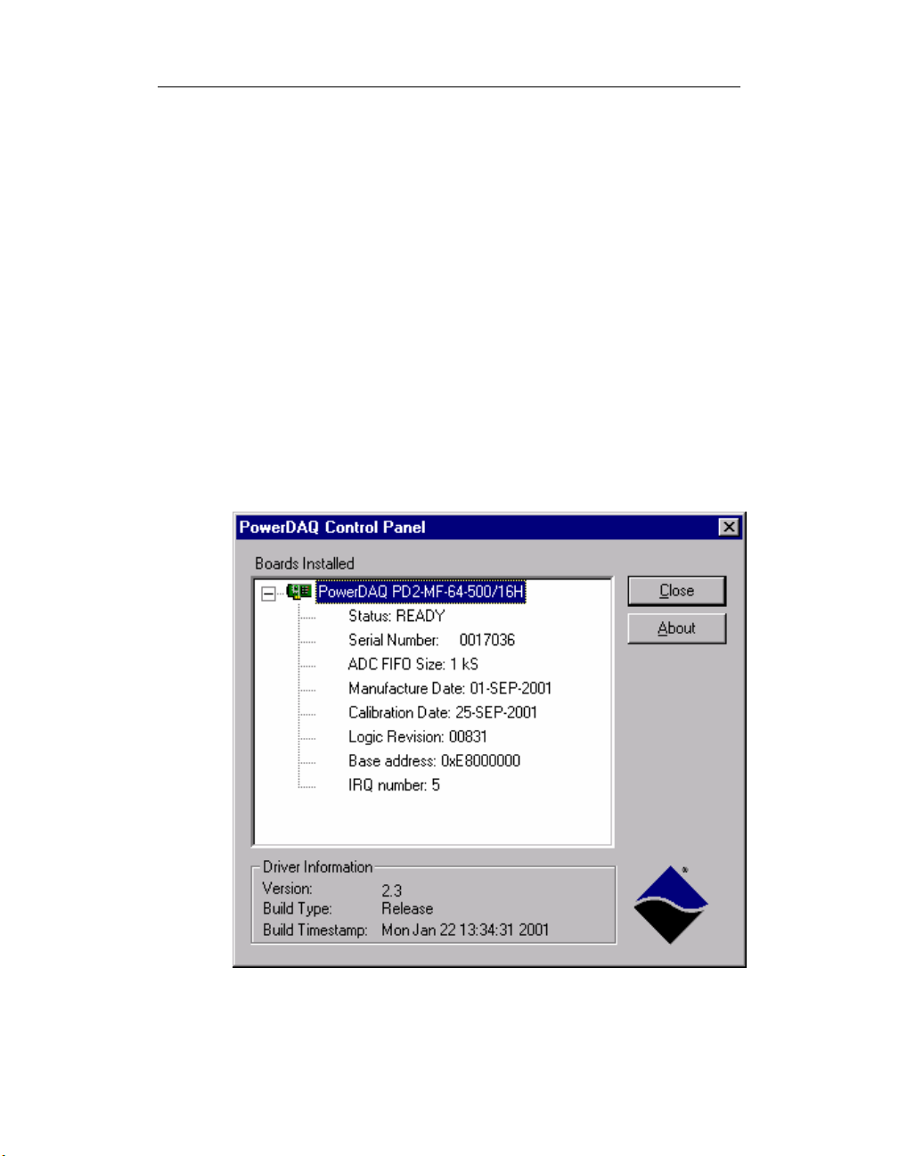
• Select Programs ! PowerDAQ !
the Start menu. If the Control Panel applet is displayed
and correctly identifies your PowerDAQ board, the
installation is correct.
! Control Panel: from
!!
Figure 1: Control Panel Application
1
Page 28
Chapter 2: Installation and Configuration
6
Configuring the PowerDAQ Board
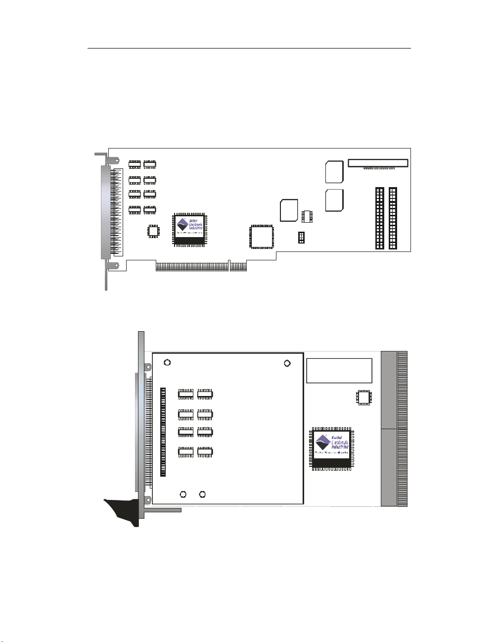
1
J1 Con nector
Pow erDAQ II MF b oard
Inp ut Multi p le xors
DSP
PowerDAQ
PCI Bu s
Control
Logic
Boot
ROM
1
J6 Connector
Logic
FIFO
Onboard
FIFO
Onboard
Low Noise DC-DC
1
1
J4 C onnector
J2 Connector
Figure 2: PD2- Board connector layout
PDXI-MF board
1
J1 C onn e ct o r
J2 Connector
Input M ultiple xors
Low N oise DC-DC
PXI
DSP
Po w er D AQ
CompactPCI Bus
Figure 3: PDXI-MF Board connector layout
1
Page 29
Chapter 2: Installation and Configuration
7
1
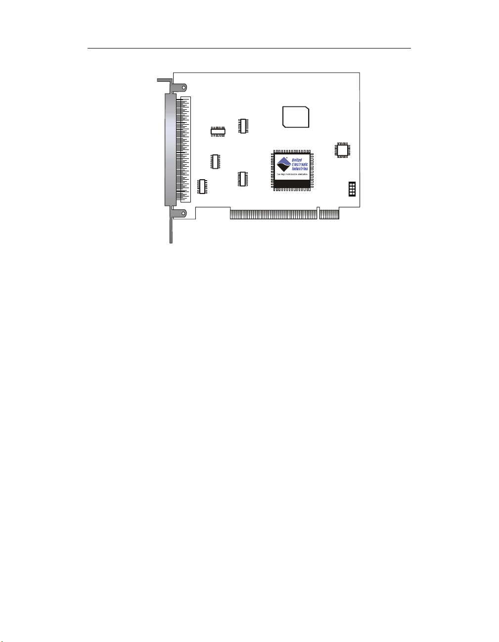
J1 Connector
PowerDAQ PDL-MF board
Boot
ROM
DSP
PowerDAQ
PCI Bus
Figure 4: PDL-MF- Board connector layout
Input Modes:
The analog input section multiplexes the active input channels (64/16
single-ended or 32/8)differential) to a single 12- or 16-bit successive
approximation analog-to-digital converter (ADC).
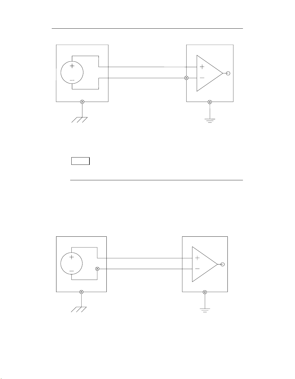
Single-Ended:
PowerDAQ boards can be configured to operate with either a singleended or differential input. Single-ended inputs allow up to 64 channels
and share a common return path connected to analog ground (AGND).
1
Page 30
Chapter 2: Installation and Configuration
Ain
V1
Aout
Agnd
Figure 5: Single-ended Inputs and pseudo-differential
inputs
Note Unused channels should be shorted to ground using 0-
to 1-KΩ resistor. In pseudo-differential mode ground reference
level is taken from remote system.
Differential Inputs:
Differential inputs allow up to 32 channels. Each differential channel
uses two analog channels — one analog channel connects to the positive
input of the programmable gain amplifier, and the other to the
negative.
Ain (+)
V1
Ain (RETURN)
AGND
Figure 6: Differential Inputs
18
Page 31

Chapter 2: Installation and Configuration
Note Positive and negative differential inputs should not be
driven by voltages more then AGND ±14V.
When wiring applications to your PowerDAQ board, consider the
following:
• When working in an environment with electrical noise or
when using gains, use differential input.
• When working in an environment with electrical noise,
use individually shielded twisted-pair wiring.
• Physically separate wiring paths or conduits carrying
power lines and signal lines.
• Signal cables should never be put in the same wiring
harness as high-current or high-voltage cables. Avoid
routing signal and power cables together in parallel paths
unless a reasonable distance separates the paths —
reasonable
power signals and the amount of shielding.
• Signal lines near devices that create high levels of
electrical noise should be run through a metal cable
trough above or below the work area.
• Power lines, poorly designed video monitors and
switching power supplies, solenoids, electric arcs from
breakers or welders, and unshielded signal cables can
affect the accuracy of your measurements.
being determined by the strength of the
Installing Multiple Boards (PD-CBL-SYNC):
You can install multiple PowerDAQ boards in one PC. The internal J6
synchronization header will allow a master/slave configuration to be
setup. A special PowerDAQ cable (PD-CBL-SYNC): will allow you to
connect up to four boards in one PC. Synchronization cables for more
than four boards are available from your distributor or the factory.
19
Page 32

Chapter 2: Installation and Configuration
Note PXI boards are synchronized via PXI interface using the
PXI Configurator program.
Figure 7: PDXI Configurator
PDL-MF board is synchronized via connections on a screwterminal panel.
Note When using more than 4 PCI slots (standard PC), you
will need a PCI bridge chip to support additional PCI slots. These
bridge chips reduce the PCI bus throughput and will reduce your
maximum sampling speed.
Base address, DMA, Interrupt settings
The PowerDAQ boards are configured automatically by the PCI bus on
power up. You do not have to set any base address, DMA channels or
interrupt levels. In case of the performance problems try for more
PowerDAQ boards and mass-storage/video/network/USB devices for
different IRQs.
20
Page 33

Chapter 2: Installation and Configuration
Test Program:
After you have wired an application to your PowerDAQ board, you
should run the Simple Test program:
1. Select Programs " PowerDAQ " Simple Test : from
the Start menu. The Simple Test dialog box is displayed.
Figure 8: Simple Test Application
2. Use the Analog In, Analog Out, Digital In, Digital Out,
and Counters tabs to observe your application running
on the board.
Connectors for PD2/PDXI
PowerDAQ multifunction boards have four connectors:
• 96-contact pin-less main connector (J1)
Manufactured by: Fujitsu: PN# FCN-245P096-G/U (Male)
http://www.fta.fujitsu.com/
21
Page 34

Chapter 2: Installation and Configuration
2
• 36-pin internal digital connector (J2)
Manufactured by: Thomas and Betts PN# 609-3627
(Male)
http://www.thomasandbetts.com/
• 36-pin internal digital connector (J4)
Manufactured by: Thomas and Betts PN# 609-3627
(Male)
http://www.thomasandbetts.com/
• 8-pin internal digital clock-signal connector (J6)
Manufactured by: Adam Tech PN# PH2-08-TA-SMT
http://www.adam-tech.com/
Connector Pin Assignments for J1
Figure 9: Fujitsu Connector Layout
2
Page 35

Chapter 2: Installation and Configuration
J1 Connector (Single-Ended Mode)
49
AGND
AGND
AGND
AGND
DGND
AGND
AIN55
AIN53
AIN51
AIN49
AGND
AIN38
AIN36
AIN34
AIN33
AIN23
AIN21
AGND
AIN18
AIN16
AIN6
AIN5
AIN3
AIN1
DSP Trigger Input/AO External Clock
*ADC Conversion Start Out/ Pacer clock out
ADC Channel List Start Input / Burst Clock
AGND
N/C
AGND
AIN62
AIN60
AIN59
AIN57
AIN47
AGND
AIN44
AIN42
AIN40
AGND
AIN29
AIN27
AIN25
AIN24
AIN14
AIN12
AGND
AIN9
Table 8: J1 Connector (Single-Ended Mode)
AGND
1
50
AOUT0
2
351
AGND
452
AOUT1
553
AGND
AGND
654
755
AIN54
AIN52
856
57
AIN50
AIN48
10 58
AIN39
11 59
AIN37
12 60
AIN35
13 61
AGND
62
AIN32
15 63
AIN22
16 64
AIN20
17 65
AIN19
18 66
AIN17
19 67
AIN7
20 68
AGND
21 69
AIN4
22 70
AIN2
23 71
AIN0
24 72
AGND
25 73
26 74
+5V (100 mA max)
ADC Conversion Start Input / Pacer clock
27 75
28 76
AGND
N/C
29 77
30 78
AIN63
AIN61
31 79
32 80
AGND
AIN58
33 81
34 82
AIN56
AIN46
35 83
36 84
AIN45
37 85
AIN43
38 86
AIN41
39 87
AIN31
40 88
AIN30
41 89
AIN28
42 90
AIN26
43 91
AGND
44 92
AIN15
45 93
AIN13
46 94
AIN11
47 95
AIN10
48
96
AIN8
* Disconnected by default, consult factory if you need this clock on J1
connector.
23
Page 36

Chapter 2: Installation and Configuration
4
J1 Connector (Differential Input Mode)
AGND
AGND
AGND
AGND
DGND
AGND
AIN55
AIN53
AIN51
AIN49
AGND
AIN38
AIN36
AIN34
AIN33
AIN23
AIN21
AGND
AIN18
AIN16
AIN6
AIN5
AIN3
AIN1
AGND
DSP Trigger Input/AO External Clock
ADC Conversion Start Out/ Pacer clock out
N/C
AGND
ADC Channel List Start Input / Burst Clock
AIN54 Return
AIN52 Return
AIN51 Return
AIN49 Return
AIN39 Return
AGND
AIN36 Return
AIN34 Return
AIN32 Return
AGND
AIN21 Return
AIN19 Return
AIN17 Return
AIN16 Return
AIN6 Return
AIN4 Return
AGND
AIN1 Return
49
AGND
1
50
AOUT0
2
351
AGND
452
AOUT1
553
AGND
AGND
654
755
AIN54
AIN52
856
57
AIN50
AIN48
10 58
AIN39
11 59
AIN37
12 60
AIN35
13 61
AGND
62
AIN32
15 63
AIN22
16 64
AIN20
17 65
AIN19
18 66
AIN17
19 67
AIN7
20 68
AGND
21 69
AIN4
22 70
AIN2
23 71
AIN0
24 72
AGND
25 73
26 74
+5V (100 mA max)
ADC Conversion Start Input / Pacer clock
27 75
28 76
AGND
N/C
29 77
30 78
AIN55 Return
AIN53 Return
31 79
32 80
AGND
AIN50 Return
33 81
34 82
AIN48 Return
AIN38 Return
35 83
36 84
AIN37 Return
37 85
AIN35 Return
38 86
AIN33 Return
39 87
AIN23 Return
40 88
AIN22 Return
41 89
AIN20 Return
42 90
AIN18 Return
43 91
AGND
44 92
AIN7 Return
45 93
AIN5 return
46 94
AIN3 Return
47 95
AIN2 Return
48
96
AIN0 Return
Table 9: J1 Connector (Differential Input Mode)
2
Page 37

Chapter 2: Installation and Configuration
5
Connector Pin Assignments for J2
The J2 digital internal connector contains eight digital input and eight
digital output lines.
CTR0-IN
CTR0-OUT
CTR0-GATE
CTR1-IN
CTR1-OUT
DIN0
DIN1
DIN2
DIN3
DIN4
DIN5
DIN6
DIN7
Burst Clock / ADC Channel List Start Input
Pacer Clock / ADC Conversion Start Input
DGND
Burst Clock /ADC Channel List Start Output
Table 10: Connector Pin Assignments for J2
CTR2-IN
12
CTR2-OUT
34
CTR2-GATE
56
CTR1-GATE
78
+5V (100 mA max)
910
DGND
11 12
DOUT0
13 14
16
DOUT1
17 18
DOUT2
19 20
DOUT3
21 22
DOUT4
23 24
DOUT5
26
DOUT6
27 28
DOUT7
DGND
29 30
ADC Conversion Start Output / Pacer Clock Output
31 32
DGND
33 34
35 36
NC
2
Page 38

Chapter 2: Installation and Configuration
6
Connector Pin Assignments for J4
The J4 Connector contains eight digital input and eight digital output
lines.
DIN8
DIN9
12
DGND
34
DGND
56
DGND
78
DGND
910
+5V (100 mA max)
11 12
DGND
13 14
DOUT8
16
DOUT9
17 18
DOUT10
19 20
DOUT11
21 22
DOUT12
23 24
DOUT13
26
DOUT14
27 28
DOUT15
29 30
DGND
DGND
31 32
33 34
DGND
35 36
DGND
DGND
DGND
DGND
DGND
DGND
DIN10
DIN11
DIN12
DIN13
DIN14
DIN15
DGND
DGND
DGND
DGND
DGND
Table 11: Connector Pin Assignments for J4
2
Page 39

Chapter 2: Installation and Configuration
7
Connector Pin Assignments for J6
The J6 Interboard Synchronization Connector contains two pairs of
clock signal lines:
• The ADC Clock (also known as the conversion clock.
• The Channel List Clock (also known as the scan clock or
burst clock).
CV_START_OUT
CL_START_OUT
CV_START_IN
CL_START_IN
12
34
56
78
DGND
DGND
DGND
DGND
Table 12: Connector Pin Assignment for J6
Connectors for PDL-MF
PowerDAQ multifunction boards have one connector:
• 100-way connector (J1)
Manufactured by: Fujitsu : PN# FCN-245P096-G/U
(Male)
http://www.fta.fujitsu.com/
2
Page 40

Chapter 2: Installation and Configuration
Connector Pin Assignments for PDL-MF J1
TMR0
DGND
TMR1
DGND
TMR2
DGND
DOUT22
DOUT20
DOUT18
DOUT16
DOUT14
DOUT12
DOUT10
DOUT8
+5VPJ2
DOUT6
DOUT4
DOUT2
DOUT0
DIN22
DIN20
DIN18
DIN16
DGND
DIN14
DIN12
DIN10
DIN 8
DIN 6
DIN 4
DI N 2
DIN 0
AGND
AOUT1
EXT_GND
AIN 7
AGND
AIN 6
AGND
AI N 5
AGND
AIN 4
AGND
AI N 3
AGND
AI N 2
AGND
AIN 1
AGND
AIN 0
EXT_C LK
1
51
2
DGND
52
IRQC
3
53
4
DGND
54
EXT_TRIG
55
5
DGND
56
6
DOUT 23
7
57
DOUT 21
8
58
DOUT 19
9
59
DOUT 17
10
60
DOUT 15
11
61
DOUT 13
12
62
DOUT 11
63
13
DOUT 9
14
64
DGND
65
15
66
DOUT 7
16
DOUT 5
17
67
DOUT 3
18
68
DOUT 1
19
69
DIN2 3
20
70
DIN2 1
21
71
DIN19
22
72
23
DIN17
73
DGND
74
24
DIN15
25
75
DIN13
26
76
DIN11
77
27
DIN9
28
78
DIN7
79
29
DIN5
30
80
DIN3
31
81
DIN1
32
82
AGND
33
83
AOUT 0
34
84
AGND
35
85
AIN15
36
86
37
AGND
87
AIN14
88
38
AGND
39
89
AIN13
40
90
AGND
91
41
AIN12
42
92
AGND
93
43
94
AIN11
44
AGND
45
95
AIN10
96
46
AGND
47
97
AIN9
48
98
AGND
99
49
AIN8
50
10 0
Table 13: Connector Pin Assignments for PDL-MF J1
28
Page 41

Chapter 2: Installation and Configuration
Connector Pin Assignments for PDXI J2
DOUT11
DIN13
DOUT12
DIN14
DOUT13
DIN15
DOUT14
DOUT15
DGND
DGND
DGND
DGND
DGND
DGND
DGND
DGND
DGND
DGND
DGND
DGND
DGND
DGND
DGND
DGND
DGND
DGND
DGND
DGND
DGND
DGND
DGND
DGND
DGND
UCT0_CLK_IN
UCT2_CLK_IN
UCT0_OUT
UCT2_OUT
UCT0_GATE
UCT2_GATE
UCT1_CLK_IN
DIN12
2
1
DOUT10
3
4
DIN11
5
6
DOUT9
7
8
DIN10
9
10
DOUT8
11
12
DIN9
13
14
DGND
15
16
DIN8
18
+5VPJ2
19
20
DGND
21
22
CL_DONE_OUT
23
24
CL_START_OUT_BACK
25
26
DGND
28
DGND
29
30
CL_START_OUT
31
32
CL_START_IN_BACK
33
34
DGND
35
36
TRIG_IN_BACK
37
38
DOUT7
39
40
CL_START_IN_BACK
41
42
DOUT6
43
44
DIN7
45
46
DOUT5
47
48
DIN6
49
50
DOUT4
51
52
DIN5
53
54
DOUT3
55
56
DIN4
57
58
DOUT2
59
60
DIN3
61
62
DOUT1
63
64
DIN2
65
66
DOUT0
67
68
DIN1
69
70
DGND
71
72
DIN0
73
74
+5VPJ2
75
76
UCT1_OUT
77
78
UCT1_GATE
79
80
Table 14: Connector Pin Assignments for PDXI J2
29
Page 42

Chapter 2: Installation and Configuration
0
PXI lines support
Following PXI lines may be used for the synchronization: PXI_TR16 0..7,
PXI_STAR
3
Page 43

3
Architecture
31
Page 44

Chapter 3: Architecture
2
Functional Overview
PowerDAQ PD2-MF/MFS series have very extensive input modes,
clocking and triggering capabilities as well as simultaneous subsystems
operations.
Voltage
Referenc e
Aln Calibrat ion
DACs
Aln Power
Conditioner
(64)
r
o
t
c
e
n
n
o
C
Ext. Aln Con v Clock
O
/
I
Ext. Al n Scan Clock
g
o
l
Ext. Tr igger
a
n
A
Aln C lock Ou t
l
a
n
r
e
t
x
E
Amplifiers
AOut Calibration
16 or 64
Channe l
Analog
Multiplexer
Channe l/
Contr ol
Logic
Analog
Output
DACs
Gain
+
Cust om
PGIA Gain
Amp.
-
Channe l
List
FIFO
DAC0
DAC1
Voltage
Referenc e
12,14,
16-bit
Sampling
A/D
Conver ter
Aln Control
s
s
e
Local Data Bus
r
d
d
A
l
m
e
a
r
n
g
A
n
M
o
a
r
M
A
h
P
R
D
C
k
6
2
1
s
s
e
r
d
d
A
32 Bit PCI Bus
M
p
A
a
R
r
t
M
a
s
t
t
O
a
o
R
D
o
B
k
2
1
k
O
c
F
o
I
l
I
F
C
S
t
S
t
u
E
u
O
O
A
A
Motorola 66MHz DSP 56301
Bus Master PCI Interface
l
o
r
t
n
o
C
Upgradable
1k Sample
ADC
FIFO
UCT Con trol
DIn Control
DOut Control
AIn Clocking & Triggering
v
n
n
a
k
k
o
c
c
c
S
C
o
o
l
l
n
n
C
C
l
l
A
A
a
t
a
D
Figure 10: PowerDAQ PD2 Block diagram
(82C54)
Ext. Aln Con v Clock
Ext. Al n Scan Clock
Ext. Tr igger
Aln C lock Ou t
Interrupt
Config uration
& Calibration
EEPROM
User
Counte r
Timer
Digital
Input
Buffer
Latch
Digital
Output
(Driver)
Clock
Gate
Out
(16)
3
3
4
J
,
2
J
3
s
r
o
t
c
e
n
n
o
C
O
/
I
l
a
t
i
g
i
(16)
D
l
a
n
r
e
t
n
I
n
o
i
t
a
z
i
(4)
n
o
r
h
c
n
y
S
d
r
a
o
b
r
e
t
n
I
3
Page 45

Chapter 3: Architecture
Ext erna l A n al og I/O C onnec t o r
(64)
Mul ti plexer
Ext. Aln Conv Clock
Ext. Aln Scan Clock
Ext. Trig ger
Aln Clock Out
Analog
Outp ut
Amp l if ie r s
AOut Calibration
DA Cs
16 or 64
Ch annel
Analog
Cha nnel/
Gain
Co ntrol
Lo gic
Voltage
Refere nce
+
Custom
PGIA Gain
Amp.
Chann el
Li st
FIF O
DAC0
DAC 1
Voltage
Reference
Aln Calibra tion
DACs
-
Dat a Acqu is ition
ES SI
AOut FIFO
Moto rola 66MHz DSP 56301
Bus Master PCI Interface
Cont rol
Aln Power
Conditioner
12,14,
16-bit
Sam pli ng
A/D
Conver ter
Aln Control
Upgradable
1k Sampl e
ADC
FIF O
UCT Control
PowerDAQ II
Clock ing & Trig gering Lin es
ROM
Clock
Clo ck
Aln Scan
Aln Conv
Bootstrap
Data
DIn Control
DOut Control
Con figuration
& Ca libration
EE PR OM
Control and
Timing Logic
Local Da ta B us
Address
DMA
RAM
6 Channel
12k Program
AOut Clock
32 Bit CompactPCI Bus PXI
12 k D at a RA M
Address
User
Counte r
Timer
(82C5 4)
Ext. Aln Conv Clock
Ext. Aln Scan Clock
Ext. Trigger
Aln Clock Out
Digital
Input
Buffer
Latch
Interrupt
Digit al
Outp ut
(D rive r)
PXI
Contr ol
Logi c
Out
(16)
Clock
Gate
3
3
3
(16)
Internal Digital I/ O Conne ctor J2
Figure 11: PowerDAQ PDXI Block diagram
33
Page 46

Chapter 3: Architecture
4
Remoute Ground
(16)
16 Channel
Analog
Mu ltip lexe r
Channel/
Gain
Co ntrol
Logic
Analog
Out put
Amplifiers
AOut Calibration
DA Cs
Ext. Aln Conv Clock
Ext. Trigger
Aln Clock Out
Voltage
Reference
+
PGIA
Gain
Amp.
-
DSP
Channel List
FIFO
DAC0
DAC1
Volt ag e
Reference
External Analog/Digi tal I/O Conne ctor
Aln Calibration
DA Cs
16-bit
Sam pli ng
A/D
Conve rter
Aln Control
Aln P ow e r
Conditioner
Po w er DAQ I I
Data Acquisition
Control and
Timin g Log ic
Local Da ta Bus
Addr es s
ES SI
DMA
AOut FI FO
6 Chan nel
AOu t Cl o ck
Moto rola 66MH z DSP 56301
Bus Mast er PCI Inte rface
Co ntrol
32 Bit PCI Bus
ROM
RAM
Bootstrap
12k P ro g r am
12k Dat a RA M
Ad d re ss
Dat a
U pgradable
1k S ampl e
ADC
FIFO
Clo ck
Aln Scan
Aln Conv
Cou nter
UCT Control
DIn C on t rol
DOut Control
Clo ck
(3)
DSP
Timer
Figure 12: PowerDAQ PDL-MF Block diagram
(24)
Co n f i g u r a ti o n
& Ca li b r at io n
EE PR OM
Di git al
Input
Buffer
Latch
Digital
Out put
(Driver)
(24)
The heart of the board is the Motorola DSP 56301 running at 66 MHz.
The DSP ensures a highly efficient interface with the PCI bus and
sophisticated control over all board subsystems.
Analog Input subsystem includes:
• The Input multiplexor (MUX) selects which channels to
acquire. The channel list (CL) FIFO controls the input
muxes. PD2-MFS boards have sample-and-hold amplifiers
(SHA) preceding the muxes. SHA amplifiers sample all
3
Page 47

Chapter 3: Architecture
5
input channels simultaneously and then hold the acquired
voltages while the ADC converts channel by channel.
• The Programmable Gain Amplifier (PGA) amplifies an
input signal in order to provide adequate voltage to the
analog-to-digital converter (ADC). The PGA amplification
depends on the board model and can be software
selected {1,2,4,8} or {1,10,100,1000} for MF series boards
and {1,2,5,10} for MFS/PDL-MF boards when the
differential gain (DG) option is installed. Gains are
software selectable on a per-channel basis.
• The A/D FIFOs hold digitized samples until the DSP
transfers them into the host memory, via the PCI bus. The
default A/D FIFO size is 1kS. You can upgrade the A/D
FIFO size to 16kS or 32kS depending on your application.
Larger FIFOs give you smother operations especially at
high acquisition rates and degrade response time in a
case of control loop application.
• The Calibration DACs provide voltages to adjust the
offset and gain settings. All boards are factory calibrated
for each input range and mode specified.
• The Timing, triggering and clocking controls allow you to
select the timebase, clock and triggering sources, “slow
bit” and other options.
• The Interrupt mechanism notifies the DSP about interrupt
conditions
Analog Output subsystem includes:
• DSP based D/A FIFO keeps up to 2kS of digitized
waveform values.
• Digital-to-analog converter (DAC) converts digitized
waveform values into analog output voltages.
• Calibration DACs provide voltages to adjust offset and
gain of analog output.
• Timing, triggering and clocking controls allow you to
select analog output rate and clock source.
• Interrupt mechanism notifies the DSP about interrupt
conditions.
3
Page 48

Chapter 3: Architecture
6
Digital Input/Output subsystem includes
• 16-bit input register to read logical levels on digital input
lines (24-bit on PDL-MF)
• 8-bit Schmidt trigger to catch logic level changes on
digital input lines (not present on PDL-MF)
• 16-bit output register to hold logical levels on digital
output lines, once data has been written (24-bit on PDLMF)
• Interrupt mechanism to notify DSP about interrupt
conditions
User Counter-Timer subsystem includes
• Three 16-bit Intel 82C54 counter timers (fully accessible)
(24-bit DSP 56301 sharable counter/timers on PDL-MF)
• Clock source selection and control logic
• Gate source selection and control logic
• Interrupt mechanism to notify DSP about interrupt
conditions
3
Page 49

Chapter 3: Architecture
7
Analog Input Subsystem
The analog input front-end multiplexes multiplex the first stage of the
input channels (64/16 single-ended or 32/8 differential) into a single,
12, 14 or 16-bit successive approximation ADC. The A/D subsystem also
includes input modes, polarity, gain settings, channel gains, channel
queue, trigger and clocking control.
MF boards have multiplexors located at the signal inputs and can be
switched to select single ended (SE) or differential (DF) mode of
operation (Fig 8). SE/DF mode is selected for all input channels. The
output of the mux signal is fed into a instrumentation amplifier (INA)
and then into a custom programmable gain amplifier (PGA). Channel
numbers along with their gains are stored in the channel list. This allows
you to select different gains on a per-channel basis.
Note Input muxes have high input impedance. It is highly
recommended to ground all unused channels. Use signal sources
with low output impedance (<100 Ohms) to avoid crosstalk;
place a capacitor between signals and ground (SE) or between
signal and return lines on screw terminal (suggested capacitor
values can be 1000pF to 0.047uF depending on your input
frequency).
Note PDL-MF boards also have a jumper-configurable
pseudo-differential mode when ground reference level is taken
from the remote source.
3
Page 50

~
Analog
input 0
…
~
Analog
input N
…
…
MUX A
MUX B
Chapter 3: Architecture
channel and
gain control
INA
SE/DI/PD (PDL-MF only)
switch control signal
PGA
… to range
control,
calibration
circuitry and
ADC
Figure 13: PowerDAQ Multifunction Board front-end
MFS boards have sample and hold amplifiers (SHA) located at the
signal inputs. PD2-MFS-DGx options include a INA and PGA in the one
device located on the back side of the board (Fig. 9). SE or DF mode is
selected by grounding negative input of the INA to the boards analog
ground (AGND). Channel numbers along with their gains are stored in
the channel list. This allows you to select different gains on a perchannel basis.
38
Page 51

Chapter 3: Architecture
Analog
input 0
~
INA SHA
PGA
MUX
……
Analog
input N
~
INA SHA
PGA
SE/DF
switch
control
signal
Gain
contro
l
S/H
signal
channel
select
signal
Figure 14: PowerDAQ Sample and Hold Board front-end
The major difference between MF and MFS boards are the SHAs.
‘Sample and Hold’ signal switches SHAs between ‘sampled’ and ‘hold’
states. When the SHA is in a sample state its output repeats its input.
In the hold state, SHAs keep the output voltage at the same level at
time of switching.
… to range
control,
calibration
circuitry
and ADC
39
Page 52

Chapter 3: Architecture
0
Channels
Ch 0
Ch 1
Ch 2
t0 t1t2
Moment of digitizing
Signal level at the moment of
Figure 15: PD2/PDXI Series Acquisition Process
Channels
Ch 0
Ch 1
Ch 2
Hold
t0 t1t2
Moment of digitizing
Signal level
Time
Sampl
Time
Figure 16: PD2/PDXI Acquisition Process
4
Page 53

Chapter 3: Architecture
Figures 10 and 11 show the differences in data acquired using MF and
MFS boards. When a sine wave is applied to the channels 0, 1 and 2.
, t1 and t2 is the time when the channel reading has happened.
t
0
Minimum delay between them is limited by the rated speed of the
board and can be calculated as 1/rate in kS (seconds).
Note PowerDAQ boards acquire channels sequentially at the
rated speed that is referenced as the aggregate rate. When the
channel list contains two channels, per channel rate is a half of
aggregate rate.
Maximum per channel rate can be calculated as:
Aggregate_rate / Number_of_channels (kS/s).
Depending on certain MFS models, maximum per channel rate is slower
because of the hold delay time.
The MF board (fig. 10) acquires input signals with a small delay
between acquisitions. If the input signal frequency is relatively low (510 times lower then acquisition rate), the difference in the acquired
signal level is minimal. Data acquisition is
input signal has a fairly high frequency, sequential acquisition can cause
significant error in the digitized signal levels. MFS board would be
more suitable for such an application.
virtually simultaneous
. If the
The MFS (Fig. 11) board holds the signal at the same level while
digitizing all of the channels in the channel list. There is no difference
in the acquired signal level among the channels. Data acquisition is
simultaneous
have a unique exact timing feature. SHAs have a negative delay. In
other words the signal captured by switching them into the hold mode
is the signal 15ns previously. MFS board control logic delays external
hold signals for the same amount of time. This guarantees that the
board acquires a signal level at the exact time of the external pulse.
require true difference between input channels levels and
working with signals close to nyquist frequency.
regardless of the input signal frequency. The MFS boards
Note Always use PowerDAQ MFS series of board if you
truly
41
Page 54

Chapter 3: Architecture
2
Note Complete timing tables for all PowerDAQ boards are
located Appendix A.
Input Modes
Single Ended
The PowerDAQ boards operate with either a single-ended or a
differential input configuration. Single-ended inputs allow up to 64
channels and share a common low side, which is the analog ground.
Single ended inputs are shown diagrammatically in figure 12.
5 for complete wiring instructions.
Note Unused channels should be shorted to ground using a 0
to 1KOhm resistor.
See Table
+
V1
-
Figure 17: Single-Ended Inputs
4
Ain
Agnd
+
-
Page 55

Chapter 3: Architecture
Differential Inputs
Differential inputs allow up to 32 channels. (Differential inputs use two
analog input channels. One channel connects to the positive input of
the programmable gain amplifier and the other to the negative of the
instrumentation amplifier).
Note Both inputs must remain in AGND ±14V rails; otherwise
input multiplexors lookup may occur.
+
V1
-
Ain (RETURN)
Ain(+)
+
-
Agnd
Figure 18: Differential Inputs
Example: For a 16 channel PowerDAQ board in differential mode,
channels 0 and 8 form the high and low inputs of input channel 0,
channels 1 and 9 that of input channel 1. Differential inputs are shown
diagrammatically below.
See Table 6 for complete wiring instructions.
Note PowerDAQ MFS boards with DG option installed have
the same number of differential and single-ended channels.
43
Page 56

Chapter 3: Architecture
Input Ranges
The PowerDAQ boards have four possible input ranges. These are global
settings.
UNIPOLAR BIPOLAR
0V to +10V - 10V to + 10V
0V to +5V* -5V to +5V
* Not Available on PDL-MF board.
Table 15: Input Range Table
Gain Settings
You can set a gain for each channel prior to acquisition. Depending on
your board, there are three gain ranges.
MF L Gains MF H Gains PDL-MF/
MFS DG-option Gains
1, 10, 100, 1000 1, 2, 4, 8 1, 2, 5, 10
Table 16: Programmable Gains
Note For low-level signals, you need high gains and you
should use a L model. For high level signals, you need a low gain
board and you should use the H model.
44
Page 57

Chapter 3: Architecture
Channel List
The Channel List contains sequences of channels to be acquired and
their per channel gains. This sequence is known as the SCAN. The ADC
Channel List can contain 1 to 256 channel entries (64 entries on PDLMF). Configuration data for each channel will include the channel
selection, gain, and slow bit setting. Each Channel List block written
clears and overwrites the previous settings.
The Slow Bit is a special marker which guaranties longer settling time
for a particular channel. It is very useful when the signal is acquired has
a high (100 or 1000) gain.
The Channel list has the following format:
Bit 8 Bits 7 and 6 Bits 5 to 0
Slow bit Gain Channel to acquire
Table 17: Channel List Format
Gain coding
(bits 7,6)
00 1 1 1
01 10 2 2
10 100 4 5
11 1000 8 10
On PDL-MF channel list may have up to 64 entries.
MF L Gains MF H Gains MFS DG-option
Gains
Table 18: Programmable Gain Codes
45
Page 58

Chapter 3: Architecture
Clocking
The PowerDAQ board has two selectable base frequencies (11 MHz and
33 MHz) to clock acquisition. Lower frequencies are obtained by
dividing the base frequency by a 24-bit number (from 1 to 16M). To
calculate the result frequency use following formula:
Timebase = Base Frequency / (divisor + 1)
Acquisition is clocked by two signals: conversion start (CV Start) and
channel list start (CL Start). There are four selectable sources for these
clocks:
• Software command
• Internal timebase
• External clock
• Continuous clocking (or self-retriggerable clock)
Additionally for internal or external clocks, an active edge (rising or
falling) can be selected.
Note The PowerDAQ board will generate an error condition
each time a clock signal is applied, before the board is ready to
process it. For example, if you clock the board with a clock
frequency higher than the rated aggregate rate, the board
reports a CV/CL start error.
The CV Start clock starts the A/D conversion. The CL Start clock starts
the channel list execution. The CV Start clocks are ignored until the CL
Start pulse is sensed. If any clock is switched to continuous clocking, it
re-triggers itself immediately after board is ready to process it.
Note On the PDL-MF board only one clock may be used at
the time. If CV clock is specified as internal or external, CL clock
must be set to continuous, if CL clock set to internal/external,
CV clock is ignored and board is running A/D on maximum
speed.
46
Page 59

Chapter 3: Architecture
Clock combination Typical use
CL Clock
source
SW Continuous Acquire one set of data points (one
Internal Continuous Continuous acquisition with accurate
External Continuous Continuous acquisition when each run of
Continuous Continuous Performs acquisition at maximum speed
Continuous
or SW
Continuous External MF boards only. Useful when one
Internal Internal Rarely used. MF boards only. Useful with
External External Rarely used. Gives full control of the
SW SW Rarely used. Gives full control of the
CV Clock
source
Internal MF boards only. You can select the
scan). SW clock causes channel list to be
executed once. The board will wait until
next CL clock comes before restarting.
timebase. After each CL Clock pulse, the
channel list is executed at the maximum
acquisition rate. This is the most useful
mode.
the channel list is triggered by the
external signal. This mode is used to
synchronize external events with scans.
possible. Less accurate than using the
timebase.
specific time between conversions. Use
this type of clocking when you want to
increase settling time between
acquisitions especially when your signal
source has high output impedance.
channel is acquired and you want to
start acquisition exactly at the external
pulse edge.
slow scan rates and you need to provide
exact time between conversions.
boards timing to the external device
boards timing to your software
Table 19: Different Clocking Combinations
47
Page 60

Chapter 3: Architecture
Triggering
The Analog input subsystem needs a trigger signal to start and stop
acquisition. The Trigger signal is selectable. It can be either software
command or an external pulse. External trigger is edge-sensitive. You
can select rising or falling edge to be active. If the board is set up to
start on an external trigger, all clocks will be ignored until the pulse
comes. Acquisition continues until the stop trigger comes.
Note If CV Start clock is set to continuous start/stop, the
trigger is guaranteed to start and stop acquisition at the
beginning of channel list. If CV Start is external, it’s up to
external equipment settings.
Note The PDL-MF board provides gated mode on the
external clock, when external trigger line used as a gate for the
internal/external clock. On the MF/MFS boards gated mode may
be implemented using the 8254 counter-timers.
48
Page 61

Start
trigger
edge
Rising Rising
Rising Falling
Falling Falling
Falling Rising
Stop
trigger
edge
External TTL signal
Acquisition started
Acquisition stopped
Chapter 3: Architecture
Table 20: External Trigger Modes
ADC FIFO
The PowerDAQ boards have an on-board FIFO. The FIFO could contain
from 1kS (default) up to 64 kS depending on the FIFO option
purchased.
When the PowerDAQ board acquires data in continuous mode, data is
written into the ADC FIFO. When the FIFO becomes half-full, the DSP
initiates data transfer from the ADC FIFO into the host memory. When
a minimal amount of data is to be transferred to the host memory in
continuous acquisition mode, it is 512 samples for 1kS FIFO, 2048
samples for 4kS FIFO, etc.
49
Page 62

Chapter 3: Architecture
Data format
Data in the data stream has the following format. Each two
consecutive bytes contain a single sample from the A/D converter.
Data is stored repeatedly sample by sample for all channels in the
channel list. (Table 19 shows a PowerDAQ 16-bit board data format.
For PowerDAQ 12-bit boards, only 12 LSBs (Least Significant Bits) are
valid. PowerDAQ II boards automatically place zeroes in any unused bit
locations.)
1st channel 2nd channel … last channel 1st channel …
sample sample sample sample
bit15 bit14 bit13 bit12 bit11 bit10 bit9 bit bit7 bit6 bit5 bit4 bit3 bit2 bit1 bit0
Table 21: Data Format Table for a 16-bit Board
bit15 bit14 bit13 bit12 bit11 bit10 bit9 bit8 bit7 bit6 bit5 bit4 0x0 0x0 0x0 0x0
Table 22: PowerDAQ II 12-bit data format
bit15 bit14 bit13 bit12 bit11 bit10 bit9 bit8 bit7 bit6 bit5 bit4 bit3 bit2 0x0 0x0
Table 23: PowerDAQ II 14-bit data format
bit15 bit14 bit13 bit12 bit11 bit10 bit9 bit8 bit7 bit6 bit5 bit4 bit3 bit2 bit1 bit0
Table 24: PowerDAQ II 16-bit data format
50
Page 63

Chapter 3: Architecture
The following calculations should be performed to convert the raw,
stored hexadecimal data to scaled (Voltage) data:
1. Determine the value of a single bit (“bit weight”) in Volts
depending on the input range.
PowerDAQ II (span)/65535
0 - 5V unipolar (5V span) 0.000076295 Volts/bit
0 - 10V unipolar (10V span) 0.000152590 Volts/bit
+/-5V bipolar (10V span) 0.000152590 Volts/bit
+/-10V bipolar (20V span) 0.000305180 Volts/bit
Table 25: Bit Weight vs. Input Range
2. Determine the “zero offset” which depends on the input
range selected.
5V, 10V unipolar 0
+/-5V biploar -5V
+/-10V biploar -10V
Table 26: Displacement vs. Input Range
3. Perform an arithmetical XOR with 0h8000 for all
PowerDAQ boards
4. Multiply by the “bit weight” from step 1
5. Add the “zero offset” from step 2
6. If a gain other than 1 was used for a selected channel,
divide the value received by the gain factor (Doing this
step last guarantees the maximal data accuracy.)
51
Page 64

Chapter 3: Architecture
7. To convert voltage into analog output value you can use
following formulas:
For all other models
Value = ((HexData XOR 0x8000) * BitWeight +
Displacement) / Gain
52
Page 65

Chapter 3: Architecture
Analog Output Subsystem
Analog output subsystem contains two DACs (Digital to Analog
Converters) and supports the following operating modes:
Single Update
The PowerDAQ PD2-MF(S) boards operate with either a single-update
or streaming (waveform) output configuration. Single-update mode
allows direct write access to the pair of 12-bit DACs. The update
frequency is at least 1 kHz for the single update mode. This single
update speed is dependent on your PC system speed. Since data is
written to the DAC, if holds it indefinetly.
Event-based Waveform
Event-based waveform mode allows continuous waveform generation
and is not limited by the amount of data. The interrupt-based data
requests, from the board, will be received each time the DSP based
FIFO is ½ full. (with 2K samples on-board FIFO, you can load a
maximum of 1024 samples at a time).
Note If the FIFO is empty or the last value is outputted, the
board continues outputting the last value.
Continuous (polled-I/O) Waveform
An alternative continuous waveform mode does not require you to use
the event handling mechanism. Using polled I/O, you initialize the
analog output subsystem, and write data to the output buffer (2048
samples). After the application starts, the buffer is downloaded to the
DSP FIFO and the values are outputted to the DAC’s
53
Page 66

Chapter 3: Architecture
4
Auto-regeneration Waveform (circular
waveform)
Auto-regeneration waveform mode can be used to create fixed length
waveforms (2048 samples maximum) without any host PC intervention
after initialization of the subsystem. An application writes data to the
buffer of the board and each time the end of buffer is reached, it
starts to resend the same buffer again.
Note Revision 3.x of PowerDAQ SDK allows to create
waveforms up to the size of memory available in PC.
Channel List
There is a fixed Channel List for the analog output on the PD2-MF(S)
boards. The channel list always contains channel 0 and 1 and they are
updated simultaneously.
Note The two channels are updated at the same time,
therefore you have to configure both DACs to the same mode
of operation.
Data Format
The analog outputs have a fixed output range of +/- 10V. Data
representation is in straight binary. To convert voltage into binary codes
you can use the following formula.
5
Unused 1
Table 27: Analog Output Data Format
HexValue = ((Voltage + 10V) / 20) * 0xFFF
12-bit output data
for Aout1 1
12-bit output data
for Aout 0
Page 67

Chapter 3: Architecture
5
The two Hex values for Aout channel 0 and 1 respectively can be
combined to write to the analog output as follows:
Value_To_Write = (HexValue1 << 12) OR (HexValue0)
Clocking
The analog output subsystem can be clocked using software command,
internal 11 MHz base frequency or external trigger input line.
In the case where the internal 11MHz timebase is used, calculate the
output rate as follows:
Timebase = 11 MHz / (divisor + 1)
Every time a clock pulse comes, the board reads the next value from
the D/A FIFO and converts it into a voltage and outputs the analog
data on the selected channel.
Triggering
The external trigger line can also be used as an analog output start and
stop trigger. You can select internal clock as the analog output
timebase and use the trigger line to start and stop output.
Additionally you can use the external trigger line to synchronize analog
input with the analog output subsystems.
5
Page 68

Chapter 3: Architecture
6
Digital Input/Output Subsystem
Digital Output subsystem contains one 16-bit (PD2/PDXI-MF/MFS) and
24-bit (PDL-MF) output register. The Digital outputs do not support
clocked output, it can only be used in software-polled mode.
The digital Input subsystem contains one 16-bit (PD2/PDXI-MF/MFS)
and 24-bit (PDL-MF) input register. Digital inputs do not support
clocked input, it can only be used in software-polled mode.
Eight lower lines of the digital input are connected to a latch register.
This register could be programmed to detect rising or/and falling edges
on those digital input lines.
16-bit
Input
Register
8-bit
Edge
Detector
and
Latch
Logic
Input levels
Latch status
Latch config
IRQ
Figure 19: Digital Input Subsystem
5
Page 69

Chapter 3: Architecture
7
Latch configuration is a 16-bit word, two bits for each one of eight
sense inputs.
Bit 7 Bit 6 Bit 5 Bit 4 Bit 3 Bit 2 Bit 1 Bit 0
F R F R F R F R F R F R F R F R
F: 1 in this position, the inputs are sensitive to falling edge
R: 1 in this position, the inputs are sensitive to rising edge
Table 28: Digital Input Configuration Word (PD2/PDXI only)
The Edge Detector and Latch Logic detect configured edges on the
digital input lines. A 8-bit latch register has 1 bit per input line. It is set
to “1” when the configured edge is detected. Additionally, the logic
fires an interrupt to the DSP to inform it when the configured
conditions are met.
If you set up a latch configuration to watch for edges on several lines,
the interrupt fires as soon as any of the selected conditions happen.
However, the interrupt will not be re-fired again until the user
application clears the bit. If a change is detected on another line, the
interrupt will re-fire. To recognize which line caused an interrupt you
have to read the digital input status (i.e. latch register).
5
Page 70

Chapter 3: Architecture
User Counter-Timer Subsystem
PD2/PDXI
User counter-timer is based on the Intel 82C54 16-bit counter-timer
chip. It contains three fully independent counter-timers. It’s fully
dedicated for user applications and it is not used by any of the
PowerDAQ systems. The logic allows you to select the clock and gate
source for each of the three independent counter-timers. The countertimer outputs can generate interrupts to the host PC on change of
their state.
You can feed a clock input from one of the following four sources:
• Software command
• 1-MHz internal timebase
• External clock input line
• UCT0 output line (available for UCT1 and 2)
Gate can be controlled from two sources
• Software command
• External gate input line
Each of the UCT can be used in following modes:
• "Pulse" - generates one pulse with value/frequency length
(Mode 1)
• "Train" - generates pulse train with value/frequency rate.
Pulse length is 1/frequency (Mode 2)
• "Rate" - generates pulse train with value/frequency rate.
Pulse length is 1/2 value/frequency high and 1/2
value/frequency low (Mode 3)
• "Delay" - waits value/frequency time and then generates
one pulse (Mode 5)
See Intel 82C54 datasheet and PowerDAQ SDK examples for
implementation details.
58
Page 71

Chapter 3: Architecture
Special frequency measurement mode is implemented on PD2/PDXI
boards. Using this mode external frequency may be measured in
0..65535 interval with absolute accuracy.
The UCT is extremely useful in combination with the external clock and
trigger lines. Using the UCT you can create very sophisticated
acquisition setups.
PDL-MF
There are three DSP-based 24-bit counter/timers are available on the
PDL-MF board. They are independent from each other and capable to
generate interrupts. Maximum frequency is 16.5 MHz for external and
33 MHz for internal clock. Please refer to Motorola DSP5601 user
manual for the details. (www.mot.com).
Modes:
• timer
• external event counting
• pulse output
• square wave output
• Pulse Width Modulation (PWM) output
• width/period/capture measurement
Note TMR0 is shared with AIn clock, TMR2 is shared with
AOut clock.
59
Page 72

Chapter 3: Architecture
0
6
Page 73

4
PowerDAQ Software
Development Kit
(PD-SDK)
61
Page 74

Chapter 4: PowerDAQ Software (SDK)
2
PowerDAQ Software
PowerDAQ SDK Structure
The installation will create the following directory structure in Program
Files. This assumes you selected the SDK installation (default).
PowerDAQ PowerDAQ root directory
Applications Applications – ready to run
Documentation Documents and manuals
SDK Software developers Kit (SDK)
Examples Examples (including
applications with source code)
C Builder Examples Borland C++ Builder
3.5
Delphi Examples for Borland Delphi
3/4/5
Visual Basic Examples for MS Visual Basic
VB3 Example for 16-bit VB3
VB5 Examples for V5(can use
withVB6)
VB6 Examples for VB6
Visual C Examples for MS
Visual C++ 5/6
Include VB, VC, Delphi API
declarations
16-bit VC files for 16 bit OS
VB3 MS VB3 16-bit files with API
Lib Library .LIB files for VC, Inprise
Borland C++ Builder
Figure 20: PowerDAQ Software Structure
PowerDAQ drivers
Windows 9x operating System
Location: \windows\system directory
Files: pwrdaq95.vxd device driver
Windows NT/2000/XP operating system
6
Page 75

Chapter 4: PowerDAQ Software (SDK)
Location: \winnt\system32\drivers
Files: pwrdaq.sys device driver
PowerDAQ DLLs
The PowerDAQ software includes various DLLs (dynamic linked libraries)
for Windows operating systems. The location of these DLLs is as
follows:
Windows 9x operating System
Location: \windows\system directory
Files: PwrDAQ32.dll 32-bit DLL
PwrDAQ16.dll 16-bit DLL
Windows NT/2000/XP operating system
Location: \winNT\system32
Files: PwrDAQ32.dll 32-bit DLL
PwrDAQ16.dll 16-bit DLL
The DLLs have identical names for Windows 9x and Windows
NT/2000/XP however they are implemented differently. Both of them
support the same API therefore PowerDAQ applications, which do not
use specific Win9x and WinNT/2000/XP functions, would run on both
OS.
PowerDAQ Libraries
PowerDAQ SDK contains libraries for all major software development
tools.
63
Page 76

Chapter 4: PowerDAQ Software (SDK)
4
/lib
pwrdaq32.lib - MSVC/MSVS v.5.x, 6.x
pd32bb.lib - Borland C Builder v.3.0, 4.0
pd16bb.lib - 16-bit Borland compilers
pd16bc45.lib - 16-bit Borland C++ 4.5x
pwrdaq16.lib - 16-bit MSVC 1.5x
PowerDAQ Include Files
/include
pdfw_def.h - firmware constant definition file for C/C++
pdfw_def.pas - firmware constant definition file for Borland Delphi
pdfw_def.bas - firmware constant definition file for Visual Basic
pwrdaq.h - driver constants and definitions file for C/C++
pwrdaq.pas - driver constants and definitions file for Borland Delphi
pwrdaq.bas - driver constants and definitions file for Visual Basic
pwrdaq32.h - API function prototypes and structures file for C
pwrdaq32.hpp - API function prototypes and structures file for C++
pwrdaq32.pas - API function prototypes and structures file for
Borland Delphi
pwrdaq32.bas - API function prototypes and structures file for Visual
Basic
pd_hcaps.h - boards capabilities definition file for C/C++
pd_hcaps.pas - boards capabilities definition file for Borland Delphi
pd_hcaps.bas - boards capabilities definition file for Visual Basic
vbdll.bas - auxiliary functions to access PowerDAQ buffer from
within VB
Aliases.bas - auxiliary functions to access PowerDAQ structures
from within VB
PdApi.bas - module used in SimpleTest VB example
6
Page 77

Chapter 4: PowerDAQ Software (SDK)
5
/include/vb3
pwrdaq16.bas - API function prototypes and structures file for Visual
Basic v.3.0
pdfw_def.bas - firmware constant definition file for Visual Basic v.3.0
pd_hcaps.bas - boards capabilities definition file for Visual Basic v.3.0
daqdefs.bas - event word definition for Visual Basic v.3.0
/include/16-bit
pwrdaq16.h - API function prototypes and structures file for 16-bit
C/C++
pwrdaq.h - driver constants and definitions file for 16-bit C/C++
pdd_vb3.h - auxiliary functions to access PowerDAQ structures
from within VB v.3.0
pd_hcaps.h - boards capabilities definition file for 16-bit C/C++
6
Page 78

Chapter 4: PowerDAQ Software (SDK)
6
Communication between user application and
PowerDAQ PD2/PDXI/PDLboard
PowerDAQ board (using
the PD2 as an example)
DSP
PCI Bus Interface
PowerDAQ driver
PowerDAQ DLL
samples
events
Data Buffer
User Application
Figure 21: Communication between user application and
PowerDAQ board
DSP – Digital Signal Processor controls all on board devices. User
application communicates with the board via the PowerDAQ API
encompassed into the PowerDAQ dynamic-link library (DLL). To inform
application about hardware events, the driver creates Win32 events.
Data is transferred from the board through the PCI bus and stored in
the user-level buffer. The PowerDAQ API includes a set of information
functions which allow user applications to get board-specific
information such as model , serial number, IRQ line, etc.
6
Page 79

Chapter 4: PowerDAQ Software (SDK)
7
Programming subsystems
All PowerDAQ subsystems have two modes of operation:
• Polled
• Event-based
Polled mode is preferred when the application does not need to be
notified about hardware events. Event-based mode allows you to write
truly asynchronous applications.
Opening the subsystems
You have to open the driver, adapter and acquired subsystem before
starting any operation and after completion, release the subsystem ,
close adapter and driver. The manual explains generalized algorithms
and important API calls. For programming details, see “PowerDAQ
Programming Guide.
API calls required for opening subsystems
• PdDriverOpen(…) Opens driver
• _PdAdapterOpen(…) Opens adapter (only one process
can open adapter at a time)
• _PdAcquireSubsystem(…) Acquire named subsystem in use
(if dwAcquire = 1)
• … work with the subsystem, then …
• _PdAcquireSubsystem(…) Releases named
subsystem from
use ( if dwAcquire = 0)
• _PdAdapterClose(…) Closes adapter
• PdDriverClose(…) Closes driver
6
Page 80

Chapter 4: PowerDAQ Software (SDK)
Analog Input Subsystem
There are many ways of working with the analog input subsystem.
Before you start programming your application, consider how you
would like to use the board.
To select the input mode you need to OR your analog input
configuration word with the input mode selection constants.
Input Mode Constant
Single-Ended, 0..5V* 0
Single-Ended, 0..10V AIB_INPRANGE
Single-Ended, -5..+5V AIB_INPTYPE
Single-Ended, -10..+10V AIB_INPTYPE + AIB_INPRANGE
Differential, 0..5V* AIB_INPMODE
Differential, 0..10V AIB_INPMODE + AIB_INPRANGE
Differential, -5..+5V AIB_INPMODE + AIB_INPTYPE
Differential, -10..+10V AIB_INPMODE + AIB_INPTYPE +
AIB_INPRANGE
* Not available in PDL-MF.
68
Page 81

Chapter 4: PowerDAQ Software (SDK)
Method A. Single scan operation
See SDK Examples
vm64.pas, voltmeter.vbp, Vl16.cpp, PDGABoards.cpp
This method is useful when you need to get one set of data points
(one scan). This method allows you to acquire up to 100 scans per
second, depending on the channel list size and maximal board speed.
For example, applications such as a multi-channel voltmeter or
sensor/thermocouple monitor are best suited for this method.
Acquisition can be initiated by software command or external CL Clock
signal. This method does not require buffering because the maximum
number of samples acquired is less then the minimal size of the ADC
FIFO.
Initialization – Method A
Reset the board
Set up configuration
Analog input configuration bits are defined in pdfw_def.h file.
Recommended configuration for Method A is:
SimpleAin.c, simplescan.pas, simplescan.bas,
PdAInReset(…)
_PdAInSetCfg(…)
DwCfg = (AIB_CVSTART0 | AIB_CVSTART1) for software clock
DwCfg = (AIB_CVSTART0 | AIB_CVSTART1 | AIB_CLSTART1) for
external clock
Set up channel list (which can contain one or more scan
sequences)
_PdAInSetChList(…)
Channel list is an array of 32-bit words. See channel list entry format in
“Functional Overview” chapter of this manual
Enable conversions
_PdAInEnableConv(…) with dwEnable = 1
_PdAInSwStartTrig(…) issue start trigger
If software clock is selected, clock the first scan
_PdAInSwClStart(…)
69
Page 82

Chapter 4: PowerDAQ Software (SDK)
Acquisition - call the acquisition sequence using the timer or in a
program loop. Allow all points in the scan to be acquired, then calculate
how much time it takes to digitize the entire channel list. One channel
takes (1 / maximum_board_rate) (s) to be digitized. Do not forget the
“Slow bit” adds additional time and some PowerDAQ MFS models have
small additional “hold delay” time.
Get all sample already acquired
_PdAInGetSamples(…)
If software clock is selected, clock the next scan
_PdAInSwClStart(…)
Note If you are using external pulses to clock the channel list
start, you have to address the situation when the next scan
clock comes; during your _PdAInGetSamples(…) call. This
function will return the number of points that are stored in the
buffer. If the number of scans is equal to the board’s A/D FIFO
size, scan synchronization might be lost. You need to be aware
of these situations in your algorithm. Using
_PdAInEnableConv(…) can enable/disable conversion “on the fly”
and clear A/D FIFO using _PdAInClearData(…).
De-Initialization
Reset the board
_PdAInReset(…)
Note Use averaging if possible. Put several scan sequences
into the channel list and average them to reduce noise and
increase the resolution.
70
Page 83

Chapter 4: PowerDAQ Software (SDK)
Note The PowerDAQ boards have a special “slow bit” in the
channel list. You might want to increase settling time for a
particular channel with the high gain selected or a channel
connected to a high output impedance signal. See your board
specifications to calculate how much “slow bit” affects time
needed to acquire that channel.
71
Page 84

Chapter 4: PowerDAQ Software (SDK)
2
Method B. Burst Buffered Acquisition – One
Shot
See SDK Examples Stream2.c, SimpleExample.vbp
This method is useful when you need to get one-shot data acquisition
with significant delay between acquisition runs. For example if you
need an application like an oscilloscope or FFT , run acquisition one
time, then stop it, analyze data and run it again Method B is for you.
The size of the acquired data will required buffered A/D FIFO reads.
This method requires initializing and using the PowerDAQ buffering
mechanism. See Appendix C to learn more about the PowerDAQ
buffering mechanism.
Method B uses asynchronous notification from the driver via Win32
events. This means that you should program the board for
asynchronous operation and use Win32 function such as
WaitForSingleObject(…) to wait until the driver notifies that data is
acquired.
Initialization
• Reset the board
# _PdAInReset(…)
• Allocate and register buffer with the board
# _PdAllocateBuffer(…)
Use as big a buffer as you need. Buffer size is limited by
the amount of memory installed on your PC. Buffer should
contain at least two frames. The PowerDAQ API allocates
buffers for you.
# _PdRegisterBuffer(…)
Register the buffer with the AnalogIn subsystem. Use
dwWrapAround = FALSE for single-run operation.
• Set up analog input configuration and events you want to
be notified of:
Analog input configuration bits as defined in the file
pdfw_def.h. Recommended configuration for Method B is:
dwCfg = (AIB_CVSTART0 | AIB_CVSTART1 |
AIB_CLSTART0) for internal clock
7
Page 85

Chapter 4: PowerDAQ Software (SDK)
dwCfg = (AIB_CVSTART0 | AIB_CVSTART1 |
AIB_CLSTART1) for external clock
Add AIB_INTCLSBASE constant to select 33 MHz base
frequency instead of 11 MHz.
Analog input event bits are defined in the file pwrdaq.h.
Recommended event notification method:
dwEvents = eFrameDone + eBufferDone + eBufferError +
eStopped
Your application will be notified when at least one frame is
done. The buffer will be filled with data or buffer error, if
an error occurs. The most common reason for buffer errors
is heavily loading from other applications running on the PC
during acquisition and the interrupt was not serviced in
time. Consider using the A/D FIFO upgrades to improve
system performance. (PD-16KFIFO or PD-32KFIFO).
Initiate asynchronous operation
# _PdAsyncInit(…)
Use selected input configuration and events. Provide
dwAInClClkDiv to set up the desired scan rate. Fill and pass
channel list as it was explained in Method A. Make sure
that aggregate rate set up (scan rate * number of
channels) is lower or equal to the maximum board rate.
• Set up event notification
# _PdAInSetPrivateEvent(…)
The API will create Win32 events for you and return a valid
event handle.
• Start asynchronous operation
# _PdAInAsyncStart(…)
This call starts asynchronous operation.
Acquisition
• Wait for event notification
# WaitForSingleObject(hEventObject, Timeout)
This function puts your program into a sleep mode and
gives processor time to other processes. It is activated when
the board signals an event or the timeout period has
expired. The timeout period should be long enough to fill
73
Page 86

Chapter 4: PowerDAQ Software (SDK)
your buffer with samples. When it returns event from the
board you have to check what caused it
• Check events
# _PdGetUserEvents(…)
This function returns events for the subsystem specified
(AnalogIn). Your code should analyze them and make a
decision based on the result.
An Event word could contain following flags:
eFrameDone – get a frame of data
eBufferDone + eStopped – acquisition is completed. All
data is stored in the buffer. Data is available for analysis.
eBufferError – data integrity was compromised because of
lack of performance or system latency while serving
interrupts (see note about interrupts). On board A/D FIFO
overflows. If error persists check interrupt settings and/or
purchase bigger A/D FIFO option.
• Reset events
# _PdSetUserEvents(…)
Call this function to notify the driver that events are
processed.
Restart
• Stop asynchronous operation
# _PdAInAsyncStop(…)
# _PdAInAsyncTerm(…)
This call stops asynchronous operation. You need to call
these functions before you call _PdAInAsyncInit(…)and
_PdAInAsyncStart(…).You can start and restart acquisition
as many times as your application needs. Each time you
restart acquisition, board overwrites data in the buffer with
a new one.
De-Initialization
• Stop asynchronous operation
# _PdAInAsyncStop(…)
# _PdAInAsyncTerm(…)
• Release event object handle
# _PdAInClearPrivateEvent(…)
• Unregister and deallocate buffer
74
Page 87

Chapter 4: PowerDAQ Software (SDK)
# _PdUnregisterBuffer(…)
# _PdFreeBuffer(…)
Note External trigger. If you want your acquisition process
to be started (or stopped) by an external pulse, connect your
trigger source to the external trigger line and setup your analog
input configuration word (dwAInCfg) with trigger settings as
stated below.
75
Page 88

Chapter 4: PowerDAQ Software (SDK)
Trigger type Configuration
Start trigger rising edge AIB_STARTTRIG0
Start trigger falling edge AIB_STARTTRIG0 + AIB_STARTTRIG1
Stop trigger rising edge AIB_STOPTRIG0
Stop trigger falling edge AIB_ STOPTRIG0+ AIB_STOPTRIG1
Table 29: Setting up External Trigger
When the board is clocked from the low frequency
TIP
internal timebase or external clock you might not get an
immediate response because the board transfers data
into the host memory only when the A/D FIFO becomes
half-full. For example, if your board’s FIFO size is 1kS,
acquisition rate is 100Hz and you put one channel into
the channel list, the board notifies the driver (and
application) only after 5 seconds of acquisition no
matter how small your frame is. If you clock your board
externally you will not get any response from the board
until the board will get enough pulses to get half-a-FIFO
of samples. However, you can use
_PdImmediateUpdate(…) function on a timer loop to
force data from the A/D FIFO into the host buffer. Do
not call this function too frequently because it can
degrade system performance.
76
Page 89

Chapter 4: PowerDAQ Software (SDK)
Method C. Continuous Acquisition using ACB
See SDK Examples Stream2.c
Method C uses the PowerDAQ Advanced Circular Buffer mechanism.
Acquisition runs continuously and each time an event occurs, the
application takes control. You can create separate threads in your
application to run the acquisition process.
Analog input configuration is very similar to Method B, however the
buffer is setup is a different way:
Set up the buffers
• Allocate and register the buffer with the board
# _PdAllocateBuffer(…)
Use as big a buffer as you need. The buffer size is limited
by the amount of memory installed on your PC. You can
specify from two to N frames to use. Frame size (in scans)
notifies the driver when the application wants to receive
eFrameDone events. In the case of two frames per buffer
we’re dealing with the classic double-buffering mechanism.
The larger number of frames makes the operations elastic
and decreases probability of buffer overflow.
• _PdRegisterBuffer(…)
Set dwWrapAround = AIB_BUFFERWRAPPED to use
the circular buffer. The circular buffer mechanism is
explained in Appendix C.
Applications should process events in a different way. Each time it
detects eFrameDone events it means that one or more frames were
filled with data.
Acquisition
• Wait for event notification
77
Page 90

Chapter 4: PowerDAQ Software (SDK)
# WaitForSingleObject(hEventObject, Timeout)
This function puts your program into a sleep mode and
gives processor time to other processes. It is activated when
the board signals an event or the timeout period has
expired. The timeout period should be long enough to fill
your buffer with samples. When it returns event from the
board you have to check what caused it
• Check events
# _PdGetUserEvents(…)
This function returns events for the subsystem specified
(AnalogIn). Your code should analyze them and make a
decision based on the result.
An Event word could contain following flags:
eFrameDone – get a frame of data
eBufferDone + eStopped – acquisition is completed. All
data is stored in the buffer. Data is available for analysis.
eBufferDone + eBufferWrapped – data has reached the
end of the buffer. The next frame to fill is located at the
start of the buffer.
eStopped – acquisition is stopped. The reason could be a
trigger pulse on external trigger line, software command or
buffer error. Also, if the application does not take data
fast enough from the buffer and there is no room to place
new incoming data. Check other bits to find what caused
acquisition to stop.
eBufferError – data integrity was compromised because of
lack of performance or system latency while serving
interrupts (see note about interrupts).
eStopTrig – acquisition was stopped because of the stop
trigger pulse or software command
• Get data
# _PdAInGetScans(…)
Retrieves information about position of unread frame in
the buffer
available for the application (NumValidScans). If the
boundary of buffer has been crossed and data fills the
buffer from the beginning, the eFrameDone event will
come twice. The first time it comes to let the user
application retrieve data from the point of the last retrieval
to the end of the buffer and second time from the
beginning of the buffer to the latest complete frame.
n scans
(ScanIndex) and the number of scans
During any _PdAInGetScans(…) call, the application gets the
78
Page 91

Chapter 4: PowerDAQ Software (SDK)
data in a one piece.
application to take care about data wrap around situations.
_PdAInGetScans(…) has a side effect. When it’s called it
marks frames it returns as “read”. This means that these
frames can be reused for new data.
• Reset events
# _PdSetUserEvents(…)
Call this function to tell the driver that events are
processed.
This eliminates need of the user
• Perform your application specific tasks. At this point you
can do whatever you want with the data. Make sure that
your procedure is short enough to process everything you
need before the next eFrameDone event. Otherwise the
buffer can overflows and the driver can stop acquisition.
79
Page 92

Chapter 4: PowerDAQ Software (SDK)
0
How to find optimal frame size for data acquisition?
TIP
The following should be taken into account when
selecting the frame size. Events consume host CPU and
on-board DSP time and a small frame decreases overall
system performance, on the other hand, larger frames
decrease event rates and you might need faster
response especially in control-loop applications.
Performance-wise we recommend selecting frame sizes
to receive 4 to 10 events/second. For example, if you
have four channels in the channel list and the
acquisition rate is 100k scans/s, the recommended
frame size is from 10000 to 25000 scans.
How to determine optimal buffer sizes and number
TIP
of frames? Normally four frames in a buffer are
enough to obtain smooth operation. Four frames give
enough time to avoid buffer overflow if the OS delays
in responding. The buffer should be big enough to
accommodate from 0.33 to 1 second of streaming data.
Note
Analog trigger, pre- and post- triggers. This is
implemented in your user application or application yourself or
using 3rd party software such as LabVIEW, DASYLab, DIADem,
TestPoint or HP VEE. Analog trigger support has been
implemented in these drivers.
Reading thermocouples and other slow-speed
TIP
processes. There’re two ways of reading slow-speed
processes. Method A is better when your application
does not require a precise timebase and it needs 10 data
points per second or less. Method C is better for rates
over 10 data points per second. If you need faster
update rates you can either use
_PdImmediateUpdate(…)call on a timer loop or let the
driver do it by calling _PdAInEnableTimer(…). Actually,
both functions force the board to move all samples
from A/D FIFO to the buffer. The difference is that
_PdAInEnableTimer(…) starts/stops the built-in timer in
the driver.
8
Page 93

Chapter 4: PowerDAQ Software (SDK)
Method D. Retrieving ‘always-fresh’ data using
ACB recycled mode
See SDK Examples Stream2.c
Another very useful feature introduced by the PowerDAQ API’s ACB is
recycled buffering mode. It allows frames to be overwritten with new
data without reading it. For example, you can run acquisition in
continuous mode as it was explained in Method C. If at one time your
application needs much longer time to process data then there is time
to fill the frame, the driver continues acquisition. All frames that were
not retrieved will be overwritten with the new data. When your
application will receive next event, the eFrameRecycled flag will be set.
To switch your buffer into this mode, setup buffer as follows:
• _PdRegisterBuffer(…)
Set dwWrapAround = AIB_BUFFERRECYCLED to use
recycled mode of the circular buffer. This mode is
explained in Appendix C.
One of the obvious reasons to use this mode is in situations when you
cannot predict the exact time needed to process the data. For example,
your control application monitors input data streams, at some point it
needs to perform exhaustive calculations and change equipment
settings. Instead of stopping and restarting the process it leaves the
acquisition running. After processing is completed it keeps up with the
latest data received.
Multithreaded applications with data visualization.
TIP
One of the best ways of writing data acquisition
applications with visualization is to run data operation
and visualization in separate threads.
81
Page 94

Chapter 4: PowerDAQ Software (SDK)
2
Method F. Multi-board operations. Stream to
disk applications
See SDK Examples stream4.c, SingleBoardStreamBasic.vbp
A special cable to synchronize data acquisition from several boards is
required ( PD-CBL-SYNC4 See Appendix) . This cable has one master
connector and three slaves. (Custom versions of this cable are available
for more than 4 boards in one system). It connects the CL and CV clock
outputs from master board to CL and CV clock inputs of the slave
boards. For the PDXI boards all synchronization settings must be done
via PDXI Configurator. To synchronize multi-board acquisition you
should program the master board CL (or CV) clock to use internal,
external or SW clocking and the slave boards to use external CL (or CV
clock). Any of the Methods A thru D can be used.
The best way to set up multi-boards operation is to launch separate
execution threads for each board. Start the slave boards threads first
and then the master board thread.
8
Page 95

Chapter 4: PowerDAQ Software (SDK)
Method G. Combining Analog and Digital
subsystems
See SDK Examples
The tricky part of combining digital and analog operations is the event
handling. The PowerDAQ API has two sets of function to solve this.
The first way is to set up all subsystem operations in a one thread and
create an event using _PdSetPrivateEvent(…). This function creates a
single event that is set when any subsystem needs attention. Note that
each active subsystem events should be sequentially retrieved and
processed. To release a event object use _PdClearPrivateEvent(…).
The second way is to set up each subsystem operation in a separate
thread. You can create separate event objects for each subsystem using
_PdAInSetPrivateEvent(…), _PdAOutSetPrivateEvent(…),,
_PdDInSetPrivateEvent(…),,_PdUctSetPrivateEvent(…),.
SimpleTest.dpr
When one or another subsystem needs an attention, the appropriate
event is set. Subsystem thread wake up on WaitForSingleObject(…),
,Win32 API calls and processes event as described above. To release
event objects use appropriate _PdxxxClearPrivateEvents(…).
Averaging and inertial filters. Use averaging to
TIP
increase resolution and reduce noise. For applications
where the DC value is crucial, consider using an inertial
filter. This filter can be better described as an averaging
window over an array of averages. Each time you
calculate the average value of the frame you put it into
an array of averages replacing the oldest one. Then your
program calculates the average value of the array of
averages and uses it as a final value.
83
Page 96

Chapter 4: PowerDAQ Software (SDK)
4
Method H. Synchronous stimulus/response
operation
This is subset of Method A. Some applications require a analog stimulus
to be applied to a system and a response read. You can do this by
setting the analog input to start the scan from an external clock (CL
Clock line) and the analog output to output the next data point on the
external trigger line pulse. Then connect one of the UCT to start a
countdown from the external trigger line pulse and output to this UCT
to the CL Clock line. When an external trigger pulse is detected, it starts
the countdown and initializes the analog output update. Then the UCT
clocks the CL Clock after the desired delay.
The PowerDAQ board is very flexible and can be configured in many
different ways.
To convert analog input raw values to float voltages use
TIP
the PdAInRawToVolts(…)
Note Shared interrupts and IRQ level. PowerDAQ boards
are designed to share interrupts. We do not recommend
PowerDAQ boards to share interrupts with devices like video and
network cards or hard drives. These devices tie up interrupt lines
extensively and can significantly delay interrupt response from a
data acquisition board. Windows 9x/NT/2000 are not real-time
operating systems however your PowerDAQ data acquisition
board is a real-time application. Many motherboard
manufacturers allow you to set up a IRQ level to a particular PCI
slot. If you do not use serial and/or parallel ports you can
disable them and use IRQs 3, 4, 5, 7 for your data acquisition
boards.
8
Page 97

Chapter 4: PowerDAQ Software (SDK)
5
When starting out, first recognize that a driver for a data
acquisition card differs from one for a printer, CD-ROM or
other peripheral in one fundamental way: real-time operation. A
printer can wait before it gets the next data to print; a CD-ROM
can pause for a short while to let some other activity go on. A
data-acq board, though, typically is collecting data continuously
and can pause only as long as its onboard FIFO can store
intermediate results. If this buffer overflows, incoming data is
lost.
The interrupt can be assigned by the BIOS of your PC and if
allowed, it might be re-assigned during the operation system
boot up process. If you have an Advanced Interrupt Controller
on your motherboard – just enable it in the BIOS – this will
allow you to use more than 16 generic interrupt lines. If not –
use the manual settings to assign the interrupt to the PCI slot
where PowerDAQ board is installed.
Modern motherboards can easily contain four, five or even more
PCI slots plus integrated PCI devices such as network cards
and/or video card. Usually only three of them are independent
and do not share interrupts you’re your video, disk or network
subsystem. Please refer to your motherboard manual to find out
which slots share interrupts and cannot be used for fast data
acquisition.
8
Page 98

Chapter 4: PowerDAQ Software (SDK)
6
Analog Output Subsystem
There are four update modes for the analog output subsystem:
• Polled I/O update mode
• Buffered event-based waveform mode using PCI
interrupts
• Buffered polled-I/O waveform mode
• Auto-retriggerable waveform mode
Method A. Polled I/O update mode
See SDK Examples SimpleAOut.cpp, SimpleTest.vbp
This method allows you to update analog output values immediately
(see Functional Overview for data format).
Initialization
• Reset the board
# _PdAInReset(…)
Output value
• Output analog output value
# _PdAOutPutValue(…)
8
Page 99

Chapter 4: PowerDAQ Software (SDK)
7
Method B. Buffered event-based waveform
mode using PCI interrupts
See SDK Examples AOEvents.c, AEOutBlk.vbp
Buffered event-based waveform mode allows you to generate any
continuous waveforms. When the on-board output FIFO is less than
half full, the board sends an interrupt to the host to request additional
data. You can process analog output events in a separate event handler
or in the common event handler for all subsystems.
Initialization
Reset analog output
# _PdAOutReset(…)
• Set analog output configuration
# _PdAOutSetCfg(…)set dwConfig =
AOB_CVSTART0 to use 11 MHz internal base clock.
• Set timebase
# _PdAOutSetCvClk(…)use the same calculations to
set up the timebase as it was described in the
analog input subsystem
• Set up event object
# _PdAOutSetPrivateEvent(…)
• Enable interrupt
# _PdAdapterEnableInterrupt(…)
• Set events to be notified about
# _PdSetUserEvents(…) set dwEventsNotify =
eFrameDone | eBufferDone | eBufferError |
eStopped. These are all events needed for eventbased waveform mode. Do not forget the
subsystem = AnalogOut
• Write the first block of data
# _PdAOutPutBlock(…)
8
Page 100

Chapter 4: PowerDAQ Software (SDK)
• Enable and start analog output waveform generation
# _PdAOutEnableConv(…) use 1 as dwEnable
# _PdAOutSwStartTrig(…)
Note Use _PdAOutSwStartTrig() to start waveform
generation by software. If you wish to synchronize analog
output signal with external trigger, set appropriate flags in
_PdAOutSetCfg() (flags AOB_STARTTRIG0, AOB_STARTTRIG1,
AOB_STOPTRIG0, AOB_STOPTRIG1 has the same functionality
as for the analog input subsystem).
Wait for events and process them (using
WaitForSingleObject(…) Win32 API call).
Event handler
• Check when event object was set
# _PdGetUserEvents(…)
Look at three events: eFrameDone means that half of the
D/A FIFO is outputted, eBufferDone + eBufferError means
that the entire buffer has been outputted and there is no
more data available.
• Re-Enable Event
# _PdSetUserEvents(…)
• Write the Data
# _PdAOutPutBlock(…)
• Continue waveform generation
# _PdAOutEnableConv(…) use 1 as dwEnable
# _PdAOutSwStartTrig(…)
88
 Loading...