

Page 1

PowerDAQ PD2/PDL/PDXI-DIO
PCI/PXI High-Density Digital I/O Board User Manual
High-Performance Digital I/O boards for PCI/CompactPCI/PXI Bus
Computers
March 2002 Edition
© Copyright 1998-2002 Omega Engineering, Inc. All rights reserved
Page 2

All rights reserved. No part of this publication may be reproduced,
stored in a retrieval system, or transmitted, in any form by any means,
electronic, mechanical, by photocopying, recording, or otherwise
without prior written permission.
Second Edition
Information furnished in this manual is believed to be accurate and
reliable. However, no responsibility is assumed for its use, or for any
infringements of patents or other rights of third parties that may result
from its use.
Contacting Omega Engineering
✉
Address:
OMEGA Engineering, Inc.
One Omega Drive
Stamford, Connecticut 06907-0047
U.S.A.
! Support:
Telephone: 1-800-622-2378
Fax: 1-800-848-4271
"Internet Access:
March 2002 Printing
Support support@omega.com
Web site http://www.omega.com
FTP site ftp://ftp.omega.com
Page 3

Table of Contents
Table of Contents
How to Use This Manual......................................................iii
Introduction........................................................................................... iii
Who Should Read This Book? ...............................................................iii
Organization of This Manual................................................................ iii
Conventions Used in This Manual ........................................................iv
Feedback ................................................................................................v
Introduction ..............................................................................2
About the PowerDAQ DIO board ......................................................... 2
Overview ............................................................................................ 2
Features ............................................................................................. 3
PowerDAQ DIO Applications ................................................................ 5
PowerDAQ DIO Models ........................................................................ 6
Getting Started.......................................................................................7
Installation and Configuration ........................................... 10
Unpacking ............................................................................................ 10
Hardware..............................................................................................10
PCI Installation instructions (PD2-DIO and PDL-DIO)...................... 10
CPCI/PXI Installation instructions (PDXI-DIO) ..................................11
Installing Multiple Boards ................................................................. 12
Software............................................................................................... 12
Windows 9x/NT/2000/XP Installation............................................ 12
Base address, DMA, Interrupt settings ............................................ 13
Diagnostics .......................................................................................14
Accessories ...........................................................................................19
Cables ............................................................................................... 19
Screw Terminal Panels ...................................................................... 21
Complete kits....................................................................................23
Connectors ...........................................................................................23
J1/J2 Connector (PD2-DIO) ..............................................................23
J4/J5 ESSI Connector (PD2-DIO) .................................................... 26
J3 Counter/Timers/IRQx Connector (PD2-DIO) ............................. 26
J1 Connector (PDL/PDXI-DIO)......................................................... 28
J3 Counter/interrupt Connector (PDL/PDXI-DIO) .......................... 28
J4 ESSI Connector (PDL/PDXI-DIO) ................................................ 28
OEM Header Distribution Connector .............................................. 30
Architecture........................................................................... 34
Functional Overview ............................................................................ 36
DSP Processor .................................................................................. 36
PCI/PXI Bus Interface.......................................................................37
Digital Input and Output Subsystem (DIO) .....................................37
Page 4

Table of Contents
ESSI .................................................................................................. 38
DSP Interrupt lines........................................................................... 38
Counter-timers................................................................................. 39
Calibration and startup configuration............................................. 39
PowerDAQ Software........................................................... 42
PowerDAQ DIO board terminology .................................................... 42
Input/Output Mode ............................................................................ 44
Single Update .................................................................................. 44
Timing and Control........................................................................... 51
Enhanced Serial Interfaces (ESSI) ...................................................... 54
Counter/Timer Subsystem .................................................................. 56
High-Speed interrupts ......................................................................... 58
Appendix A: Specifications .................................................60
PowerDAQ DIO specifications: ...........................................................60
IO subsystem ................................................................................... 60
Appendix B: Digital Signal Conditioning..........................63
General Description............................................................................. 63
Technical Specifications ...................................................................... 64
Digital Input Modules...................................................................... 64
Digital Output Modules................................................................... 64
Appendix C: Dimensions......................................................65
Appendix D: Common Questions and Support ..............66
Service and Support .............................................................................67
Technical Support Form................................................................... 68
Appendix E: Warranty..........................................................69
Overview.............................................................................................. 69
Glossary ................................................................................... 71
Page 5

How to Use This Manual
How to Use This Manual
Introduction
This manual describes the PowerDAQ PD2/PDL/PDXI-DIO series Digital
Input/Output boards. These boards are designed for the PCI and
CPCI/PXI buses, 64 and 128 (PD2-only) channel models are available.
Following board models are covered in this manual:
PCI bus
PD2-series
PD2-DIO-64, PD2-DIO-64CT, PD2-DIO64ST
PD2-DIO-128
PDL-series
PDL-DIO-64, PDL-DIO-64CT, PDL-DIO-64ST
CPCI/PXI bus
PDXI-DIO-64, PDXI-DIO-64CT, PDXI-DIO-64ST
Who Should Read This Book?
This manual has been designed to benefit the user of PowerDAQ DIO
boards. To use PowerDAQ DIO, it is assumed that you have basic PC
skills, and that you are familiar with Microsoft Windows
98/Me/NT/2000/XP and/or Linux operating environments.
Organization of This Manual
The PowerDAQ DIO User Manual is organized as follows:
Chapter 1 - Introduction
This chapter gives you an overview of PowerDAQ DIO’s features the
various models available and what you need to get started.
Chapter 2 - Installation and Configuration
This chapter explains how to install and configure your PowerDAQ DIO
board.
Chapter 3 - Architecture
iii
Page 6
How to Use This Manual
This chapter discusses the internal structure and subsystems of your
PowerDAQ DIO board.
Chapter 4 - Interconnections
This chapter describes the I/O connections to your PowerDAQ DIO
board.
Appendix A - Specifications
This chapter lists the PowerDAQ DIO hardware specifications.
Appendix B - Accessories
This appendix lists the PowerDAQ DIO accessories products.
Appendix C - Common Questions and Support
This appendix contains a list of commonly asked questions and their
answers relating to usage and special features of your PowerDAQ DIO
board. Should you require assistance while installing or using
PowerDAQ DIO, support service details are also listed.
Appendix D - Warranty
This appendix contains a detailed explanation of PowerDAQ DIO boards
warranty.
Glossary
The Glossary contains an alphabetical list and description of terms used
in this manual.
Index
The Index alphabetically lists topics covered in this manual.
Conventions Used in This Manual
These are the main conventions used to help you get the most out of
this manual:
Tips are designed to highlight quick ways to get the
TIP
job done, or good ideas you might not discover on
your own.
Note Notes alert you to important information.
iv
Page 7

How to Use This Manual
v
CAUTION!
avoid injury, data loss, or system crash.
Text formatted in bold typeface may also represent type that should
be entered verbatim or a command, as in the following example:
You can instruct users how to run setup using a command such as
setup.exe.
Caution advises you of precautions to take to
Feedback
We are interested in any feedback you might have concerning our
products and manuals. A Reader Evaluation form is available on the last
page of the manual.
Page 8

How to Use This Manual
vi
Page 9

1
Introduction
Page 10

Chapter 1: Introduction
Introduction
This chapter describes the basic features of the PowerDAQ PD2/PDL/PDXI
DIO boards.
About the PowerDAQ DIO board
Thank you for purchasing a PowerDAQ DIO board. The PowerDAQ DIO
board was designed from the ground-up to provide you a best possible
features, reliability and performance available.
The associated PowerDAQ DIO software suite has been written specifically
for these products. Numerous third-party software products are supported
including real-time OS, like QNX and RT-Linux.
Overview
All PowerDAQ Digital IO boards where designed for better
manufacturability and corrected the flaws of 8255 based DIO boards. The
PD2/PDL/PDXI-DIO is feature rich; no longer do you have to design
external circuitry for start-up states, work against problems associated with
the 8255 and relays nor have a separate mechanism for generating
interrupts. Additionally, it features ESD protected I/Os and automatic userdefined values load on power-up, which loads 10mS after the system reset.
The PD2/PDL/PDXI-DIO has it all and more and is the lowest cost of
ownership board on the market.
The PowerDAQ digital input/output boards are configured as 64 or
128 (PD2-only) lines. Board uses 16-bit line drivers, (not 8255 devices)
which allow you to configure the start up states in groups of 16-bit ports.
The on-board DSP/PCI interface allows you to use up to three 24-bit
counter timers, four additional 100nS high speed IRQ lines and two
16.5Mbit/s high speed ESSI ports.
2
Page 11

Chapter 1: Introduction
Features
PowerDAQ DIO boards exist in a three different series:
PD2-DIO, which has 64 and 128 channel boards for the PCI bus and
utilizes 100-way boxed high-density ribbon cable connectors. 64-channel
boards come in a three different versions – static I/O, streaming I/O (-ST)
and counter/timer streaming (-CT). A 128-channel board is available in
static and streaming I/O versions only.
PDL-DIO, 64-channel half-size digital I/O boards which utilizes highdensity 96-way shielded metal pin-less connector. It’s ideal for the noisy
industrial environments and for the space-limited applications.
PDXI-DIO, 64-channel only boards for the cPCI/PXI bus. This is the most
robust and protected version, which shares all cabling and accessories
with PDL-DIO family, but also, implements PXI bus clocking and advanced
triggering support.
The major features of the PowerDAQ PD2-DIO board are:
• 24-bit 80/100 MHz Motorola 56301 DSP (Digital Signal
Processor). DSP runs at 66MHz in order to support 33MHz
32-bit PCI bus
• PCI/cPCI/PXI Bus Host PC Interface (PCI 2.1 Compliant)
• 64/128 lines (5 V/TTL) static I/Os in 16-bit ports;
• High output current drive (-32/64mA)
• Generate interrupts on any line;
• Four Separate High speed IRQ lines (100 ns);
• No legacy '8255' based devices;
• Ideal for solid state relays;
• Per bit user-defined power-up state in groups of 16-bit ports
(High, Low, Tri-stated);
• Two Enhanced Synchronous Serial Interfaces (ESSI);
• Up to three 24-bit counter timers with PWM/measurement
modes available;
• High Speed Digital Streaming to/from Disk (Optional), -ST
and –CT models only;
• Port scan list;
• Multiple boards synchronization via external connections or
PXI bus;
3
Page 12

Chapter 1: Introduction
• Software:
PowerDAQ for Windows 95/98/Me
1
/NT/2000/XP
Linux, RT-Linux and QNX
C, Visual C++, VB, Delphi, C++ Builder
ProffesorDAQ for Excel add-in
Drivers for: LabVIEW®
LabVIEW® for Linux
HP VEE®
LabWindows/CVI®
TestPoint®
DASYLab®
DiaDem®
Note For the full list of specifications,
Specifications.
see Appendix A:
1
PowerDAQ™ SDK version 3.0 and greater will discontinue support of Windows95/98/Me.
Note, that PowerDAQ™ DIO boards are still 95/98/Me compatible and may be used with
PowerDAQ™ 2.x SDK
4
Page 13
Chapter 1: Introduction
PowerDAQ DIO Applications
PowerDAQ DIO family board provides a wide range of powerful features,
which allows using this board in a variety of end-user applications. The
most common applications are:
• Electro-mechanical relays controlled applications
• Solid-state relays applications
• Alarm System sensors
• Digital streaming applications
• Digital motion control and close-loop applications
• Counter/timer streaming
• PWM measurement/generation
• Custom high-speed synchronous serial interface
• Custom DIO/DSP/Counters OEM applications
Note The easiest way to expand the possibilities of PowerDAQ
DIO board is use the PowerDAQ MF, MFS, AO series on
the same PC. The boards are easily synchronized and use
same SDK.
Custom OEM applications that require some hardware or
TIP
software modifications are always welcome and widely
supported by OMEGA ENGINEERING. Please call the
factory to consult with our engineers.
5
Page 14

Chapter 1: Introduction
PowerDAQ DIO Models
PowerDAQ DIO model numbers are derived from the following:
PD[Series]-[Type Of Board]-[Channels][Features]
Series are PD2, PDL and PDXI
Type of the board is DIO
Channels options are 64 and 128 (PD2-DIO only)
Features are CT (event streaming) and ST (digital I/O streaming)
Note Only –ST and –CT boards are suitable for the streamed
I/O operations. Regular DIO boards provide only static
I/O that may be updated only based on the PC clock.
This will work only for the update rates below 1000Hz
under the Windows or 10000Hz under the Linux/QNX
Models Bus DIO Connector DIO Features
PD2-DIO-64
PD2-DIO-64CT
PD2-DIO-64ST
PD2-DIO-128
PDL-DIO-64
PDL-DIO-64CT
PDL-DIO-64ST
PDXI-DIO-64
PDXI-DIO-64CT cPCI/PXI 96-way CE metal 64 DI or DO (in banks of 16) and 2
PDXI-DIO-64ST cPCI/PXI 96-way CE metal 64 DI or DO (in banks of 16) with
PCI 100-way boxed 64 DI or DO (in banks of 16)
PCI 100-way boxed 64 DI or DO (in banks of 16) and 2
PCI 100-way boxed 64 DI or DO (in banks of 16) with
PCI 100-way boxed 128 DI or DO (in banks of 16)
PCI 96-way CE metal 64 DI or DO (in banks of 16)
PCI 96-way CE metal 64 DI or DO (in banks of 16) and 2
PCI 96-way CE metal 64 DI or DO (in banks of 16) with
cPCI/PXI 96-way CE metal 64 DI or DO (in banks of 16)
channel event counting
high-speed streaming
channel event counting
high-speed streaming
channel event counting
high-speed streaming
Table 1: PowerDAQ DIO Models
Furthermore, all DIO boards have the following additional features:
6
Page 15

Chapter 1: Introduction
7
• ESSI Two
2
high-speed serial interfaces
• Counter Timers Three 24-bit (33MHz Internal/16.5
MHz External)
Getting Started
To get your PowerDAQ DIO board up and running, ensure that you have
the following:
• A computer with PCI (PD2-DIO or PDL-DIO) or cPCI/PXI
(PDXI-DIO) slots and the BIOS compliant to PCI
Specifications 2.1 or greater. S
Questions and Support.
• PowerDAQ DIO board with user manual.
• PowerDAQ DIO Software for Windows 9x/Me
other target OS supported. Software is supplied on the CD
shipped with the PowerDAQ DIO board. SDK version is
indicated on the CD. Latest software is always available to
download from the OMEGA ENGINEERING web-site:
www.Omega Engineeringdaq.com
file on the installation CD for the details about new features
of the SDK version you have.
• The PowerDAQ PD2-DIO or PDL-DIO PCI bus interface must
be mechanically keyed as 32/64 bit, 5V power and signaling.
• Minimum recommended RAM size is and 32MB for
Windows 95/98/NT and 64MB for Windows Me/2000/XP
ee Appendix D: Common
3
/2000/XP or
. Please refer to readme
Note For the non-Windows OS installation procedures please
refer to readme file, which is distributed with related
installation package.
2
ESSI is accessible via DSP register map. ESSI also supports high-speed streaming on TX0/RX0
transmitter/receiver
3
PowerDAQ SDK version 3.0 and greater will discontinue support of Windows 95/98/Me
Page 16

Chapter 1: Introduction
8
Page 17

2
Installation and
Configuration
Page 18

Chapter 2: Installation and Configuration
Installation and Configuration
This chapter describes the hardware and software installation and
configuration of the PowerDAQ DIO board.
Unpacking
Your PowerDAQ DIO board is wrapped in an anti-static bag to protect
against electrostatic charges that might damage the board. To avoid
damage, proceed as follows:
1. Ground yourself with a grounded wrist strap or
grounded source.
2. Discharge the static electricity by taking the board in
the antistatic bag and touching the metal part of your
PC.
3. Remove the board from the antistatic bag. We suggest
you save the bag.
4. Inspect the board for any damage. If any damage is
found, return the board to the manufacturer.
Appendix D: Common Questions and Support.
Note Although all PowerDAQ DIO boards were designed
with maximum protection against ESD discharge,
they still contain sensitive electronic components.
Please make sure the proper grounding and
electrostatic conditions are used.
See
Hardware
PCI Installation instructions (PD2-DIO and
PDL-DIO)
You can install you PowerDAQ PD2-DIO or PDL-DIO board in any PCI
slot. We recommend you use the first available slot and complete the
following instructions:
1. Turn off your PC.
2. Remove the cover and make sure you have clear access
to the PCI slots.
10
Page 19

Chapter 2: Installation and Configuration
3. If you installing PD2-DIO board, connect all desired
cables to the DIO board and put them through the hole
in the PCI bracket of the PD2-DIO board.
4. If you are installing PDL-DIO board, and intending to
use ESSI and/or counter timers and/or external
clocking, connect PDL-DIO-CBL-37 to the J3 and J4
connectors on the board and install bracket to any
available slot in your computer.
5. Insert the PowerDAQ PD2/PDL-DIO board into a PCI
slot. (If the PCI slots have not been used for a long
time, insert the PowerDAQ PD2/PDL-DIO board, then
remove it and clean the edge connector with alcohol.
After this has been done, replace the bard back into
the slot.)
6. Screw the bracket and replace the cover.
7. Turn the PC on.
The PowerDAQ PD2/PDL-DIO board is now installed. All configuration
requirements are all set via software.
CPCI/PXI Installation instructions (PDXI-DIO)
You can install you PowerDAQ PDXI-DIO board in any CompactPCI or
PXI slot.
Note PowerDAQ PDXI-DIO boards utilize advantages of
the PXI bus when installed into the PXI chassis.
However they may be used in standard Compact PCI
chassis also, but all PXI-related functions will be
disabled. There are no autodetection available for
the PXI, thus it up to end-user, how to utilize PXI
features available.
We recommend you use the first available slot and complete the
following instructions:
1. Turn off your PC.
2. Remove the blank bracket from the slot.
3. If you are intending to use ESSI and/or counter timers
and/or external clocking, connect PDXI-DIO-CBL-37 to
the J3 and J4 connectors on the board, unscrew the PXI
bracket on the PDXI-DIO board, put the cable through
the hole in the bracket and screw the bracket back to
the board.
11
Page 20

Chapter 2: Installation and Configuration
4. Insert the PowerDAQ PDXI-DIO board into a cPCI/PXI
slot. To do so pull insertion lock down and move the
PDXI-DIO board carefully into the chassis making sure,
that board edges are in safety rails. After board is
completely in, pull the lock up.
5. Make sure that PDXI-DIO board is completely inserted
into the dedicated slot.
6. Screw in the safety screw on the bracket of PDXI-DIO
board.
7. Turn the PC on.
The PowerDAQ PDXI-DIO board is now installed. All configuration
requirements are all set via software.
Installing Multiple Boards
You can install multiple PowerDAQ DIO boards in one PC. You are
limited to the number of PCI or cPCI/PXI slots in your PC.
Software
PowerDAQ DIO software is supplied for Windows 9x/Me/NT/2000/XP
and Linux. RT-Linux and QNX support is also available. All supported
Operating Systems are shared the common SDK and migration of the C
or C++ code to the different OS is an easy task. Also LabVIEW driver
available and shared the same VIs for both Windows and Linux. Latest
SDK always available from the OMEGA ENGINEERING web-site:
www.Omega Engineeringdaq.com
.
Windows 9x/NT/2000/XP Installation
Insert the PowerDAQ SDK CD supplied with your DIO board. The
installation program should run automatically. If you have this feature
disabled on you computer, please, run the SETUP.exe
the CD. The setup program will take you through the installation
process. If you downloaded the PowerDAQ SDK software from the
web you just need to run the file downloaded and follow the setup
instructions.
As the installation process modifies your Windows registry, you must
only install or uninstall the software using the appropriate programs.
12
program from
Page 21
Chapter 2: Installation and Configuration
Note Never delete the OMEGA ENGINEERING PowerDAQ
software from you PC directly. Always use Uninstall
program from PowerDAQ folder or Control
Panel/Add-Remove Programs applet.
Note Once the installation is complete, the PC must be
rebooted for the proper operation.
Note Windows NT/2000/XP users must be logged in as
an administrator or have equivalent access.
Base address, DMA, Interrupt settings
The PowerDAQ DIO boards are configured automatically by the PCI bus
on power up. You do not have to set any base address, DMA channels
or interrupt levels.
Although PowerDAQ DIO board may share interrupts
TIP
with other devices, for the faster response it is
important to have dedicated interrupt for the
PowerDAQ DIO board or at least share interrupt
between PowerDAQ DIO boards only. Sharing
interrupt with a slow devices such as USB or serial
ports or with mass-storage/network/video
controllers may reduce a performance, especially for
the high-speed IRQ/state change and/or streaming
applications. Usually you can easily change BIOS
interrupt allocation using the BIOS Setup program.
Please refer to your PC motherboard manual for the
details.
13
Page 22
Chapter 2: Installation and Configuration
Diagnostics
Once installed PowerDAQ DIO board must be properly recognized by
operating system and all PowerDAQ software.
In order to confirm board operation, install the PowerDAQ SDK
(software development kit), which installs a PowerDAQ application
control panel, and diagnostic program, that will display the board
configuration.
Software diagnostic procedure
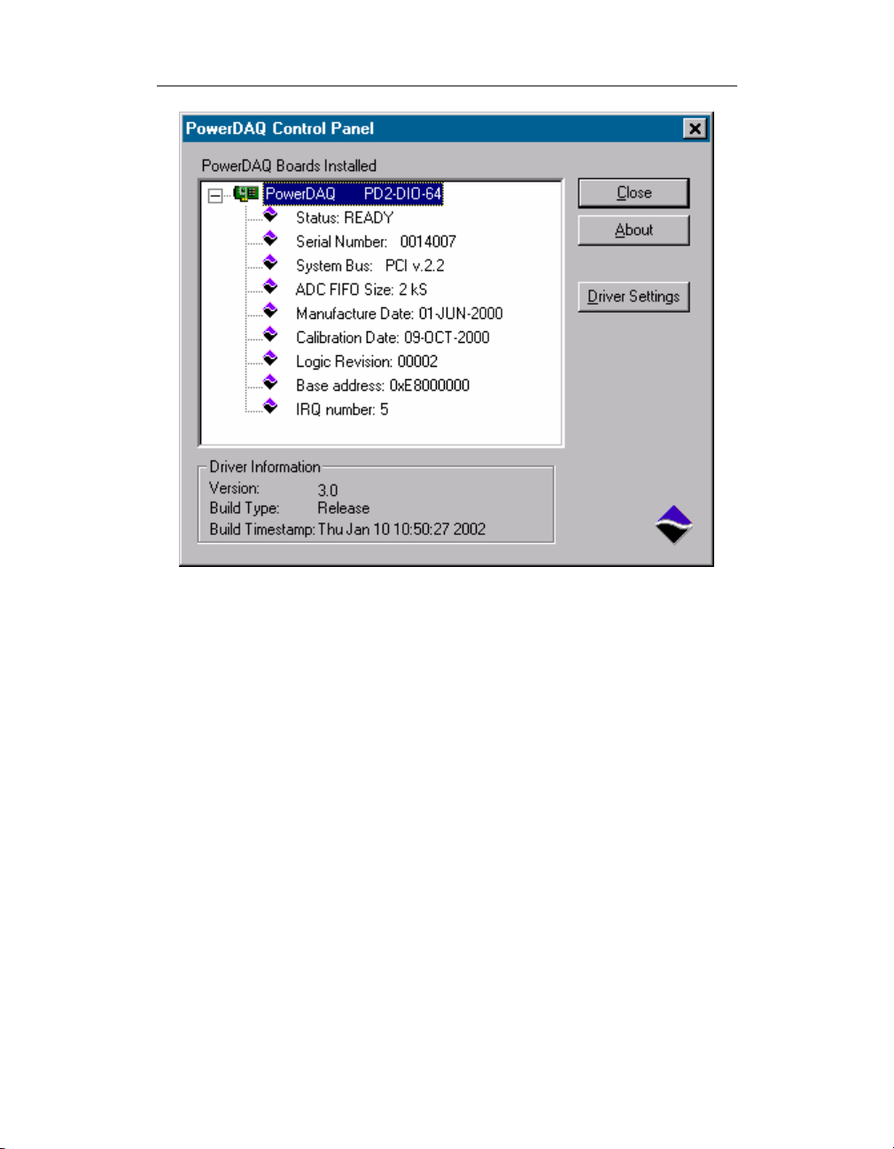
Control panel applet provides generic board information and does not
perform diagnostic of operation of on-board subsystems. The only
things you can verify with Control Panel is that the board is installed,
recognized by Windows and which resources are allocated by the
board. Also, you can see board model, serial number and
manufacturing/calibration dates.
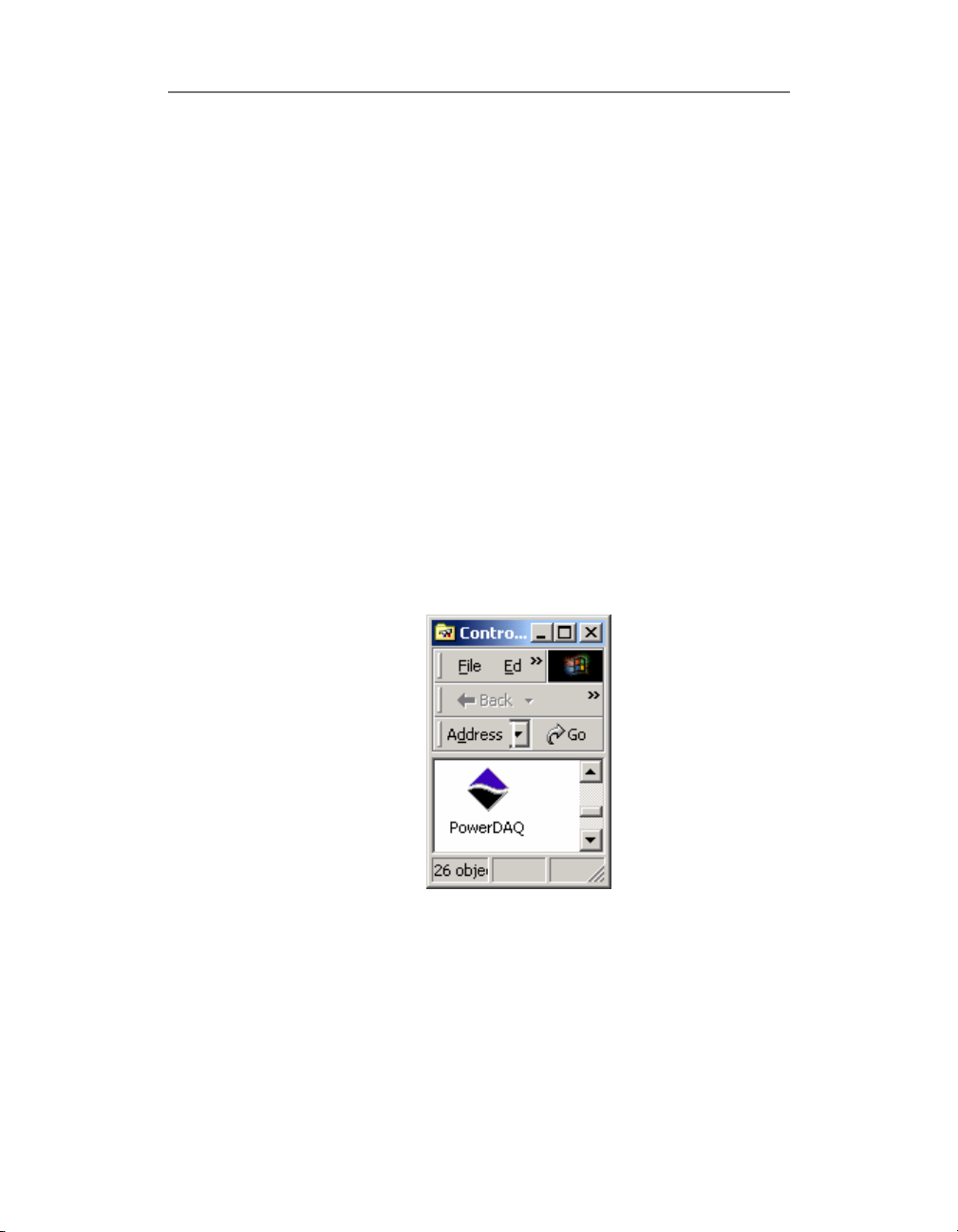
To access the PowerDAQ control panel, select START > Settings >
Control Panel and the PowerDAQ icon will be displayed.
14
Figure 1: Use the PowerDAQ ICON for quick diagnostics
Page 23
Chapter 2: Installation and Configuration
Figure 2: PowerDAQ control panel application showing PD2-DIO-
64 board installed
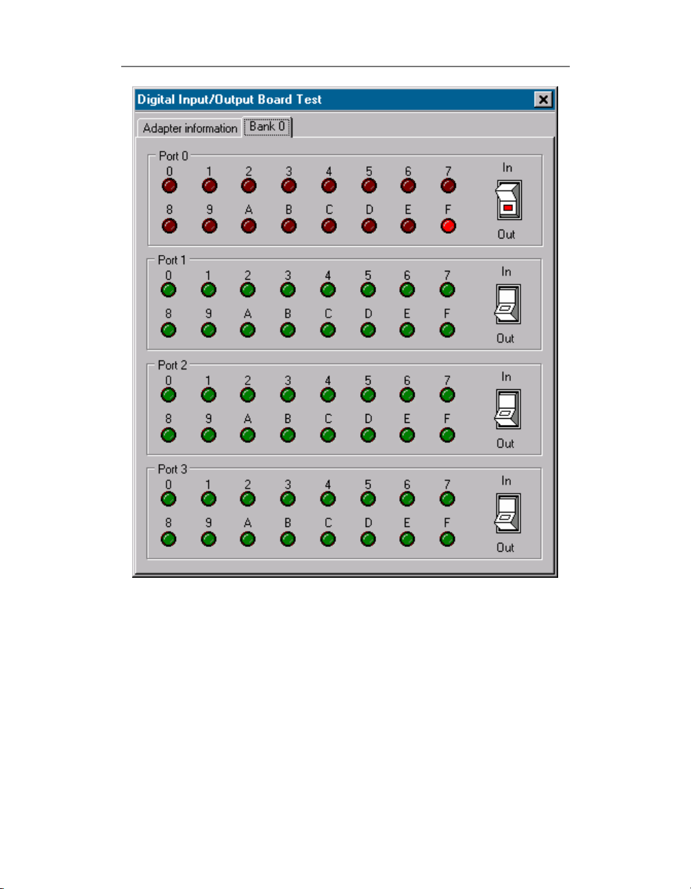
There is a diagnostic program supplied with PowerDAQ SDK called DIO
Test Application (DIOTest.exe). This program is located in PowerDAQ
program folder in Windows Start/Programs menu. You can run this
program and actually verify the functionality of the DIO. The program
performs “running light” test for every I/O, by default I/Os are
configured as an inputs, but if you will wire up the Port0 (DIO0..15) to
Port1(DIO16..31) and Port2(DIO32..47) to Port3(DIO48..63) using the
100 Ohm-1K resistors (PDL-DIO-STP provide jumpers to make the
connections above, but be careful and do not enable both ports,
connected together as an outputs because there are no current limiting
resistors on the PDL-DIO-STP-64).
15
Page 24
Chapter 2: Installation and Configuration
16
Figure 3: Digital I/O Board Test Application
Page 25

Chapter 2: Installation and Configuration
Hardware diagnostic procedure
Connect PowerDAQ DIO board to the screw terminal using the proper
cable (PD-DIO-CBL-100 for the PD2-DIO boards and PD-DIO-CBL-96
for all other models).
First thing you can measure is a presence of 5V power on the screw
terminal, which has 200mA maximum load capability (up to 1A option
is available, please contact factory for the details).
Also, you can attach the scope or logic analyzer to the certain I/Os, run
DIOTest application and check the output. The output of every enabled
channel should be seen as a positive pulse.
Subsystem- and application- specific examples
There are a numerous examples supplied with PowerDAQ SDK that
support PowerDAQ DIO boards. Please refer to readme file of the
latest installation and comments at the beginning of the main file of
each example you had installed for the details. Also, there is a
PowerDAQ Programming Manual available. That manual provides a
lot of detailed information about low level (C/C++) programming of
the PowerDAQ DIO boards and a numerous topics with general
information about PowerDAQ boards programming under the different
operating systems.
All PowerDAQ manuals are supplied in electronic Adobe Acrobat PDF
format. If you require the PDF reader, this can be downloaded from
the Internet at no cost from www.adobe.com
Following C/C++ examples are supplied with revision 3.x of PowerDAQ
SDK:
pddio_in.c - digital I/O single read example
pddio_ou.c - digital I/O single write example
pddi_buf.c - digital input stream (-ST boards only)
pdssi_ib.c - ESSI0 RX0 input stream
pddo_buf.c - digital output stream (-ST boards only)
pdssi_ob.c - ESSI0 TX0 output stream
pdct_evt.c - counter/timer events
pdct_buf.c - counter/timer (TMR0/TMR2) input stream (-CT only)
17
Page 26
Chapter 2: Installation and Configuration
pddi_evt.c - digital input events
dsp_irqs.c - high-speed interrupts (IRQA / IRQB / IRQC / IRQD)
essi_io.c - ESSI0/ESSI1 simple I/O access
pdsp_uct.c - highlights basic timer programming
Note The examples are also available for Visual BASIC and
Delphi.
Third-party software support
PowerDAQ SDK supports virtually every third-party software package,
available on the market. All advanced features of the PowerDAQ DIO
boards (timers/high-speed interrupts/buffered modes) are guaranteed
to be supported by C/C++/VB and Delphi. We are continuously
extending our third-party example base, thus please refer to installation
readme file for the complete list of the examples supplied. Please
contact OMEGA ENGINEERING technical support if you have any
specific questions about third-party software support.
18
Page 27

Chapter 2: Installation and Configuration
Accessories
PowerDAQ DIO boards are supplied with a large range of accessories:
• Cables
• Screw terminal panels
• Complete kits
• Signal Conditioning
• OEM distribution panel
Cables
Note To insure minimum (DIO only) board functionality
the following cables must be used, (depending on
the board model): PD2-DIO-64x – PD-DIO-CBL-100,
PD2-DIO-128x – 2 x PD-DIO-CBL-100.
PD2-DIO Series
The J1/J2 connectors use a 100-way 1-meter high-density IDC cable (PN
PD2-DIO-CBL-100).
The J3 connector uses a 16-way 18” twisted pair cable to connect
IRQ/Counter lines to the screw terminal or user board (PN PD2-DIOCBL-16).
The J4 and J5 connectors use a 26-way 18” twisted pair cable to
connect ESSI lines to the screw terminal or user board (PN PD2-DIOCBL-26).
Custom cables are available. Please contact your distributor or the
factory.
PDL-DIO Series
The J1 connector uses a 96-way 1-meter round shielded high-density
cable (PN PD2-DIO-CBL-96CE).
The J3 and J4 connectors uses specially designed splitter cable that
brings signals from those two connectors to the 37-way bracket and,
through this bracket, back to 14 (J3) and 26 (J4) connectors on the
PDL-DIO-STP-64 (PN PDL-DIO-CBL-37).
19
Page 28

Chapter 2: Installation and Configuration
Also separate cables PDL-DIO-CBL-16 (J3) and PDL-DIO-CBL-26 (J4)
may be used for the cost and/or space sensitive applications. In this
case cables may be pulled through the hole in the PCI bracket. To do
so, please unscrew the bracket, put the cables through the rectangular
hole in it and screw the bracket back to the board.
PDXI-DIO Series
The J1 connector uses a 96-way 1-meter round shielded high-density
cable (PN PDXI-CBL-96).
The J3 and J4 connectors uses specially designed splitter cable that
brings signals from those two connectors through the hole in cPCI
bracket, back to 14 (J3) and 26 (J4) connectors on the PDXI-DIO-STP64 (PN PDXI-DIO-CBL-37)
20
Page 29
Chapter 2: Installation and Configuration
Screw Terminal Panels
PD2-DIO Series
The PD2-DIO-STP-64 is a 64-channel screw terminal panel, which also
includes connections for the counter timers, high speed IRQ and ESSI
ports.
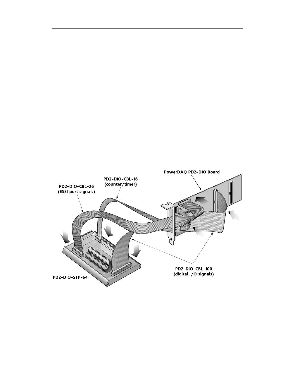
Figure 3 shows the typical connections between the PD2-DIO and PD2DIO-STP-64 terminal panel. Note that for 128-lines board one extra
PD2-DIO-STP-64 and PD-DIO-CBL-100 is required. Connections made
via PD2-DIO-CBL-16 are optional and this cable must be used only if
counter/timers or high-speed IRQs intended to be used. PD2-DIO-CBL26 is also optional and must be used only if ESSI subsystem operation is
considered by customer application.
Custom terminal panels are available. Please contact your distributor or
the factory.
Figure 4: PD2-DIO-STP-64 Wiring Diagram
21
Page 30

Chapter 2: Installation and Configuration
PDL-DIO and PDXI-DIO Series
The PDL-DIO-STP-64 is a 64-channel screw terminal panel, which also
includes connections for the counter timers, high speed IRQ and ESSI
ports. This STP panel utilizes 96-way Fujitsu connector for the
connectivity with PDL/PDXI DIO board DIO lines.
Figure 5: PDL-DIO-STP-64 Wiring Diagram
Connections on the Figure 5 applied to the PDL-DIO/PDXI-DIO series.
Connections made via PD2-DIO-CBL-16 are optional and this cable must
be used only if counter/timers or high-speed IRQs intended to be used.
PD2-DIO-CBL-26 is also optional and must be used only if ESSI
subsystem operation is considered by customer application.
Also, there is a combo solution available for the PDL-DIO board, when
two cables, PD2-DIO-CBL-26 and PD2-DIO-CBL-16 are replaced by one
cable/bracket solution: PDL-DIO-CBL-37.
22
Page 31

Chapter 2: Installation and Configuration
Complete kits
We have included the PD2-DIO-CBL-100 and the PD2-DIO-STP-64 into
a complete kit. The product is available by ordering PN PD2-DIO-STP64-KIT. This kit may be used with PD2-DIO boards only.
Connectors
J5 Connector J4 Connector
J3 Con nector
DSP
PowerDAQ
PCI Bus
PD2-DIO board
J1 Connector
J2 Connector
Figure 6: PowerDAQ PD2-DIO Connectors
J1/J2 Connector (PD2-DIO)
If you wish to develop you own custom cable, you can purchase the
connector and metal high-density IDC header from your distributor or
the factory. The part number is PD-ADM.
The manufacturer is Adam Technologies, Inc.
Telephone: 908-688-5000
Fax: 908-688-5001.
The manufacturers’ part number for the connector is HBHR-A-100-VSG
and the high-density IDC header HFCS-100-SG.
23
Page 32

Chapter 2: Installation and Configuration
J1 Connector (PD2-DIO)
24
Figure 7: Connector pin assignment for the J1 (PD2-DIO)
Page 33

Chapter 2: Installation and Configuration
J2 Connector (PD2-DIO-128 only)
Figure 8: Connector pin assignment for the J2 (PD2-DIO-
128)
25
Page 34

Chapter 2: Installation and Configuration
J4/J5 ESSI Connector (PD2-DIO)
Figure 9: Connector Pin Assignments for J4/5 (PD2-DIO)
Note J4/J5 Connector was designed to use either 26-way
IDC header for both ports or one 12-way IDC header
for the single port operations. For the combined
J4/J5 port the pin numbering is follows – 1..12 –
ESSI0 (J4), 13..14 – N/C, 15..26 – ESSI1(J5).
J3 Counter/Timers/IRQx Connector (PD2DIO)
26
Figure 10: Connector Pin Assignment for the J3 (PD2-DIO)
Page 35

Chapter 2: Installation and Configuration
1
J1 Connector
PDL-DIO board
PCI Bus
J3 Connector
DSP
PowerDAQ
Figure 11: PowerDAQ PDL-DIO Connectors
Low Noise DC-DC
J3 Connector
J4 Conne ctor
DSP
J4 Connector
PXI
J1 Connector
PowerDAQ
PDXI-DIO board
CompactPCI Bus
Figure 12: PowerDAQ PDXI-DIO Connectors
27
Page 36

Chapter 2: Installation and Configuration
J1 Connector (PDL/PDXI-DIO)
If you wish to develop you own custom cable, you can purchase the
connector and metal cover from your distributor or the factory. The
part number is PD-CONN.
The manufacturer is:
Fujitsu Takamisawa America, Inc.
Telephone: 408-745-4990 Fax: 408-745-4995
The manufacturers’ part number for the connector is FCN-230C096C/E and the metal cover FCN-247J096-G/E.
Custom terminal panels are available. Please contact your distributor or
the factory.
J3 Counter/interrupt Connector (PDL/PDXIDIO)
PowerDAQ board has a dedicated connector for the DSP counters and
interrupts, which is a 14-pin non-boxed 0.1” header on PD2-DIO boards
and 16-pin boxed 0.1” header on all other models.
In all cases mated IDC cable part number will be FCS-16-SG
The manufacturer is Adam Technologies, Inc.
Telephone: 908-688-5000
Fax: 908-688-5001.
J4 ESSI Connector (PDL/PDXI-DIO)
PowerDAQ board has a dedicated connector for the DSP ESSI ports,
which is a 2x12-pin non-boxed 0.1” header on PD2-DIO boards and 26pin boxed 0.1” header on all other models.
In all cases mated IDC cable part number will be FCS-26-SG
The manufacturer is Adam Technologies, Inc.
Telephone: 908-688-5000
Fax: 908-688-5001.
28
Page 37

Chapter 2: Installation and Configuration
J1 Connector (PDL/PDXI-DIO)
Figure 13: Connector pin assignment for the J1 (PDL/PDXI-DIO)
29
Page 38

Chapter 2: Installation and Configuration
J3 Counter/Timers/IRQx Connector
(PDL/PDXI-DIO)
Figure 14: Connector Pin Assignment for the J3 (PDL/PDXI-DIO)
J4 ESSI Connector (PDL/PDXI-DIO)
Figure 15: Connector Pin Assignments for J4 (PDL/PDXI-
DIO)
OEM Header Distribution Connector
The PD2-DIO-CONN64-4 distributes the 64 I/O’s lines into the
four sets 16 I/O lines via a 50-pin industry standard IDC connector.
These connectors may be attached directly into the standard relay
boards.
For 128 lines, you can connect two PD2-DIO-STP-64 or PD2DIO-CONN64-4 devices. Each connects to 64 lines via the high-density
100-pin ribbon cable (PD2-DIO-CBL-100).
30
Page 39

Chapter 2: Installation and Configuration
Figure 16: PD2-DIO-CONN wiring diagram
The PDL-DIO-CONN64-4 should be used instead of PD2-DIO-CONN644, when distribution of 64 lines to four sets of 16 lines via 50-way IDC
cable is required for the PDL-DIO or PDXI-DIO boards.
Custom terminal panels are available. Please contact your distributor or
the factory.
31
Page 40

Chapter 2: Installation and Configuration
32
Page 41

3
Architecture
Page 42

Chapter 3: Architecture
Architecture
This chapter describes the functional operation of the PowerDAQ DIO
boards.
Figures 17, 18 and 19 represent the block diagrams of PD2-DIO, PDLDIO and PDXI-DIO boards, respectively. Timed input/output streamed
access to the DIO subsystem is available on the –ST models only.
Counter/timer event streaming is implemented on the –CT models
only.
34
Figure 17: Block Diagram of the PowerDAQ PD2-DIO boards
Page 43

Chapter 3: Architecture
Figure 18: Block Diagram of the PowerDAQ PDL-DIO boards
Figure 19: Block Diagram of the PowerDAQ PDXI-DIO boards
35
Page 44

Chapter 3: Architecture
Functional Overview
All PowerDAQ DIO boards are based on the Motorola 56301 DSP with
full 32-bit 33MHz PCI support. All subsystems, except DIO are resides
on the DSP itself and accessible via PowerDAQ SDK functions. The DIO
subsystem is implemented as a set of 16-bit bi-directional registers with
overvoltage and ESD protection circuitry and pull-up resistors (PDL-DIO
and PDXI-DIO series only). Those registers are controlled by dedicated
logic that manages read/write access and provide direction control. DSP
is capable of monitoring all available input ports and interrupt host PC
on state change on any selected line with edge detection. Initial state
and direction of the DIO ports is programmed via software
(StartUpState program is supplied with PowerDAQ SDK) and stored in
the on-board EEPROM. It takes less, than 10mS after the system reset
to restore those values.
Following user subsystems are present on the DIO board:
• Digital Input
• Digital Output
• Counter-Timers
• Serial ESSI ports
• High-Speed Digital Interrupts
• Calibration/Startup configuration (EEPROM-based)
Difference between PD2-DIO and PDL-DIO boards is a board formfactor (PDL-DIO is a half-size of PD2-DIO) and a connector used.
PDXI-DIO moved form-factor into the CompactPCI standard and adds a
PXI compatibility.
DSP Processor
All PowerDAQ PD2-DIO boards are based on the Motorola 56301 DSP.
This is a 24-bit 66 MHz processor with an integrated PCI interface. The
PCI interface implements the PCI Local Bus Specifications so the board
is fully auto configured (base address, interrupt)
When the PowerDAQ DIO software is loaded, the PowerDAQ DIO
firmware is downloaded to the DSP via the PCI bus. This firmware
contains all the code necessary to communicate with the board
subsystems and the host PC driver.
36
Page 45

Chapter 3: Architecture
Note The drivers from the PowerDAQ web site always
contains the latest versions of the DSP firmware.
Please check www.Omega Engineeringdaq.com
the updates.
Note Custom programming of the DSP is not available
with the standard PowerDAQ DIO product. However,
should you require DSP processing, please consult
the factory.
for
PCI/PXI Bus Interface
The PowerDAQ DIO boards communicate via the PCI bus. The PCI bus
interface is embedded in the Motorola 56301 DSP. On power up, the
host PC automatically configures the boards’ base address and
interrupts resources.
PowerDAQ PDXI-DIO also incorporates support of PXI-TRIGx and
PXI_STAR lines according to PXI standard. Special software called PXI
Configurator supplied with PowerDAQ PDXI-DIO boards helps to
configure PXI bus. Also, all PXI configuration features are available via
the SDK function calls. Please note, that PXI configuration data is
stored into on-board EEPROM.
Digital Input and Output Subsystem (DIO)
The PowerDAQ digital input/output boards are configured as 64 or 128
(PD2-DIO only) lines. All boards use 16-bit line drivers, (not 8255
devices) which allow you to configure the start-up states in groups of
16-bit ports. Every port may be declared as input or output at start-up
and with user-defined default output value.
The DIO subsystem has different input modes, channel list options,
start and stop triggering and clocking control.
Also, every digital input may be configured to generate an interrupt on
any change of state on any line with edge detection. This is software
configurable.
37
Page 46

Chapter 3: Architecture
The digital I/O lines are capable of sinking up to 32mA at logic 1 and
64mA at logic 0 (guaranteed TTL levels). See datasheet at the end of
the manual for the details. This will support standard SSR and other
devices. Also, there is an option available for the +/-24mA registers
with guaranteed 4.2V output at 24mA, contact factory for the details.
ESSI
The Motorola 56301 DSP contains two High-Speed Enhanced serial
interfaces called ESSI. The PowerDAQ DIO board allows limited
buffered and unlimited register-based access depending upon the
board's operational mode. Each ESSI port contains three transmitters
and one receiver and has a maximum operational speed of 16.5 Mbit/s.
The slowest output bit rate based on DSP’s 66MHz clock is 16113bit/s.
In the combination with the PowerDAQ DIO software, the ESSI
subsystem can be used for High-Speed communication tasks. ESSI port
itself is an extremely flexible and may be adapted to the most of the
high-speed serial synchronous protocols available.
DSP Interrupt lines
Motorola DSP56301 is a powerful processor utilizing advanced Harvard
architecture. One of the features included on this processor is four
high-speed external interrupt lines. OMEGA ENGINEERING is pleased to
pass this feature along with the others to our customers.
38
Interrupt lines called IRQA/IRQB/IRQC/IRQD acts as
TIP
a part of initial system boot process. Those lines
must be properly pulled up or down (or left
unconnected/tri-stated) during the system boot-up
sequence. Following recommendations must be met
to allow you PC to boot properly. When IRQx lines
are used on the PowerDAQ: PD2-DIO revision I and
II : IRQA=1, IRQB / IRQC / IRQD = 0. All other
PowerDAQ DIO boards require IRQA=1, IRQB=0,
IRQC=0, IRQD = 1.
Page 47

Chapter 3: Architecture
Counter-timers
Depending on your PowerDAQ DIO board operation mode, the board
can support up to the three DSP based 24-bit counter/timers with
maximum count rate up to the 33 MHz for internal base clock and 16.5
MHz for the external clock. The minimum count rate is 0.00002 Hz for
the internal clock and has no bottom limit (but still require relatively
sharp, no longer than 1 ms, falling edge) for the external clock.
TIP
The software does not inform you directly which
counter/timers are available. To check the current
status of the timer you may check M_TE bit in the
timer status register using the _PdDSPRegRead
function.
Calibration and startup configuration
There is a critical requirement for the digital I/O board to have a
predictable output state during the start-up process. PowerDAQ DIO
boards provide an even more flexible way to define a start-up state of
every DIO channel on the board. To do so, start-up values along with
some other critical data are stored into on-board EEPROM. Those values
are loaded approximately 10mS after the rising edge of the system
reset signal. Also, for the PXI board, configuration of the PXI lines is
also stored into EEPROM. EEPROM has user accessible values and user
may potentially store some non-volatile data using applications. Because
EEPROM is a life-critical subsystem there are no examples provided for
such an access. Please consult factory if you consider EEPROM usage in
your applications.
39
Page 48

Chapter 3: Architecture
40
Page 49

4
PowerDAQ Software
Page 50

Chapter 4: PowerDAQ Software
PowerDAQ Software
PowerDAQ DIO board terminology
All DIO boards are visible to the external world as a set of 16-bit bidirectional registers called ports. Valid port numbers are 0 through 3
for the 64 channel boards (lines 0..15, 16..31, 32..47 and 48..63
respectively) and 0 through 7 for the 128 channel board (additional
four registers represents lines 64..79, 80..95, 96..111 and 112..127
respectively)
Clock relative to the DIO subsystem is either input clock for the input
timed operations or output clock for the output operations. Only one
port-register updated/read per one clock at the time. Clock may be
either external or internal for both input and output. External clock, if
used, must be connected via 100-200 Ohm resistors to the TMR1
terminal for the input operations and TMR2 terminal for the output
operations and expected to be a TTL pulses with minimum of 32nS of
duty cycle. When internal clock is used TMR1 and TMR2 is a
corresponding clock output and may be used for multiple board
synchronization purposes.
ESSI clock is a different type of clock, which represents the speed of
bit input/output stream operation and configured via ESSI registers.
ESSI clock is derived from the Motorola DSP based frequency, which is
a 66MHz and does not depend on TMR1/TMR2 programmed
frequency.
External latch is a dedicated input terminal, which may be used to
latch input data externally. It may be combined with external clock for
the effective operation. There is only one external latch terminal per
every 64-channles.
Propagate signal is a dedicated output which pulses every time when
selected ports are updated from the host (or DSP during the streaming
operation). It may be used for the handshaking purposes. This output is
a software-configurable. There is only one propagate terminal per every
64-channles, but it may be configured to show update of any
combination of the four available ports for every 64-channel connector.
42
Page 51

Chapter 4: PowerDAQ Software
Note Only –ST and –CT boards are suitable for the
streamed I/O operations with maximum clock
frequency up to 1600 KHz. Regular DIO boards
provide only static I/O that may be updated only
based on the PC clock. This will work only for the
update rates below 1000Hz under the Windows or
10000Hz under the Linux/QNX
43
Page 52

Chapter 4: PowerDAQ Software
Input/Output Mode
Single Update
The PowerDAQ DIO boards operate with either a single-update or
streaming input configuration. Single-update inputs/output mode
allows performing direct read/write access to any of the 16-bit ports of
the DIO board. Boards without –CT and –ST suffixes in the part
number will allow this mode only for the DIO and counter/timer
operations. The update frequency is limited by the PC and operating
system performance and generally in 1K-10K range (may be higher for
the real-time OS).
Note Single Update mode is easiest way for most of DIO
applications such as Relay Control or Sensor Read.
Also, Change of State Interrupt works perfectly fine
in combination with Single Update mode. S
Appendix D: Common Questions and Support.
The general sequence of the PowerDAQ SDK function calls for this
mode is:
ee
• Acquire all resources
• Open Driver
• Open Adapter
• Acquire Digital Input and/or Digital Output Subsystem
• Enable desired ports as an outputs
• Configure the events, if interrupts for the state change is used
• Read/Write the data from/to DIO ports
• Wait for the event to happens if interrupts are used
• Release all resources used
• Close subsystem
• Close Adapter
• Close driver
44
Page 53

Chapter 4: PowerDAQ Software
5
Steps 3-5 may be repeated indefinitely, steps 3 and 5 may be
unnecessary, depends on the specific application.
All the functions above may be easily combined to high-level versions.
C example for this mode is available and it is installed with PowerDAQ
SDK
pddio_in.c - digital I/O single read example
pddio_ou.c - digital I/O single write example
4
Page 54

Chapter 4: PowerDAQ Software
6
Event-based streamed I/O
Event-based streamed I/O mode allows continuous pattern generation
and is not limited by the amount of data. Every time the DSP based
FIFO is 1/2 full an interrupt is fired to request additional data be sent
to the board. The PowerDAQ advanced buffering mechanism hides
those interrupts from the user and allows you to work with big output
arrays logically divided by frames. The end of each frame can generate
an event, which will request more data from the application. Complete
information on the PowerDAQ advanced circular buffer (ACB) can be
found at www.Omega Engineeringdaq.com
Software Manual.
Note If the on-board FIFO is empty or the last value is
outputted, the output registers will continue to hold
the last value.
Input/Output buffer is organized as an array of 16-bit words or 32-bit
words (output), divided in certain number of logic blocks called
frames. Frames are divided into the scans. Scan is a set of samples –
one sample for every channel in the channel list. Number of frames
depends on the specific applications. Usually, four frames are a good
choice for most cases. A bigger number of smaller frames allows to
scan data more often but frame size should not be smaller, than 512
samples for the input and 1024 samples for the output. Also, there is
an option to read/write the whole buffer only once when driver will
stop acquisition automatically at the end of the buffer. Following
constants, combined together, are define the buffer behavior in
_PdAcquireBuffer API function:
and in the PowerDAQ SDK
AIB_DWORDVALUES – use 32-bit DWORD data where lower
16 bits represents the actual data and bits 16..18 represents the output
port number (0..7). Valid for output buffered mode only.
AIB_BUFFERWRAPPED – allow driver to use buffer more, than one
time. If this flag is not set the driver will stop acquisition at the end of
the buffer and will set the corresponding flags (
eStopped
AIB_BUFFERRECYCLED – overwrite the data in the buffer even if old
data has not been read/updated yet.
4
) in the application event.
eBufferDone
and
Page 55

Chapter 4: PowerDAQ Software
7
AIB_FIXEDDMA – use fixed channel list mode (1/2/4/8 channels
only), input mode, default.
AOB_DMAEN – use fixed channel list mode (1/2/4/8 channels only),
output mode, default, must be part of the configuration word for the
_PdDOAsyncInit call.
Following steps are required for the event-based mode:
• Acquire all resources
• Open Driver
• Open Adapter
• Acquire Digital Input and/or Digital Output Subsystem
• Acquire Buffer
• Enable desired ports as an outputs
• Configure the events (eFrameDone/eBufferDone and all error
events must be reported)
• For the output – fill the buffer with initial data
• Enable I/O
• Process the data in event-based loop
• Wait for the event to happens if interrupts are used
• Check the event and, if data is available (or more space in the
output buffer)
• Read/Write data to/from the buffer
• Re-enable events
• Release all resources used
• Release Buffer
• Close subsystem
• Close Adapter
• Close driver
Following examples are supplied with PowerDAQ SDK 3.x which
supports various input/output buffered modes :
pddi_buf.c - digital input stream (-ST boards only)
pddo_buf.c - digital output stream (-ST boards only)
4
Page 56

Chapter 4: PowerDAQ Software
Auto-regeneration output (pattern regeneration)
Some testing and control application require a continuous regeneration
of the same output pattern. For these purposes PowerDAQ DIO board
defines an especially dedicated mode, called auto-regeneration I/O.
Auto-regeneration mode can be used to create fixed length patterns
without any host intervention of user software after the subsystem has
initialized. An application writes data to the buffer of the PowerDAQ
driver board and each time the end of buffer is reached, it starts to resend the same buffer again. Note, that 2048 samples can fit into the
on-board DSP memory and auto regeneration of up to 2048 samples
will not require any intervention of the host PC.
Auto-regeneration is basically subset of a buffered output mode and
every buffered output example may be easily modified to the
regenerate mode.
Example, listed below may be easily modified to work in regenerate
mode, modification require only change of couple of defines and well
commented in the example source code:
pddo_buf.c - digital output stream (-ST boards only)
48
Page 57

Chapter 4: PowerDAQ Software
DIO Channel List
There are two channel list modes available on the PowerDAQ DIO
boards:
• continuous unlimited length channel list
• fixed length channel list
First option provides most flexible solution, available on the market, to
the customer. In this case, every output sample is accomplished by
read/write port number. The only trade-of is a performance limitation
(500KS/sec upstream / downstream maximum). This mode is turned
on by disabling AIB_FIXEDDMA flag in _PdAcquireBuffer function call.
Second option is available when higher input/output rates (up to
1600KS/sec) are required. In this case, only 1/2/4 or 8 sequential
channels in the channel list are available for the streamed I/O
operation. Acquisition may be started from any available on the DIO
board ports. Example: channels 3/4/5/6 are acquired in the co-called
DMA buffered mode on the PD2-DIO-64ST board. In this case channels
0,1,2,7 are still available for the non-buffered operation.
The Channel List is a powerful feature of the PD2/PDL/PDXI-DIO board
when properly used by user application.
Note Both channel list modes may be combined with any of
the buffered I/O modes available.
49
Page 58

Chapter 4: PowerDAQ Software
0
Digital Input Change-Of-State interrupts
One of the powerful features of the PowerDAQ DIO boards is an
ability to detect state change on any of the selected input line and
optionally interrupt the host PC when those conditions are detected.
The way this feature implemented guarantees minimum possible
response time for the digital input change – all unused time of the DSP
is dedicated to the state change detection process. Usually, the
minimum width of the detected signal is 1uS for all 128 lines and 0.2uS
for the 16 lines.
Change-of-state interrupt subsystem is represented to the used
software as a set of 16-bit arrays each of them has a eight entries
corresponding to the ports 0 through 7. Those arrays are Interrupt
Mask, Interrupt Data and Edge Data. Interrupt mask is only array
configured by the user. It should have one in every bit corresponding to
the input line, where user software is interested in getting interrupt
when this line changes its state. Interrupt Data array returns one for
every bit, which was not masked (0 in Interrupt Mask), and changes its
state since interrupts were enabled. Interrupt Edge array contains one
for the rising edge and zero for the falling edge, but only those bits
are valid that have a corresponding bit set to one in Interrupt Data
array.
Generally, interrupts are initialized in the following sequence
(driver/board initialization not included) :
• Define direction of the I/O ports
• Create Interrupt Mask array
• Enable Interrupts
• Wait for the interrupt
• Every time, when interrupt is happens, read Interrupt Data/
Interrupt Edge arrays and re-enable interrupt
• Stop this process, when required
pddi_evt.c example shows how to use this powerful feature.
5
Page 59

Chapter 4: PowerDAQ Software
Timing and Control
The PowerDAQ DIO clocking and triggering features are extensive and
can be configured in different ways.
Digital Input/Output Clocking
Clocking comprises of two input signals
1. Input clock – used to clock digital input channels in
channel list.
2. Output clock – used to clock digital output channels in
channel list.
You must load the channel list prior to starting the acquisition. Note,
that only –CT and –ST boards support the clocked I/O operations.
Clocking can be controlled by
• Internal Clock (DSP)
• External Clock
• Software clock (non-timed operation only)
External trigger
Digital input and output streamed operation along with ESSI and
counter stream may be triggered by the external event. This event must
be supplied by the customer hardware. IRQC terminal is used as trigger
input. Trigger signal must be a TTL-level signal. Negative, at least 20
nS long, pulse may be used to start and/or stop acquisition. Actual
trigger is detected on the negative (1-0) edge of the incoming trigger
signal. If both start and stop triggers are enabled first pulse will start
acquisition and following will stop it and so on.
Note Maximum trigger line frequency should not exceed
1 kHz to insure proper operation of the DIO board,
but minimum space between two given triggers may
be as short as 1 µS.
51
Page 60

Chapter 4: PowerDAQ Software
2
PD-DIO-CBL-16 or equivalent must be used to connect PDx-DIO board
J3 connector to the PDx-DIO-STP-64 when external trigger is used.
Trigger source must be connected to the IRQC terminal on the PDxDIO-STP-64 via 200-Ohm current-limiting resistor. See high-speed
interrupt section for more details about IRQ handling.
External trigger is set via software using the xx_STARTTRIGx and
xx_STOPTRIGx constants ORed together with other settings in the
/ _
configuration word for the PdDOAsyncInit
calls.
Every buffered example contains comments about how to use external
trigger.
PdDIAsynInit function
External clock
Digital input and output streamed operation may be programmed to be
clocked by an external clock source. This clock must be supplied by the
customer hardware. TMR1 terminal is used as clock input for the input
streamed operations and TMR2 terminal is used for the output
streamed operations. Clock signal must be a TTL-level signal. Negative,
at least 20 nS long
Note Maximum clock frequency should not exceed 500 kHz
in the unlimited channel list mode and 1600 kHz for
the fixed channel list mode. PD-DIO-CBL-16 or
equivalent must be used to connect PDx-DIO board
J3 connector to the PDx-DIO-STP-64 when external
clock is used.
External clock is set via software using the xx_CVSTARTx constants
ORed together with other settings in the configuration word for the
PdDOAsyncInit
and examples sources for the details.
Clock source must be connected to the TMR1/2 terminal on the PDxDIO-STP-64 via 200-Ohm current-limiting resistor.
5
/ _
PdDIAsynInit function calls. See programmer manual
Page 61

Chapter 4: PowerDAQ Software
Synchronizing two or more boards
Some applications require multiple board synchronization. PDXI-DIO
board has more options for the inter-board synchronization, which
includes PXI bus and external connections via the cables. All other
boards allow synchronization based only on external cabling
connections.
Note Using the PowerDAQ ™ control panel applet; please
ensure the software driver recognizes the two or
more PowerDAQ boards. Custom synchronization
connections are required.
Wiring requirements:
The PowerDAQ DIO J3 internal connector has a TMRx Clock Output pin.
When internal clock is set via the software TMR1 represents output
clock for the input streaming operations and TMR2 represents output
clock for the output streaming operations. You can connect
corresponding pin to the TMRx pin of the next board you wish to
synchronize acquisition. Also, you may synchronize PDx-DIO board with
any of the other available PowerDAQ boards including multifunction,
PDL-MF and analog output series.
When synchronization is required for the PDXI-DIO boards all
connections may be set via PXI bus using the PXI_TRIGx lines. Please
use PXI Configurator software to do this.
53
Page 62

Chapter 4: PowerDAQ Software
Enhanced Serial Interfaces (ESSI)
Basically ESSI port has input and output data lines, input and output
clock lines and input and output frame synchronization lines. Frame is 1
to 32 data words. Data word length is 8/12/16/24 and 32 bits. 32-bit
mode doesn’t use either most or least significant byte (MSB/LSB). Also
operational mode includes normal and network modes. Network mode
adds one extra bit clock after every frame for the synchronization. The
I/O and clock polarity is programmable via the software.
PowerDAQ SDK provides two access levels to the ESSI ports.
Easiest way is to program ESSI registers directly using the DSP access
functions:
set of necessary constants and complete example essi_
shows how to access ESSI port on this level. This mode does not
support interrupts – user application must pull readiness bits in the ESSI
registers to insure the data transfer integrity.
The second way is to use limited buffered ESSI0 support, which is
provided by the high-level PowerDAQ SDK functions. In this case
transfer speeds up to 1.05Mword/sec supported which leads to
16.5Mbit/s ESSI bit rate. In this mode TX0 output and RX0 inputs with
full clock and frame synchronization supported. TX and RX subsystems
are semi-independent and may be used simultaneously.
PdDSPRegRead and PdDSPRegWrite. PowerDAQ SDK provide
io.c which
Note TX subsystem in buffered mode shares some
resources with digital output in buffered mode and
they are mutually exclusive. The same is true for the
RX subsystem and digital input or counter-timer
event input modes. Thus, when you decide to use
ESSI subsystem on the –ST or –CT boards, please
make sure that you are not creating a conflict with
the existing software.
Note PD-DIO-CBL-26 or equivalent must be used to
connect PDx-DIO board J4 connector to the PDxDIO-STP-64, when ESSI features are used.
Following examples are supplied with PowerDAQ SDK 3.x which
supports ESSI input/output buffered modes:
54
Page 63

pdssi_ib.c - ESSI0 RX0 input stream
pdssi_ob.c - ESSI0 TX0 output stream
Please refer to the example sources and the
TIP
Motorola DSP56301 DSP user manual (Motorola PN
DSP565301UM) for the details about ESSI port
programming. Also, there are useful applications
notes (AN1764) available from the Motorola’s website www.mot.com
Chapter 4: PowerDAQ Software
55
Page 64

Chapter 4: PowerDAQ Software
Counter/Timer Subsystem
Counter/timer subsystem has three 24-bit counters, and common 20bit optionally used divider called pre-scaler. Each counter has a set of
it’s own load/count/status and compare registers. Please refer to the
example sources and Motorola DSP56301 DSP user manual (Motorola
PN DSP565301UM) for the details about DSP counter/timer
programming.
Counters named TMR0, TMR1 and TMR2. Each timer can use internal
or external clocking and can interrupt the DSP56301 after a specified
number of events (clocks) or can signal an external device after
counting internal events. Each timer connects to the external world
through a single bi-directional pin TIOx that is 7kV ESD and +/-30V
overvoltage protected. When TIOx is configured as input the timer
functions as an external event counter or can measure external pulse
width/signal period. When TIO is used as output the timer is
functioning as either a timer, a watchdog or a Pulse Width Modulator.
Some common timer/counter/output functions which microprocessors
require are:
• Real time clock,
• Event counter
• Digital one-shot
• Programmable rate generator
• Square wave generator
• Binary rate multiplier
• Complex digital wave form generator
• Complex motor control
DSP Counter/timers are used by –ST and –CT boards to define a timebase for input and output streamed operations. TMR1 counter is used
for the buffered input modes such as buffered digital input and
buffered counter-timer external event streaming. TMR2 is a time-base
for the digital output buffered mode. TMR0 and/or TMR1 may be also
a source (counters, counting events) for the counter stream operation
on the –CT board.
56
Page 65

Chapter 4: PowerDAQ Software
Each counter is a 24-bit count-up counter, after power-up, the count
value and output of all counters is set to zero. Each counter must be
programmed before it can be used; unused counters need not be
programmed. Counters are programmed by using the PowerDAQ SDK.
Each counter is fully independent of the others except all counters
share the same pre-scaler. Each counter may operate in a different
mode.
PowerDAQ SDK provides a set of examples for the DSP counter/timers.
pdct_evt.c example highlights use of interrupts for the external event
counting. pdct_buf.c example shows, how to use counter/timer stream
mode on the –CT boards. pdsp_uct.c example highlights just a basic
timer programming.
57
Page 66

Chapter 4: PowerDAQ Software
High-Speed interrupts
A high-Speed interrupt line is powerful feature of the PowerDAQ DIO
boards.
IRQ lines act as a part of the Digital input subsystem and use the same
mechanism as digital input change-of-state interrupts uses. IRQ reacts
to the external event in 100nS and interrupt the host PC in less, than
1uS but host PC reaction depends on the current system load and
operational system used.
IRQx terminal detects only negative edge of the incoming signal. The
minimum length of the negative pulse must be at least 20nS to be
properly detected by the board.
Please note, that IRQC terminal is used also as an external trigger input
and IRQD terminal used as a service input (connected to TMR1 output),
when events from the TMR2 counter streamed on the-CT board.
PD-DIO-CBL-16 or equivalent cable must be used to connect PDx-DIO
J3 connector to the PDx-DIO-STP-64 when high-speed IRQs are used.
See dsp_irqs.c example for the details.
58
Page 67

5
Appendixes
Page 68

Appendixes
0
Appendix A: Specifications
PowerDAQ DIO specifications:
All external I/O on the PowerDAQ DIO boards are 7 kV ESD protected
and +35/-5v Overshoot/Undershoot protected. PDL-DIO and PDXI-DIO
models provide 10Kohm pull-ups on all I/O lines. They may be
optionally left unpopulated based on customer request.
IO subsystem
64 lines of digital I/O in four 16-bit ports or 128 lines of digital I/O in
eight 16-bit ports
DC Electrical Characteristics over Operating Range
The Following Conditions Apply:
T
A
= –40°C to +85°C
Parameter Test conditions Result
Input High Level Guaranteed logic 2.0V min
High level
Input Low Level Guaranteed logic 0.8V max
Low level
Input High Current VI = 5V ±1 µA max
Input Low Current VI = Gnd ±1 µA max
3-State Output Current VO = 2.7V ±1 µA max
3-State Output Current VO = 0.5V ±1 µA max
Short-Circuit Current VO = Gnd -80 mA min
-140 mA typ
-250 mA max
Input Hysteresis 100 mV typ
Note The maximum I/O rate for –CT boards are
1600 kS/s for fixed CL-mode and 500 kS/s for
unlimited CL-mode. PC-timed update: 1000 Hz – 10
kHz.
6
Page 69

Appendixes
Output Drive Characteristics:
Parameter Test conditions Result
Output Drive Current VO = 2.5V -32 mA per pin
-180 mA per port
Output High Voltage IOH = -3 mA 3.5V typ, 4.8V max
Output High Voltage IOH = -15 mA 3.5V typ, 4.7V max
Output High Voltage IOH = -32 mA 2.4V min, 3.0V typ
Output Low Voltage IOL = 64 mA 0.2V typ, 0.55V max
I/O Power Off Leakage V I/O @ 4.5V ±1 µA max
Counter/Timer Specifications:
The following conditions apply:
A
= –40°C to +100°C; C load = 50pF + 2 TTL loads
T
Parameter Value
Number of Channels 3
Resolution 24 bits
Maximum Frequency 16.5 MS/s for external clock and
33 MS/s for internal DSP clock
Minimum Frequency
Minimum Pulse Width 20 ns
Output High Level 2.0V min @ -4 mA
Output Low Level 0.5V max @ 4 mA
Protection
Input Low Voltage 0.0–0.8V
Input High Voltage 2.0–5.0V
0.00002 S/s for internal clock, no
low limit for external clock
7 kV ESD,
±30V overshoot/undershoot
Note The maximum event stream rate for –CT boards are
1.2 MS/s.
61
Page 70

2
ESSI Specifications:
Parameter Value
Number of Channels 2
Resolution 8/12/16/24
Maximum Rate 16.5 Mb/s
Minimum Rate 16.113 b/s
low limit for external clock
Minimum Pulse Width 20 ns
Output High Level 2.0V min @ -4 mA
Output Low Level 0.5V max @ 4 mA
Protection 7 kV ESD,
±30V overshoot/undershoot
Input Low Voltage 0.0–0.8V
Input High Voltage 2.0–5.0V
Appendixes
6
Page 71

Appendixes
Appendix B: Digital Signal
Conditioning
General Description
All PowerDAQ boards can control solid-state relays when
combined with PD-SSR series modules, which are available as
inputs for sensing changes or as outputs to send TTL signals
for control purposes.
The PD-SSR senses logic levels and sends results to the
PowerDAQ DIO subsystem. It also detects and reports opens
and shorts. PD-SSR modules plug into a 16-channel
backplane (PD2-DIO-BPLANE-16).
Up to four backplanes can connect to the PowerDAQ digital
distribution panel (PD2-DIO-CONN64-4 or PDL-DIOCONN64-4), which distributes 64 lines into four groups of
16. For the PD2-DIO-128 you can use up to two PD2-DIOCONN-64-4 panels.
The PD2-DIO-CONN64-4 and PDL-DIO-CONN64-4 are DIN
mountable and also has 5V, digital ground, latch and update
signals.
The PowerDAQ Software Suite includes extensive software
support for controlling and reading the digital signalconditioning products. Support is included for Visual C++,
Delphi, Visual Basic, Borland C++, LabVIEW, TestPoint,
DASYLab, Agilent VEE and DIAdem software.
63
Page 72

Technical Specifications
Digital Input Modules
Appendixes
Ordering Nominal Input Max
Information Input Voltage Current Current Time Time
PD-SSR-IAC-5 120V AC 90–140V 10 mA 16 mA 20 ms 30 ms
PD-SSR-IAC5A
PD-SSR-IDC-5 3.3–32V
240V AC 120–280V 10 mA 16 mA 20 ms 30 ms
DC
3.3–32V
DC
Input
32 mA 16 mA 1 ms 1 ms
Max
5V DC
Max
TurnOn
Max
TurnOff
Digital Output Modules
Ordering Nominal Output Maximum Max
Information Output Voltage Output Current Time
Voltage Range Current
PD-SSR-OAC-5 120V AC 24–140V
PD-SSR-OAC5A
PD-SSR-ODC-5 3–60V DC 3–60V DC 3.0A 16 mA 25 µs (on)
50 µs (off)
240V AC 120–280V 3.5A 19 mA 0.5 cycles
AC
3.5A 18 mA 0.5 cycles
5V DC
Response
64
Figure 20: PD2-DIO-CONN wiring diagram
Page 73

Appendixes
5
Appendix C: Dimensions
Dimensions:
The following table contains the dimensions of the PowerDAQ DIO
boards and accessory products.
Product Dimensions (W x L x H)
PD2-DIO-xx 4.2” x 8.6” x 0.5”
PDL-DIO-xx 4” x 5” x 0.5”
PDXI-DIO-xx 4” x 7” x 0.5”
PD2-DIO-STP-64 4.4” x 7.1” x 2.1”
PD2-DIO-CONN64-4 4.4” x 7.1” x 2.1”
PDL-DIO-STP-64 4.4” x 7.1” x 2.1”
PDL-DIO-CONN64-4 4.4” x 7.1” x 2.1”
PDXI-DIO-STP-64 4.4” x 7.1” x 2.1”
PDXI-DIO-CONN64-4 4.4” x 7.1” x 2.1”
6
Page 74

Appendixes
6
Appendix D: Common
Questions and Support
What is PCI Specification 2.1?
Q
A
The PCI LocalBus is a high-performance bus that provides a
processor-independent data path between the CPU and highspeed peripherals. PCI is a robust interconnect mechanism
designed specifically to accommodate multiple high performance
peripherals for graphics, full motion video, SCSI, LAN, etc.
The PCI Local Bus Specifications, Rev 2.1 includes the protocol,
electrical, mechanical and configuration specification for the PCI
Local Bus components and expansion boards.
The Rev 2.1 was published June 1, 1995 by the PCI Special Interest
Group.PO Box 14070,Portland,OR 97214. Web site:
www.pcisig.com
Q
How often should I calibrate my board?
A
The PD2-DIO series board does not required any calibration
procedure`.
6
Page 75

Appendixes
Service and Support
If you have technical problems using PowerDAQ PD2-DIO, our Technical
Support department can be reached by:
Telephone: (781) 821 2890
Fax: (781) 821 2891
Email: support@powerdaq.com
Web Site: www.powerdaq.com
For the most efficient service, please be available at your computer and
be prepared to answer several questions listed on the following page
when you call for technical support. This information helps us identify
specific system and configuration-related problems.
67
Page 76

Appendixes
Technical Support Form
Photocopy this form and update it each time you make changes to
your software or hardware. Completing this form accurately before
contacting us for technical support helps our application engineers
answer your questions more efficiently.
What is the name and version number of the product?
____________________________________________
What version of Windows are you using?
____________________________________________
What programming language and version?
____________________________________________
Is the board set at factory configuration?
____________________________________________
Have you run the board diagnostics? What were the results?
____________________________________________
Did the system ever work ? If so, what changed (moved location,
installed other boards, software etc..)
____________________________________________
Have you run the sample programs? What were the results?
____________________________________________
Have you verified that all your connections are made properly and
are secure?
____________________________________________
Have you been able to isolate the source of your problem: input or
output device, board, software?
____________________________________________
What other boards or applications are installed in your system?
____________________________________________
How much RAM do you have?
____________________________________________
What size hard disk are you using?
____________________________________________
How fast is your CPU?
____________________________________________
How fast is your host data bus?
____________________________________________
If you are on a network, what type of network are you using and
approximately how many users are on the network?
____________________________________________
Please specify whether or not the problem occurred more than once
____________________________________________
68
Page 77

Appendixes
Appendix E: Warranty
Overview
IBM, IBM PC/XT/AT and IBM PS/2 are trademarks of International
Business Machine Corporation.
BASIC is a trademark of Dartmouth College.
Microsoft is a trademark of Microsoft Corporation.
LabVIEW, LabWindows/CVI is a trademark of National Instruments
Corporation
All PowerDAQ PD2-DIO boards have received CE Mark certification
according to the following:
• EN55011
• EN50082-1
Life Support Policy
OMEGA ENGINEERING' PRODUCTS ARE NOT AUTHORIZED FOR USE AS
CRITICAL COMPONENTS IN LIFE SUPPORT DEVICES OR SYSTEMS
WITHOUT THE EXPRESS WRITTEN APPROVAL OF THE LEGAL AFFAIRS
DEPARTMENT OF OMEGA ENGINEERING CORPORATION. As used
herein:
1. Life support devices or systems are devices or systems which, (a) are
intended for surgical implant into the body, or (b) support or sustain
life, and whose failure to perform, when properly used in accordance
with instructions for use provided in the labeling, can reasonably be
expected to result in a significant injury to the user or (c) should the
device or system fail to perform, may reasonably be expected to result
in a significant hazard to human life, or a significant potential for
injury to the user.
2. A critical component is any component of a life support device or
system whose failure to perform can be reasonably expected to cause
the failure of the life support device or system, or to effect its safety
or effectiveness.
69
Page 78

Appendixes
Omega Engineering, inc. warrants that the products furnished under
this agreement will be free from material defects for a period of one
year from the date of shipment. The customer shall provide notice to
Omega Engineering of such defect within one week after the
Customer’s discovery of such defect. The sole obligation and liability of
Untied Electronic Industries under this warranty shall be to repair or
replace, at its option, without cost to the Customer, the product or part
which is so defective and as to which such notice is given.
Upon request by Omega Engineering, the product or part claimed to be
defective shall immediately be returned at the customer’s expense to
Omega Engineering.
There shall be no warranty or liability for any products or parts which
have been subject to misuses, accident, negligence, failure or electrical
power or modification by the Customer without Omega Engineering’
approval. Final determination of warranty eligibility shall be made by
Omega Engineering. If a warranty claim is considered invalid for any
reason, the Customer will be charged for services performed and
expenses incurred by Omega Engineering in handling and shipping the
return item.
As to replacement parts supplied or repairs made during the original
warranty period, the warranty period of the replacement or repaired
part shall terminate with the termination of the warranty period with
respect to the original product or part.
THE FOREGOING WARRANTY CONSTITUTES UNTIED ELECTRONICS
INDUSTRIES SOLE LIABILITY AND THE CUSTOMER’S SOLE REMEDT
WITH RESPECT TO THE PRODUCTS AND IS IN LIEU OF ALL OTHER
WARRANTIES. LIABILITIES AND REMEDIES, EXCEPT AS THUS
PROVIDED, OMEGA ENGINEERING DISCLAIMS ALL WARRANTIES,
EXPRESSED OR IMPLIED, INCLUDING ANY WARRANTY OF
MERCHANTABILITY OR FITNESS FOR A PARTICULAR PURPOSE.
70
Page 79

Glossary
Glossary
A
Asynchronous (1) Hardware - A property of an event
that occurs at an arbitrary time,
without synchronization to a reference
clock.
(2) Software - A property of a function
that begins an operation and returns
prior to the completion or termination
of the operation.
B
Background Acquisition Data is acquired by a DAQ system
while another program or processing
routine is running without apparent
interruption.
Base Address A memory address that serves as the
starting address for programmable
registers. All other addresses are
located by adding to the base address.
Bit One binary digit, either 0 or 1.
Block-Mode A high-speed data transfer in which
the address of the data is sent
followed by a specified number of
back-to-back data words.
Burst-Mode A high-speed data transfer in which
the address of the data is sent
followed by back-to-back data words
while a physical signal is asserted.
Bus The group of conductors that
interconnect individual circuitry in a
computer. Typically, a bus is the
expansion vehicle to which I/O or other
devices are connected. Examples of PC
buses are the ATPCI Bus.
71
Page 80

Glossary
Bus Master A type of a plug-in board or controller
with the ability to read and write
devices on the computer bus.
Byte Eight related bits of data, an eight-bit
binary number. Also used to denote the
amount of memory required to store
one byte of data.
C
Cache High-speed processor memory that
buffers commonly used instructions or
data to increase processing throughput.
Channel List A variable length list of 1 to 8
channels/ports
Control Register(s) Registers containing control bits to
initiate control signals to various
onboard subsystems.
Code Generator A software program, controlled from
an intuitive user interface that creates
syntactically correct high-level source
code in languages such as C or Basic.
Component Software An application that contains one or
more component objects that can
freely interact with other component
software. Examples include OLEenabled applications such as Microsoft
Visual Basic and OLE Controls for
virtual instrumentation in Component
Works.
Counter/Timer A circuit that counts external pulses or
clock pulses (timing), such as the Intel
8254 device.
Coupling The manner in which a signal is
connected from one location to
another.
Crosstalk An unwanted signal on one channel
due to an input on a different channel.
72
Page 81

Glossary
Current Sinking The ability of a DAQ board to dissipate
current for analog or digital output
signals.
Current Sourcing The ability of a DAQ board to supply
current for analog or digital output
signals.
D
DAQ Data Acquisition
(1) Collecting and measuring electrical
signals from sensors, transducers, and
test probes or fixtures and inputting
them to a computer for processing;
(2) Collecting and measuring the same
kinds of electrical signals with A/D
and/or DIO boards plugged into a PC,
and possibly generating control signals
with D/A and/or DIO boards in the
same PC.
dB Decibel The unit for expressing a
logarithmic measure of the ratio of two
signal levels: dB=20log10 V1/V2, for
signals in volts.
DIO Digital input/output.
DLL Dynamic Link Library A software
module in Microsoft Windows
containing executable code and data
that can be called or used by Windows
applications or other DLLs. Functions
and data in a DLL are loaded and linked
at run time when they are referenced
by a Windows application or other
DLLs.
DMA Direct Memory Access: A method by
which data can be transferred to/from
computer memory from/to a device or
memory on the bus while the processor
does something else. DMA is the
73
Page 82

Glossary
fastest method of transferring data
to/from computer memory.
Drivers Software that controls a specific
hardware device, such as DAQ boards.
DSP Digital signal processing.
Dual-Access Memory Memory that can be sequentially
accessed by more than one controller
or processor but not simultaneously
accessed. Also known as shared
memory.
Dual-Ported Memory Memory that can be simultaneously
accessed by more than one controller
or processor.
Dynamic Range The ratio of the largest signal level a
circuit can handle to the smallest signal
level it can handle (usually taken to be
the noise level), normally expressed
indB.
E
EEPROM Electrically Erasable Programmable
Read-Only Memory ROM that can be
erased with an electrical signal and
reprogrammed.
Encoder A device that converts linear or rotary
displacement into digital or pulse
signals. The most popular type of
encoder is the optical encoder, which
uses a rotating disk with alternating
opaque areas, a light source, and a
photo detector.
EPROM Erasable Programmable Read-Only
Memory: ROM that can be erased
(usually by ultraviolet light exposure)
and reprogrammed.
Events Signals or interrupts generated by a
device to notify another device of an
asynchronous event. The contents of
events are device-dependent.
74
Page 83

Glossary
External Trigger A voltage pulse from an external source
that triggers an event such as digital
input latch signal.
F
FIFO First-In First-Out Memory Buffer: The
first data stored is the first data sent to
the acceptor.
Fixed-Point A format for processing or storing
numbers as digital integers.
Floating-Point A format for processing or storing
numbers in scientific exponential
notation (digits multiplied by a power
of 10).
Function A set of software instructions executed
by a single line of code that may have
input and/or output parameters and
returns a value when executed.
G
GUI Graphical User Interface: An intuitive,
easy-to-use means of communicating
information to and from a computer
program by means of graphical screen
displays. GUIs can resemble the front
panels of instruments or other objects
associated with a computer program.
H
Handler A device driver that is installed as part
of the operating system of the
computer.
Hardware The physical components of a computer
system, such as the circuit boards,
plug-in boards, chassis, enclosures,
peripherals, cables, and so on.
I
75
Page 84

Glossary
IMD Intermodulation Distortion: The ratio, in
dB, of the total rms signal level of
harmonic sum and difference distortion
products, to the overall rms signal level.
The test signal is two sine waves added
together according to the following
standards:
Input Impedance The measured resistance and
capacitance between the input
terminals of a circuit.
Input Offset Current The difference in the input bias
currents of the two inputs of an
instrumentation amplifier.
Integral Control A control action that eliminates the
offset inherent in proportional control.
Interpreter A software utility that executes source
code from a high-level language such
as Basic, C or Pascal, by reading one
line at a time and executing the
specified operation. See also Compiler.
Interrupt A computer signal indicating that the
CPU should suspend its current task to
service a designated activity.
I/O Input/Output: The transfer of data
to/from a computer system involving
communications channels, operator
interface devices, and/or data
acquisition and control interfaces.
IPC Interprocess Communication Protocol
by which processes can pass messages.
Messages can be either blocks of data
and information packets, or instructions
and requests for pro-cess(es) to
perform actions. A process can send
messages to itself, other processes on
the same machine, or processes located
anywhere on the network.
Isolation Voltage The voltage that an isolated circuit can
normally withstand, usually specified
from input to input and/or from any
76
Page 85

Glossary
input to the amplifier output, or to the
computer bus.
K
k Kilo, the standard metric prefix for
1,000, or 103, used with units of
measure such as volts, hertz, and
meters.
K Kilo, the prefix for 1,024, or 210, used
with B in quantifying data or computer
memory.
kbytes/s A unit for data transfer that means
1,000 or 103 bytes/s.
L
Linearity The adherence of device response to
the equation R = KS, where R
=response, S = stimulus, and K = a
constant.
LSB Least significant bit.
M
M (1) mega, the standard metric prefix
for 1 million or 106, when used with
units of measure such as volts and
hertz;
(2) mega, the prefix for 1,048,576, or
220, when used with B to quantify
data or computer memory.
Mbytes/s A unit for data transfer that means 1
million or 106 bytes/s.
MMI Man-Machine Interface, also Human-
Machine Interface: The means by which
an operator interacts with an industrial
automation system; often a GUI.
77
Page 86

Glossary
Multitasking A property of an operating system in
which several processes can be run
simultaneously.
N
Noise An undesirable electrical signal. Noise
comes from external sources such as
the AC power line, motors, generators,
transformers, fluorescent lights,
soldering irons, CRT dis-plays,
computers, electrical storms, welders,
radio transmitters, and internal sources
such as semiconductors, resistors, and
capacitors.
O
OLE Object Linking and Embedding: A set of
system services that provides a means
for applications to interact and
interoperate. Based on the underlying
Component Object Model, OLE is
object-enabling system software.
Through OLE Automation, an
application can dynamically identify and
use the services of other applications,
to build powerful solutions using
packaged software. OLE also makes it
possible to create compound
documents consisting of multiple
sources of information from different
applications.
OLE Controls See ActiveX Controls.
Operating System Base-level software that controls a
computer, runs programs, interacts
with users, and communicates with
installed hardware or peripheral devices.
Optical Isolation The technique of using an optoelectric
transmitter and receiver to transfer
data without electrical continuity, to
78
Page 87

Glossary
eliminate high-potential differences and
transients.
Output Settling Time The amount of time required for the
analog output voltage to reach its final
value within specified limits.
Output Slew Rate The maximum rate of change of analog
output voltage from one level to
another.
Overhead The amount of computer processing
resources, such as time and/or
memory, required to accomplish a task.
P
Paging A technique used for extending the
address range of a device to point into
a larger address space
PCI Peripheral Component Interconnect: A
high-performance expansion bus
architecture originally developed by
Intel to replace ISA and EISA. It is
achieving widespread acceptance as a
standard for PCs and work-stations; it
offers a theoretical maximum transfer
rate of 132 Mbytes/s.
PID Control A three-term control mechanism
combining proportional, integral, and
derivative control actions. Also see
proportional control, integral control,
and derivative control.
Pipeline A high-performance processor structure
in which the completion of an
instruction is broken into its elements
so that several elements can be
processed simultaneously from
different instructions.
PLC Programmable logic controller: A highly
reliable special-purpose computer used
in industrial monitoring and control
applications. PLCs typically have
79
Page 88

Glossary
proprietary programming and
networking protocols, and specialpurpose digital and analog I/O ports.
Plug and Play ISA A specification prepared by Microsoft,
Intel, and other PC-related companies
that will result in PCs with plug-in
boards that can be fully configured in
software, without jumpers or switches
on the boards.
Port A communications connection on a
computer or a remote controller.
Postriggering The technique used on a DAQ board to
acquire a programmed number of
samples after trigger conditions are
met.
Potentiometer An electrical device the resistance of
which can be manually adjusted; used
for manual adjustment of electrical
circuits and as a transducer for linear or
rotary position.
Pretriggering The technique used on a DAQ board to
keep a continuous buffer filled with
data, so that when the trigger
conditions are met, the sample includes
the data leading up to the trigger
condition.
Programmed I/O The standard method a CPU uses to
access an I/O device-- each byte of
data is read or written by the CPU.
Propagation Delay The amount of time required for a
signal to pass through a circuit.
Proportional
Control A control action with an output that is
to be proportional to the deviation of
the controlled variable from a desired
set point.
Protocol The exact sequence of bits, characters
and control codes used to transfer data
between computers and peripherals
80
Page 89

Glossary
through a communications channel,
such as the GPIB.
Q
Quantization Error The inherent uncertainty in digitizing an
analog value due to the finite resolution
of the conversion process.
R
Real Time A property of an event or system in
which data is processed as it is acquired
in-stead of being accumulated and
processed at a later time.
Resource Locking A technique whereby a device is
signaled not to use its local memory
while the memory is in use from the
bus.
Ribbon Cable A flat cable in which the conductors
are side by side.
RTD Resistance Temperature Detector: A
metallic probe that measures
temperature based upon its coefficient
of resistivity.
S
SE Single-Ended: A term used to describe
an analog input that is measured with
respect to a common ground.
Self-Calibrating DAQ board that calibrates its own A/D
and D/A circuits with and external
reference source.
Sensor A device that responds to a physical
stimulus (heat, light, sound, pressure,
motion, flow, and so on), and
produces a corresponding electrical
signal.
S/H Sample-and-Hold: A circuit that
acquires and stores an analog
81
Page 90

Glossary
voltage/digital value on a capacitor for
a short period of time.
SNR Signal-to-Noise Ratio: The ratio of the
overall rms signal level to the rms noise
level, expressed in dB.
Software Trigger A programmed event that triggers an
event such as data acquisition.
SPDT Single-Pole Double Throw: A property
of a switch in which one terminal can
be connected to one of two other
terminals.
SSH Simultaneous Sampling and Hold: A
property of a system in which each
input or output channel is digitized or
updated at the same instant.
S/s Samples per second; used to express
the rate at which a DAQ board samples
an analog signal.
Strain Gauge A sensor whose resistance is a function
of the applied force.
Subroutine A set of software instructions executed
by a single line of code that may have
input and/or output parameters.
Synchronous A property of a function that begins an
operation and returns only when the
operation is complete.
T
TCP/IP A set of standard protocols for
communicating across a single network
or interconnected set of networks. The
Internet Protocol (IP) for the low-level
service of taking data and packaging of
components, and Transmission Control
Protocol (TCP) for high-reliability data
transmissions.
THD Total Harmonic Distortion: The ratio of
the total rms signal due to harmonic
82
Page 91

Glossary
distortion to the overall rms signal, in
dB or percent.
THD+N Signal-to-THD Plus Noise: The ratio in
decibels of the overall rms signal to the
rms signal of harmonic distortion plus
noise introduced.
Thermistor A semiconductor sensor that exhibits a
repeatable change in electrical
resistance as a function of
temperature. Most thermistors exhibit a
negative temperature coefficient.
Thermocouple A temperature sensor created by joining
two dissimilar metals. The junction
produces a small voltage as a function
of the temperature.
Throughput Rate The data, measured in bytes/s, for a
given continuous operation.
Transducer A device that responds to a physical
stimulus (heat, light, sound, pressure,
motion, flow, and so on), and
produces a corresponding electrical
signal.
Transfer Rate The rate, measured in bytes/s, at which
data is moved from source to
destination after software initialization
and set up operations; the maximum
rate at which the hardware can
operate.
U
Unipolar A signal range that is always positive
(for example, 0 to +10 V).
Z
Zero-Overhead Looping The ability of a high-performance
processor to repeat instructions without
requiring time to branch to the
beginning of the instructions.
83
Page 92

Glossary
Zero-Wait-State Memory Memory fast enough that the processor
does not have to wait during any reads
and writes to the memory.
84
Page 93

Reader Evaluating
We are committed to improving the quality of our documentation, in
order to serve you better. Your feedback will help us in the effort.
Thanks for taking the time to fill out and return this form.
Is the manual well organized? Yes No
Can you find information easily? Yes No
Were you able to install the PD2-AO
boards?
Did you find any technical errors? Yes No
Is the manual size appropriate? Yes No
Are the design, type style, and layout
attractive?
Is the quality of illustrations satisfactory? Yes No
How would you rate this
manual?
Why?
Suggested improvements:
Other Comments:
Excellent Good Fair Poor
Yes No
Yes No
Your background (optional)
Your application:
Page 94

Page 95

 Loading...