

Page 1

User's Guide
http://www.omega.com
e-mail: info@omega.com
PCI-DDA02
PCI-DDA06
PCI-DDA08
Page 2

Table of Contents
1.0 INTRODUCTION
............................................
2.0 PRODUCT DESCRIPTION
......................................
3.0 INSTALLATION
................................................
3.1 WINDOWS 95, 98 & NT
.........................................
3.2 DOS AND/OR WINDOWS 3.X
...................................
4.0 CONNECTIONS
................................................
4.1 CONNECTING EXTERNAL LINES
..............................
4.2 ANALOG CONNECTIONS
......................................
4.3 DIGITAL CONNECTIONS
......................................
4.3.1 Pull Up and Pull Down Resistors
...............................
5.0 PROGRAMMING & APPLICATIONS
...........................
5.1 PROGRAMMING LANGUAGES
.................................
5.2 PACKAGED THIRD-PARTY APPLICATIONS PROGRAMS
6.0 SELF-CALIBRATION
.......................................
6.1 CALIBRATION CONFIGURATION
.............................
7.1 REGISTER OVERVIEW
.......................................
7.2 BADR2
......................................................
7.3 BADR3
......................................................
8.0 ELECTRICAL SPECIFICATIONS
..........................
.........
Page 2
Page 2
Page 5
Page 5
Page 6
Page 7
Page 7
Page 8
Page 8
Page 8
Page 9
Page 9
Page 9
Page 10
Page 10
Page 11
Page 11
Page 13
Page 26
Page 3

1.0 INTRODUCTION
Thank you for purchasing a top quality PC data acquisition and control boards. The
PCI-DDA0x/12 family of boards represent the latest technology. As there is not a single
switch or jumper on the board, you will find the PCI-DDA0x/12 boards very easy to install and use.
All configuration, cal ibration, and range settings a re done solely through software, making inst allation simple and
quick. The PCI-DDA0x/12 family is supported by the innovative Universal Library, VIX
Components, and DAS-Wizard software, as well as by most third-party, high-level data acquisition software, so you
have all the tools you need to accomplish your data acquisition task.
Go ahead and install the PCI-DDA0x/12 into your computer and then turn your computer on. Welcome to the future!
PLEASE NOTE: If you have a PCI-DDA08/12, all instructions in this manual apply. If you have a PCI-DDA04/12,
you should ignore all references to D/A channels 4 through 7; and if you have a PCI-DDA02/12, you should ignore
all references to D/A channels 2 through 7. In all other respects, the three models are identical.
Page 2
Page 4
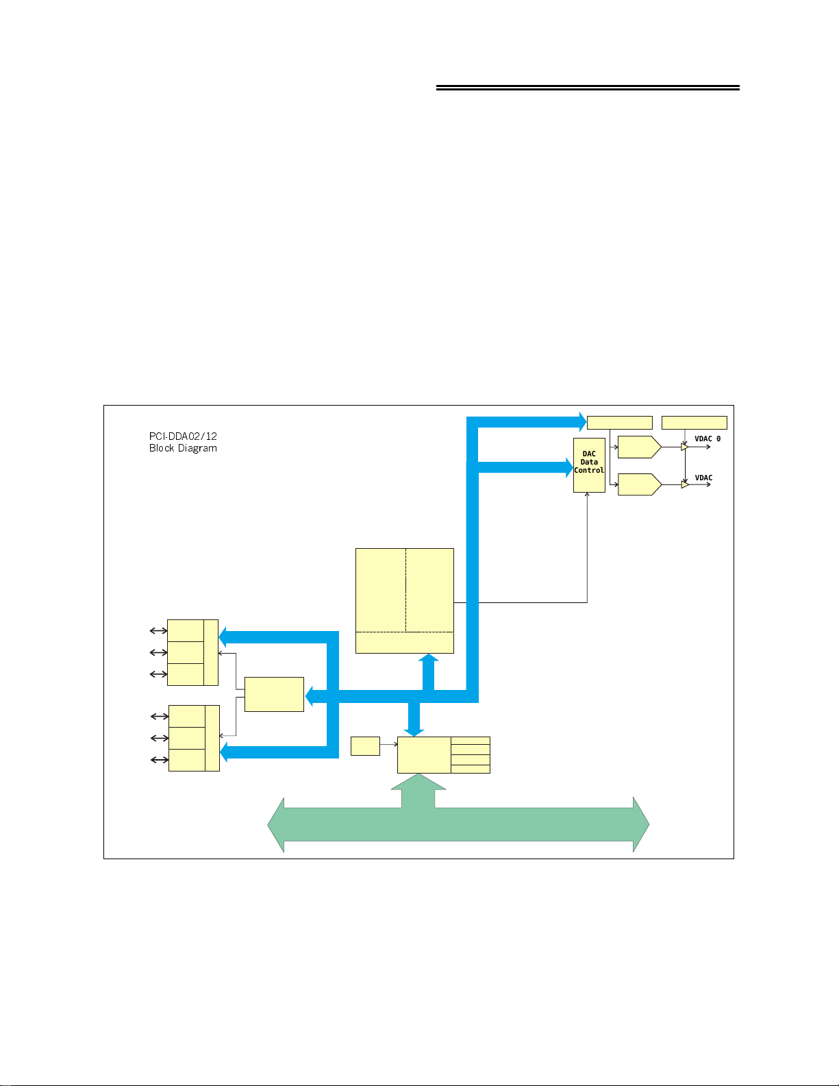
2.0 PRODUCT DESCRIPTION
The PCI-DDA0x/12 family comprises three PCI bus plug-in board models: PCI-DDA02/12, PCI-DDA04/12, and
PCI-DDA08/12, with 2, 4, and 8 12-bit analog output channels, respectively. In addition, each model has 48 digital
I/O lines.
The D/A converters can be independently configured for either bipolar or unipolar 2.5V, 5V, and 10V ranges. The
outputs may be updated individ ually or simultaneously. All calibration and range setti ngs are done through software.
The digital I/O ports are configured as two 8255 mode 0 emulations; A (8 bits), B (8 bits), C high (4 bits), and C low
(4 bits). The digital outputs are capable of sinking 64 ma and sourcing 15 ma utilizing standard "S" logic.
The PCI interface uses the PLX 9052 IC which is a low-cost slave-only device. The PCI interface for the analog
output is configured in a 16 bit, multiplexed address/data bus, I/O access mode. The PCI interface for the digital I/O
is configured in an 8 bit, multiplexed address/data bus, I/O access mode to be register compatible with the
PCI-DIOxxH and PCI-DIO48/CTR15 boards. For an idea of how the PCI-DDA0X/12 is logically constructed, refer
to the block diagram below according to your particular model.
Gain Autocal Offset Autocal
3&,''$
%ORFN 'LDJUDP
DAC
Data
Control
12-Bit
DAC0
12-Bit
DAC1
VDAC 0
VDAC 1
PA0 (7:0)
PB0 (7:0)
PC0 (7:0)
PA1 (7:0)
PB1 (7:0)
PC1 (7:0)
Digital I/O
Port A
Port B
Port C
Digital I/O
Port A
Port B
Port C
Control
Control
PAL
Digital I/O
Controller
Decode/Sta tu s
CONTROLLER
Calibration
Control
Decode/Status
33 MHz LOCAL BUS
Boot
EEPROM
PLD
Output
DAC
Control
BADR0
PCI
CONTROLLER
PCI BUS (5V, 32-BIT, 33MHZ)
BADR1
BADR2
BADR3
Page 3
Page 5
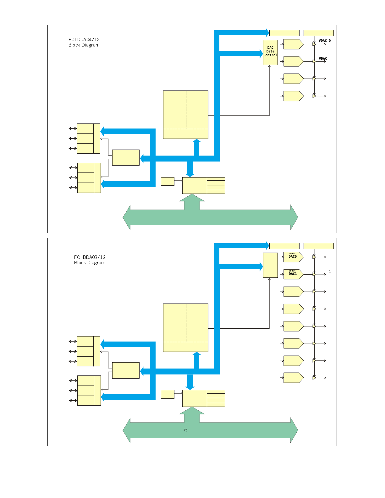
3&,''$
%ORFN 'LDJUDP
Gain Autocal Offset Autocal
12-Bit
DAC
Data
Control
DAC0
12-Bit
DAC1
VDAC 0
VDAC 1
PA0 (7:0)
PB0 (7:0)
PC0 (7:0)
PA1 (7:0)
PB1 (7:0)
PC1 (7:0)
Digital I/O
Port A
Port B
Control
Port C
Digital I/O
Port A
Port B
Control
Port C
3&,''$
%ORFN 'LDJUDP
PAL
Digital I/O
Controller
Decode/Sta tu s
CONTROLLER
Calibration
Control
Decode/Status
33 MHz LOCAL BUS
Boot
EEPROM
PLD
Output
DAC
Control
BADR0
PCI
CONTROLLER
BADR1
BADR2
BADR3
PCI BUS (5V, 32-BIT, 33MHZ)
12-Bit
DAC2
12-Bit
DAC3
Gain Autocal Offset Autocal
12-Bit
DAC
Data
Control
DAC0
12-Bit
DAC1
VDAC 2
VDAC 3
VDAC 0
VDAC 1
PA0 (7:0)
PB0 (7:0)
PC0 (7:0)
PA1 (7:0)
PB1 (7:0)
PC1 (7:0)
Digital I/O
Port A
Port B
Port C
Digital I/O
Port A
Port B
Port C
Control
Control
PAL
Digital I/O
Controller
Decode/Sta tu s
CONTROLLER
Calibration
Control
Decode/Status
33 MHz LOCAL BUS
Boot
EEPROM
PLD
Output
DAC
Control
BADR0
PCI
CONTROLLER
BADR1
BADR2
BADR3
PCI BUS (5V, 32-BIT, 33MHZ)
Page 4
12-Bit
DAC2
12-Bit
DAC3
12-Bit
DAC4
12-Bit
DAC5
12-Bit
DAC6
12-Bit
DAC7
VDAC 2
VDAC 3
VDAC 4
VDAC 5
VDAC 6
VDAC 7
Page 6

3.0 INSTALLATION
3.1 HARDWARE INSTALLATION
The PCI-DDA0x/12 products are completely plug and play. Simply follow the steps shown below to install your PCI
hardware.
1.
Turn your computer off, unplug it, open it up and insert the PCI board into any available PCI slot.
2.
Close your computer up, plug it back in and turn it on.
3.
Windows will automatically detect the board as it starts up. If the board's configuration file is already on the
system, it will load without user interaction. If the configuration file is not detected, you will be prompted to
insert the disk containing it. The required file is on the InstaCal or Universal Library disk you received with
your board. Simply insert the CD (or Disk 1 if your software is on floppy disk) into an appropriate drive and
click on
appear in the Device Manager under DAS Component.
If the file is not found on the first attempt, use the browse function to select the drive that contains the
InstaCAL or Universal Library disk, select the CBxx.INF file and then click on
CONTINUE
. The appropriate file should then be automatically loaded and the PCI board will
CONTINUE.
3.2 SOFTWARE INSTALLATION
3.2.1 INTRODUCTION
Insta
Cal is the installation, calibration and test software supplied with your data acquisition hardware. The complete
Insta
Cal package is also included with the Universal Library. If you have ordered the Universal Library, the Universal Library CD/disks install both the library and
the various pieces of compressed software. To install
the SETUP.EXE file contained on your CD, (or Disk 1 of the floppy disk set) and follow the on-screen instructions.
3.2.2 INSTALLATION OPTIONS
The Universal Library provides example programs for a wide var i ety of programming languages. If you are installing
the Universal Library, an "Installation Options" dialog box will allow you to select which languages' example
programs are loaded onto your computer. Select the desired example programs by checking the appropriate box(s).
3.2.3 FILE DEFAULT LOCATION
Insta
Cal will place all appropriate files in "C:CB" If you change this default location remember where the installed
files are placed as you may need to access them later.
3.2.4 INSTALLATION QUESTIONS
At the end of the installation process the installation wizard will ask a series of questions updating your startup files.
Unless you have knowledge to the contrary, simply accept the default (YES) when prompted. You will also be asked
if you would like to read an updated README file. If possible, please choose yes and take a look at the information
in the file. It will include the latest information regarding the software you are installing.
, WINDOWS
Insta
Cal. The installation will create all required files and unpack
Insta
Cal (and the Universal Library if applicable), simply run
95, 98 & NT
3.2.5 INSTALLATION COMPLETION
After the installation of
the system.
Insta
Cal is complete you should restart your computer to take advantage of changes made to
Page 5
Page 7

3.3 RUN INSTACAL
Run the InstaCal progr am in order to test your bo ard and co nfigure it for run-time use. By confi guring the boar d,
you add information to the configuration file, cb.cfg, that is used by the Universal Library and other third-party data
acquisition packages that use the Universal Library to access the board.
3.3.1 LAUNCHING InstaCAL
Launch InstaCal by going to your Start Menu then to Programs, then to ComputerBoards, and finally choosing Insta-
Cal. You may also launch the program by going to START >RUN and typing INSCAL32, or by finding the file
named "inscal32.exe" in your installation directory and double clicking it.
InstaCal will display a dialog box indicating the boards that have been detected in the system. If there are no other
boards currently installed by InstaCal, then the PCI-DDA0x/12 board will be assigned board number 0. Otherwise it
will be assigned the next available board number.
You can now view and change the b oa r d c o nfigur ati on b y clic king t he p ro p er ti es i co n o r se le cti ng the I nsta ll\Co nfigure menu.
3.3.2 TESTING THE INSTALLATION
After you have run the install program, it is time to test the installation. The following section describes the InstaCal
procedure to test that your board is properly installed.
With InstaCal running:
1. Select the board you just installed.
2. Select the "Test" function.
Follow the instructions provided to test for proper board operation.
3.4 DOS AND/OR WINDOWS 3.1
Most users are now installing PCI Bus boards in systems with 32-bit operating systems (e.g., Windo ws 95, 98 or
NT). The PCI-DDA0x/12 is not currently supported by the 16-bit library required to run under DOS or Windows
3.x.
Please contact us if your application is running under DOS or Windows 3.x.
Page 6
Page 8

4.0 CONNECTIONS
The PCI-DDA0x/12 uses a single 100-pin connector on the back plate of the board to bring out all required digital
and analog lines and grounds.
PLEASE NOTE: If you have a PCI-DDA08/12, all instructions in this manual apply. If you have a PCI-DDA04/12,
you should ignore all references to D/A channels 4 through 7; and if you have a PCI-DDA02/12, you should ignore
all references to D/A channels 2 through 7. In all other respects, the three models are identical.
4.1 CONNECTING EXTERNAL LINES
The 100-pin connector provides a far greater signal density
than the traditional 37 pin D type connector. The ideal means
for breaking out the 100 lines from the PCI-DDA0X/12 are a
combination of one C100-FF-X series cable
and either one CIO-TERM100 screw terminal board or a pair of CIO-MINI50 screw
terminal boards.
Each of the C100-FF-x cable series consists of a ribbon cable
that is terminated at one end with a 100 pin connector that
mates with the connector on the PCI-DDA0x/12 board. The
100-conductor ribbon cable splits into two 50 pin ribbon
cables which are terminated with standard 50 pin header
connectors that connect to the CIO-TERM100
or
CIO-MINI50 screw terminal boards. The C100-FF-x is available in lengths of 1, 2, 3, 4, 5, 10, 15, 20, 25, and 50 feet,
where x is the length in feet. For example, a two-foot model
is designated C100-FF-2.
Vout 0 1
Analog Ground
Analog Ground
Analog Ground
Analog Ground
Analog Ground
Analog Ground
Analog Ground
Analog Ground16
Digital Ground 50
2
Vout 1 3
4
Vout 2 5
6
Vout 3 7
8
Vout 4 9
10
Vout 5 11
12
Vout 6 13
14
Vout 7 15
NC
17
NC
18
NC
19
NC
20
NC
21
NC
22
NC
23
NC
24
NC
25
NC
26
NC
27
NC
28
NC
29
NC
30
NC
31
NC
32
NC
33
NC
34
NC
35
NC
36
NC
37
NC
38
NC
39
NC
40
NC
41
NC
42
NC
43
NC
44
NC
45
NC
46
NC
47
NC
48
NC 49
PCI-DDA0x/12 Connector Diagram
51 P2-A7
52 P2-A6
53 P2-A5
2-
54 P A4
2-
55 P A3
2-
56 P A2
2-
57 P A1
2-
58 P A0
2-
59 P B7
2-
60 P B6
2-
61 P B5
2-
62 P B4
2-
63 P B3
2-
64 P B2
2-
65 P B1
2-
66 P B0
2-
67 P C7
2-
68 P C6
2-
69 P C5
2-
70 P C4
2-
71 P C3
2-
72 P C2
2-
73 P C1
2-
74 P C0
-
75 P1A7
1-
76 P A6
1-
77 P A5
1-
78 P A4
1-
79 P A3
1-
80 P A2
1-
81 P A1
1-
82 P A0
1-
83 P B7
1-
84 P B6
1-
85 P B5
1-
86 P B4
1-
87 P B3
1-
88 P B2
1-
89 P B1
1-
90 P B0
1-
91 P C7
1-
92 P C6
1-
93 P C5
1-
94 P C4
1-
95 P C3
1-
96 P C2
1-
97 P C1
1-
98 P C0
99 +5V
100 Digital Ground
Page 7
Page 9

4.2 ANALOG CONNECTIONS
The analog output connections on the PCI-DDA0x/12 series are two-wire hookups, one end of which is the signal
labeled Voutx, with x being the channel number from 0 to 7 (PCI-DDA08/12), 0 to 3 (PCI-DDA04/12), and 0 to 1
(PCI-DDA02/12). The other end is the associated analog ground. In software you may select analog ranges of ±10V,
±5V, ±2.5V, 0 - 10V, 0 - 5V, and 0 - 2.5V. Each port may be reconfigured easily and quickly.
4.3 DIGITAL CONNECTIONS
The PCI-DDA0x/12 emulates two 82C55 chips, but offers much higher drive capability than the 82C55. The board
emulates only Mode 0 of the 82C55 (no strobed I/O or bi-directional I/O bits). The board is completely plug-andplay without any onboard user configurable switches or jumpers. The 48 CMOS/TTL compatible digital I/O lines are
configured in four banks of 8 and four banks of 4. Each group may be input or output.
All the digital outputs/inputs on the PCI-DDA0x/12 connector are TTL compatible. TTL is an electronics industry
term, short for Transistor Transistor Logic, which describes a standard for digital signals which are either at 0V or
5V. The binary logic inside the PC is all TTL or LSTTL (Low power Schottky TTL).
The outputs ar e cap a bl e o f sinking 6 4 mA or so urc ing 1 5 mA. All I/O is b r ought o ut to the 100-pin connector, which
also allows connection to the PC’s +5 Volt and Ground.
Keep in mind that unco nnected inputs flo at. If you are using a DIO bo ard for input, and have unconnecte d inputs,
ignore the data from those lines. In other words, if you connect bit A0 and not bit A1, do not be surprised if A1 stays
low, stays high or tracks A0. In the absence of a pull-up/down resistor, any input to a CIO-DIO which is unconnected is unspecified.
You do not have to connect all input lines, and unconnected lines will not affect the performance of connected lines.
Just make sure that you mask out any unconnected bits in software.
4.3.1 Pull Up and Pull Down Resistors
Whenever the board is powered on or reset, all ports are set to input mode. Inputs will typically float high, but will
not reliably supply enough output current to ensure that external d evices you have connected will “see” a logic 1.
Which way they float depends on the characteristics of the circuits connected and is unpredictable! If it is important
that your system go into a predetermined state on power up or reset, you need pull up/down resistors.
The pull-up resistor pulls the input to a high state (+5V) while its value of 2200 ohms requires only 2 ma of the 64
mA available from the output. A 2200 ohm pull-down resistor accomplishes the same task except that the line is
pulled low when the board is input mode (and uses only 2 mA of the available 15 mA output provided by the board).
The PCI-DDA0X boards are equipp ed with positions for pull-up/down resistors Single Inline Packages (SIPs). T he
positions are marked A, B and C and are located behind board’s I/O connector.
A 2.2K ohm, 9-resistor SIP is made of 9, 2.2K resistors all connected one side to a single common point and the
other, each to a pin protruding from the SIP. The common line to which all resistor are connected also protrudes
from the SIP. The common line is marked with a dot and is at one end of the SIP.
The SIP may be installed as pull-up or pull-down. At each SIP location, there are 10 holes in a line. One end of the
line is +5V, the other end is GND. They are so marked. The 8 holes in the middle are connected to the 8 lines of the
port.
Page 8
Page 10

5.0 PROGRAMMING & APPLICATIONS
Your PCI-DDA0x/12 is supported by the powerful Universal Library. We strongly recommend that
you take advantage of the Universal Library as your software interface. The complexity of the registers required for
automatic calibration combined with the dynamic allocation of addresses and internal resources makes the
PCI-DDA0x/12 series very challenging to program via direct register I/O operations. Direct I/O programming
should not be required.
5.1 PROGRAMMING LANGUAGES
The Universal Library provides complete access to the PCI-DDA0x/12 functions from a range of
Windows programming languages. If you are planning to write programs, or would like to run the example
programs for Visual Basic or any other language, please refer to the Universal Library manual.
The optional VIX Components package may greatly simplify your programming effort. VIX Components is a set of
programming tools based on a DLL interface to Windows languages. A set of VBX, OCX, and ActiveX interfaces
allows point and click construction of graphical displays, analysis and control structures. Please see a ComputerBoards product catalog or contact us for a complete description of VIX Components.
5.2 PACKAGED THIRD-PARTY APPLICATIONS PROGRAMS
In addition to DAS-Wizard, many packaged third-party application programs such as Labtech
Notebook and HP-VEE now have drivers for the PCI-DDA0x/12. If the package you own does not appear to have
drivers for the PCI-DDA0x/12 please fax or e-mail the package name and the revision number from the install disks.
We will research the package for you and advise how to obtain PCI-DDA0x/12 drivers.
Some application drivers that are included with Universal Library are not included with third-party application
packages. If you have purchased an application package directly from the software vendor, you may need to
purchase our Universal Library and drivers. Please contact us for more information on this topic.
Page 9
Page 11

6.0 Self-Calibration
The PCI-DDA0x/12 is shipped fully-calibrated from the factory with calibration coefficients stored in nonvolatile
RAM. When using the Universal Library, these calibration factors are read from nonvolatile RAM and are automatically written to the calibration DACS each time a different DAC range is specified. The user has the option to recalibrate with respect to the factory-measured voltage standards at any time by simply selecting the "Calibrate" option in
InstaCal. Instacal will calibrate all channels at all six ranges. Each channel takes less than a minute to calibrate.
6.1 CALIBRATION CONFIGURATION
The PCI-DDA0x/12 provides self-calibration of the analog source and measure systems thereby eliminating the need
for external equipment and user adjustments. Calibration factors are stored on the serial nonvolatile RAM.
The analog output circuits are calibrated for both gain and offset. Gain calibration of the analog outputs are
performed via DAC reference adjustments. Offset adjustments for the analog output are made in the output buffer
section. A block diagram of the PCI-DDA0x/12 series calibration circuitry is shown below.
VHULDO
*DLQ $GMXVW
&RDUVH
7ULP '$&V
)LQH
3UHFLVLRQ
9
VHULDO
3&,''$ &DOLEUDWLRQ %ORFN 'LDJUDP
2XWSXW '$&
AD78 37
9UHI
2IIVHW $GMXVW
VHULDO
&RDUVH
7ULP '$&V
)LQH
3URJUDPDEOH 9ROWDJH VRXUFH
0$;
5HIHUHQFH '$&
9RXW
3*$
;
2XWSXW
9ROWDJHV
6HWSRLQW 9ROWDJH
[
2XWSXW 9ROWDJH
3UHFLVLRQ
&RPSDUDWRU
&203
&RXQWHU
&/($5
Page 10
Page 12

6.2 "IN-SYSTEM" CALIBRATION
The PCI-DDA0x/12 is calibrated at the factory for the correct voltages at the I/O connector itself. For more precise
application of voltages at the "system end", we have provided a version of InstaCAL that allows you to calibrate the
board within your system, for correct voltages at your field connection. This calibration allows the user to remove
the effects of voltage drops caused by IR loss in the cable and connector for resistances up to 1 ohm. This calibration
will also allow the user to zero out errors in any external signal conditioning up to approximately ± 10 mV.
Please contact the factory for details regarding the use of this "in-system" calibration feature.
Page 11
Page 13

7.0 Register Description
We strongly urge users to take advantage of the Universal Library software package rather than attempt to write
register level software for the PCI-DDA0x/12 series. The register level programming information is provided as a
matter of completeness only. Register level programming of this or any other software calibrating PCI board is quite
complex and should only be attempted by highly experienced programmer.
7.1 REGISTER OVERVIEW
NOTE: please ignore references to D/A channels 4 through 7 on the PCI-DDA04/12, and references to channels 2
through 7 on the PCI-DDA02/12. Otherwise, the three boards are identical.
PCI-DDA0x/12 operation registers are mapped into I/O space. Unlike ISA bus designs, this board has several base
addresses, each corresponding to a reserved block of addresses in I/O space.
Of the six Base Address Regions (BADR) available per the PCI 2.1 specification, four are implemented in this
design and are summarized as follows.
OperationsFunctionI/O Region
32-bit DOUBLE WORDPCI memory mapped configuration registersBADR0
32-bit DOUBLE WORDPCI I/O mapped configuration registersBADR1
8-bit BYTEDigital I/O registersBADR2
16-bit WORDDAC registersBADR3
BADR0 and BADR1 are used for PCI configuration and should be used only by experienced programmers familiar
with the PCI interface. BADR2 is an 8-bit data/address bus for compatibility with our other digital I/O PCI cards.
BADR3 is a 16-bit data/address bus for software ease when writing to the 12-bit DACs.
7.2 BADR2
Write FunctionRead FunctionRegister
Output Port 1A DataInput Port 1A DataBADR2 + 0
Output Port 1B DataInput Port 1B DataBADR2 + 1
Output Port 1C DataInput Port 1C DataBADR2 + 2
Control Register 1Control register readback 1BADR2 + 3
Output Port 2A DataInput Port 2A DataBADR2 + 4
Output Port 2B DataInput Port 2B DataBADR2 + 5
Output Port 2C DataInput Port 2C DataBADR2 + 6
Control Register 2Control register readback 2BADR2 + 7
The Digital I/O ports simulate the 8255 Mode 0 function
PORT 1A DATA
BADR2 + 0hex
READ/WRITE
.
01234567
A0A1A2A3A4A5A6A7
Page 12
Page 14

PORT 1B DATA
BADR2 + 1hex
READ/WRITE
01234567
B0B1B2B3B4B5B6B7
PORT 1C DATA
BADR2 + 02hex
READ/WRITE
01234567
CL0CL1CL2CL3CH0CH1CH2CH3
CONTROL REGISTER 1
BADR2 + 03hex
READ/WRITE
01234567
D0D1-D3D4---
The operating mode of the Digital I/O port is set to Mode 0. The control register therefore is used to enable the ports
for input/output to the connector. For example, to set all ports to output, write the value 0hex to BADR2 + 3. To set
all ports to input, write the value 1Bhex to Base + 3. T he user is able to read the current state of the output por t by
simply reading that port when set to be output. D7, D6, D5, and D2 are ‘don’t care’. ‘CU’ is PORT C upper nibble,
‘CL’ is PORT C lower nibble.
Table 1.0
DIO PortValuesProgramming Codes
CUBADecHexD0D1D3D4
CL
OUTOUTOUTOUT000000
INOUTOUTOUT111000
OUTOUTINOUT220100
INOUTINOUT331100
OUTINOUTOUT880010
ININOUTOUT991010
OUTININOUT10A0110
INININOUT11B1110
OUTOUTOUTIN16100001
INOUTOUTIN17111001
OUTOUTININ18120101
INOUTININ19131101
OUTINOUTIN24180011
ININOUTIN25191011
OUTINININ261A0111
ININININ271B1111
Page 13
Page 15

PORT 2A DATA
BADR2 + 04hex
READ/WRITE
PORT 2B DATA
BADR2 + 05hex
READ/WRITE
PORT 2C DATA
BADR2 + 06hex
READ/WRITE
01234567
A0A1A2A3A4A5A6A7
01234567
B0B1B2B3B4B5B6B7
01234567
CL0CL1CL2CL3CH0CH1CH2CH3
CONTROL REGISTER 2
BADR2 + 07hex
READ/WRITE
See BADR2 + 03hex and TABLE 1.0 for full description of the Control Register.
7.3 BADR3
WRITE FUNCTIONREAD FUNCTIONREGISTER
D/A Control RegisterInitiate a simultaneous updateBADR3 + 0
reservedBADR3 + 2h
D/A Calibration Register 1 D/A Calibration Register 1 DataBADR3 + 4h
D/A Calibration Register 2BADR3 + 6h
D/A 0 DATA BADR3 + 8h
D/A 1 DATABADR3 + Ah
D/A 2 DATABADR3 + Ch
D/A 3 DATABADR3 + Eh
D/A 4 DATABADR3 + 10h
D/A 5 DATABADR3 + 12h
D/A 6 DATABADR3 + 14h
D/A 7 DATABADR3 + 16h
01234567
D0D1-D3D4---
Page 14
Page 16

D/A CONTROL REGISTER
BADR3 + 0hex
WRITE
SU
This bit enables simultaneous update for the DAC pair specified by D2 and D1 (see table below). Setting the simultaneous update bit inhibits updating the DAC output until a simultaneous update is initiated (see READ below). The
DACs are paired as follows; DACs 0 and 1, DACs 2 and 3, DACs 4 and 5, and DACs 6 and 7. Setting simultaneous
update for either DAC in the pair will set it for both.
The power on status of this bit is 0
EN
This bit enables the DAC specified by D2, D1, D0.
The power on status of this bit is 0. A disabled DAC is held at 0v.
D[2:0]
These bits specify the DAC that is being configured.
0123456789101112131415
SUEND0D1D2XR0R1R2XXXXXXX
0 = Simultaneous update disabled
1 = Simultaneous update enabled
0 = DAC disabled
1 = DAC enabled
R[2:0]
These bits select the gain/range for the DAC specified by D2, D1, and D0.
The power on setting is Bipolar 2.5V.
DAC ChannelD0D1D2
0000
1100
2010
3110
4001
5101
6011
7111
LSB SizeRANGER0R1R2
1.22mVBipolar 2.5VX00
2.44mVBipolar 5V010
4.88mVBipolar 10V110
611uVUnipolar 2.5VX01
1.22mVUnipolar 5V011
2.44mVUnipolar 10V111
Page 15
Page 17

READ
Reading this register initiates a simultaneous update for all DACs.
D/A CALIBRATION REGISTER 1
BADR3 + 4hex
WRITE
01234567
SDIMA0MA1MA2XXXX
SDI
This is the serial data in bit for the calibration EEPROM, the 16-bit reference DAC, and the 8-bit trim DACs.
Writing to this register will automatically generate the correct serial clock.
NOTE: You must preserve the status of MA2:MA0 when adjusting the offset and gain calibration DACs.
MA[2:0]
These bits select the DAC to be calibrated
DAC ChannelMA0MA1MA2
0000
1100
2010
3110
4001
5101
6011
7111
READ
01234567
D0D1D2D3D4OVERFLOWCOMPSDO
D[4:0]
These bits are the output of the 5 bit calibration counter. D0 is the LSB. Each time you initiate a read, the counter is
first cleared and then gated (allowed to count) for a fixed period. This ensures that all count periods are identical.
OVERFLOW
This bit indicates that a 5-bit calibration counter overflow.
0 = no counter overflow
1 = counter overflow
Page 16
Page 18

COMP
This bit comes from the output of the calibration comparitor.
0 = DAC voltage is greater than the calibration reference voltage
1 = DAC voltage is less than the calibration reference voltage
SDO
This is the serial data out bit for the calibration EEPROM. Reading this register will automatically generate the
correct serial clock.
D/A CALIBRATION REGISTER 2
BADR3 + 6hex
WRITE ONLY
01234567
SEL_EEPROMSEL_542SEL8800_01SEL8800_23SEL8800_45SEL8800_671X
SEL_EEPROM
This bit is the chip select for the calibration EEPROM. It is active high and should be initialized to 0. Make sure that
none of the DACs discussed below are enabled at the same time as the EEPROM because they share common serial
data and clock lines. The calibration EEPROM is the NM93C56 which is divided into 128 16-bit words. The
memory map is listed in the tables below. Data is clocked in and out on the rising edge of the serial clock. The
decoding logic on the board drives the serial clock automatically so no additional programming is required. You
must send a WREN (write enable) command to the device before trying to write to it.
DescriptionAddress
+9.99756V Reference DAC 16-bit word 00h
+9.99512V Reference DAC 16-bit word 01h
+4.99878V Reference DAC 16-bit word 02h
+4.99756V Reference DAC 16-bit word03h
+2.49939V Reference DAC 16-bit word04h
+2.49878V Reference DAC 16-bit word05h
0V Reference DAC 16-bit word06h
Table 2.0 EEPROM Memory Map for the Reference DAC
Page 17
Page 19

Lower ByteUpper ByteAddress
Bipolar 10V Trim DAC0 Fine OffsetBipolar 10V Trim DAC0 Coarse Offset07h
Bipolar 10V Trim DAC0 Fine GainBipolar 10V Trim DAC0 Coarse Gain08h
Bipolar 5V Trim DAC0 Fine OffsetBipolar 5V Trim DAC0 Coarse Offset09h
Bipolar 5V Trim DAC0 Fine GainBipolar 5V Trim DAC0 Coarse Gain0Ah
Bipolar 2.5V Trim DAC0 Fine OffsetBipolar 2.5V Trim DAC0 Coarse Offset0Bh
Bipolar 2.5V Trim DAC0 Fine GainBipolar 2.5V Trim DAC0 Coarse Gain0Ch
Unipolar 10V Trim DAC0 Fine OffsetUnipolar 10V Trim DAC0 Coarse Offset0Dh
Unipolar 10V Trim DAC0 Fine GainUnipolar 10V Trim DAC0 Coarse Gain0Eh
Unipolar 5V Trim DAC0 Fine OffsetUnipolar 5V Trim DAC0 Coarse Offset0Fh
Unipolar 5V Trim DAC0 Fine GainUnipolar 5V Trim DAC0 Coarse Gain10h
Unipolar 2.5V Trim DAC0 Fine OffsetUnipolar 2.5V Trim DAC0 Coarse Offset11h
Unipolar 2.5V Trim DAC0 Fine GainUnipolar 2.5V Trim DAC0 Coarse Gain12h
Bipolar 10V Trim DAC1 Fine OffsetBipolar 10V Trim DAC1 Coarse Offset13h
Bipolar 10V Trim DAC1 Fine GainBipolar 10V Trim DAC1 Coarse Gain14h
Bipolar 5V Trim DAC1 Fine OffsetBipolar 5V Trim DAC1 Coarse Offset15h
Bipolar 5V Trim DAC1 Fine GainBipolar 5V Trim DAC1 Coarse Gain16h
Bipolar 2.5V Trim DAC1 Fine OffsetBipolar 2.5V Trim DAC1 Coarse Offset17h
Bipolar 2.5V Trim DAC1 Fine GainBipolar 2.5V Trim DAC1 Coarse Gain18h
Unipolar 10V Trim DAC1 Fine OffsetUnipolar 10V Trim DAC1 Coarse Offset19h
Unipolar 10V Trim DAC1 Fine GainUnipolar 10V Trim DAC1 Coarse Gain1Ah
Unipolar 5V Trim DAC1 Fine OffsetUnipolar 5V Trim DAC1 Coarse Offset1Bh
Unipolar 5V Trim DAC1 Fine GainUnipolar 5V Trim DAC1 Coarse Gain1Ch
Unipolar 2.5V Trim DAC1 Fine OffsetUnipolar 2.5V Trim DAC1 Coarse Offset1Dh
Unipolar 2.5V Trim DAC1 Fine GainUnipolar 2.5V Trim DAC1 Coarse Gain1Eh
Bipolar 10V Trim DAC2 Fine OffsetBipolar 10V Trim DAC2 Coarse Offset1Fh
Bipolar 10V Trim DAC2 Fine GainBipolar 10V Trim DAC2 Coarse Gain20h
Bipolar 5V Trim DAC2 Fine OffsetBipolar 5V Trim DAC2 Coarse Offset21h
Bipolar 5V Trim DAC2 Fine GainBipolar 5V Trim DAC2 Coarse Gain22h
Bipolar 2.5V Trim DAC2 Fine OffsetBipolar 2.5V Trim DAC2 Coarse Offset23h
Bipolar 2.5V Trim DAC2 Fine GainBipolar 2.5V Trim DAC2 Coarse Gain24h
Unipolar 10V Trim DAC2 Fine OffsetUnipolar 10V Trim DAC2 Coarse Offset25h
Unipolar 10V Trim DAC2 Fine GainUnipolar 10V Trim DAC2 Coarse Gain26h
Unipolar 5V Trim DAC2 Fine OffsetUnipolar 5V Trim DAC2 Coarse Offset27h
Unipolar 5V Trim DAC2 Fine GainUnipolar 5V Trim DAC2 Coarse Gain28h
Unipolar 2.5V Trim DAC2 Fine OffsetUnipolar 2.5V Trim DAC2 Coarse Offset29h
Unipolar 2.5V Trim DAC2 Fine GainUnipolar 2.5V Trim DAC2 Coarse Gain2Ah
Table 3.0 Calibration EEPROM Memory Map for Trim DACs
Page 18
Page 20

Lower ByteUpper ByteAddress
Bipolar 10V Trim DAC3 Fine OffsetBipolar 10V Trim DAC3 Coarse Offset2Bh
Bipolar 10V Trim DAC3 Fine GainBipolar 10V Trim DAC3 Coarse Gain2Ch
Bipolar 5V Trim DAC3 Fine OffsetBipolar 5V Trim DAC3 Coarse Offset2Dh
Bipolar 5V Trim DAC3 Fine GainBipolar 5V Trim DAC3 Coarse Gain2Eh
Bipolar 2.5V Trim DAC3 Fine OffsetBipolar 2.5V Trim DAC3 Coarse Offset2Fh
Bipolar 2.5V Trim DAC3 Fine GainBipolar 2.5V Trim DAC3 Coarse Gain30h
Unipolar 10V Trim DAC3 Fine OffsetUnipolar 10V Trim DAC3 Coarse Offset31h
Unipolar 10V Trim DAC3 Fine GainUnipolar 10V Trim DAC3 Coarse Gain32h
Unipolar 5V Trim DAC3 Fine OffsetUnipolar 5V Trim DAC3 Coarse Offset33h
Unipolar 5V Trim DAC3 Fine GainUnipolar 5V Trim DAC3 Coarse Gain34h
Unipolar 2.5V Trim DAC3 Fine OffsetUnipolar 2.5V Trim DAC3 Coarse Offset35h
Unipolar 2.5V Trim DAC3 Fine GainUnipolar 2.5V Trim DAC3 Coarse Gain36h
Bipolar 10V Trim DAC4 Fine OffsetBipolar 10V Trim DAC4 Coarse Offset37h
Bipolar 10V Trim DAC4 Fine GainBipolar 10V Trim DAC4 Coarse Gain38h
Bipolar 5V Trim DAC4 Fine OffsetBipolar 5V Trim DAC4 Coarse Offset39h
Bipolar 5V Trim DAC4 Fine GainBipolar 5V Trim DAC4 Coarse Gain3Ah
Bipolar 2.5V Trim DAC4 Fine OffsetBipolar 2.5V Trim DAC4 Coarse Offset3Bh
Bipolar 2.5V Trim DAC4 Fine GainBipolar 2.5V Trim DAC4 Coarse Gain3Ch
Unipolar 10V Trim DAC4 Fine OffsetUnipolar 10V Trim DAC4 Coarse Offset3Dh
Unipolar 10V Trim DAC4 Fine GainUnipolar 10V Trim DAC4 Coarse Gain3Eh
Unipolar 5V Trim DAC4 Fine OffsetUnipolar 5V Trim DAC4 Coarse Offset3Fh
Unipolar 5V Trim DAC4 Fine GainUnipolar 5V Trim DAC4 Coarse Gain40h
Unipolar 2.5V Trim DAC4 Fine OffsetUnipolar 2.5V Trim DAC4 Coarse Offset41h
Unipolar 2.5V Trim DAC4 Fine GainUnipolar 2.5V Trim DAC4 Coarse Gain42h
Bipolar 10V Trim DAC5 Fine OffsetBipolar 10V Trim DAC5 Coarse Offset43h
Bipolar 10V Trim DAC5 Fine GainBipolar 10V Trim DAC5 Coarse Gain44h
Bipolar 5V Trim DAC5 Fine OffsetBipolar 5V Trim DAC5 Coarse Offset45h
Bipolar 5V Trim DAC5 Fine GainBipolar 5V Trim DAC5 Coarse Gain46h
Bipolar 2.5V Trim DAC5 Fine OffsetBipolar 2.5V Trim DAC5 Coarse Offset47h
Bipolar 2.5V Trim DAC5 Fine GainBipolar 2.5V Trim DAC5 Coarse Gain48h
Unipolar 10V Trim DAC5 Fine OffsetUnipolar 10V Trim DAC5 Coarse Offset49h
Unipolar 10V Trim DAC5 Fine GainUnipolar 10V Trim DAC5 Coarse Gain4Ah
Unipolar 5V Trim DAC5 Fine OffsetUnipolar 5V Trim DAC5 Coarse Offset4Bh
Unipolar 5V Trim DAC5 Fine GainUnipolar 5V Trim DAC5 Coarse Gain4Ch
Unipolar 2.5V Trim DAC5 Fine OffsetUnipolar 2.5V Trim DAC5 Coarse Offset4Dh
Unipolar 2.5V Trim DAC5 Fine GainUnipolar 2.5V Trim DAC5 Coarse Gain4Eh
Table 3.0 (cont.) Calibration EEPROM Memory Map for Trim DACs
Page 19
Page 21

Lower ByteUpper ByteAddress
Bipolar 10V Trim DAC6 Fine OffsetBipolar 10V Trim DAC6 Coarse Offset4Fh
Bipolar 10V Trim DAC6 Fine GainBipolar 10V Trim DAC6 Coarse Gain50h
Bipolar 5V Trim DAC6 Fine OffsetBipolar 5V Trim DAC6 Coarse Offset51h
Bipolar 5V Trim DAC6 Fine GainBipolar 5V Trim DAC6 Coarse Gain52h
Bipolar 2.5V Trim DAC6 Fine OffsetBipolar 2.5V Trim DAC6 Coarse Offset53h
Bipolar 2.5V Trim DAC6 Fine GainBipolar 2.5V Trim DAC6 Coarse Gain54h
Unipolar 10V Trim DAC6 Fine OffsetUnipolar 10V Trim DAC6 Coarse Offset55h
Unipolar 10V Trim DAC6 Fine GainUnipolar 10V Trim DAC6 Coarse Gain56h
Unipolar 5V Trim DAC6 Fine OffsetUnipolar 5V Trim DAC6 Coarse Offset57h
Unipolar 5V Trim DAC6 Fine GainUnipolar 5V Trim DAC6 Coarse Gain58h
Unipolar 2.5V Trim DAC6 Fine OffsetUnipolar 2.5V Trim DAC6 Coarse Offset59h
Unipolar 2.5V Trim DAC6 Fine GainUnipolar 2.5V Trim DAC6 Coarse Gain5Ah
Bipolar 10V Trim DAC7 Fine OffsetBipolar 10V Trim DAC7 Coarse Offset5Bh
Bipolar 10V Trim DAC7 Fine GainBipolar 10V Trim DAC7 Coarse Gain5Ch
Bipolar 5V Trim DAC7 Fine OffsetBipolar 5V Trim DAC7 Coarse Offset5Dh
Bipolar 5V Trim DAC7 Fine GainBipolar 5V Trim DAC7 Coarse Gain5Eh
Bipolar 2.5V Trim DAC7 Fine OffsetBipolar 2.5V Trim DAC7 Coarse Offset5Fh
Bipolar 2.5V Trim DAC7 Fine GainBipolar 2.5V Trim DAC7 Coarse Gain60h
Unipolar 10V Trim DAC7 Fine OffsetUnipolar 10V Trim DAC7 Coarse Offset61h
Unipolar 10V Trim DAC7 Fine GainUnipolar 10V Trim DAC7 Coarse Gain62h
Unipolar 5V Trim DAC7 Fine OffsetUnipolar 5V Trim DAC7 Coarse Offset63h
Unipolar 5V Trim DAC7 Fine GainUnipolar 5V Trim DAC7 Coarse Gain64h
Unipolar 2.5V Trim DAC7 Fine OffsetUnipolar 2.5V Trim DAC7 Coarse Offset65h
Unipolar 2.5V Trim DAC7 Fine GainUnipolar 2.5V Trim DAC7 Coarse Gain66h
Table 3.0 (cont.) Calibration EEPROM Memory Map for Trim DACs
Page 20
Page 22

Read word programming sequence
1.
Select the EEPROM by writing 127 (7Fh) to BADR3 + 6hex (D/A CALIBRATION REGISTER 2).
2.
Write 01h to bit 0 of BADR3 + 4hex (D/A CALIBRATION REGISTER 1).
3.
Write 01h to bit 0 of BADR3 + 4hex (D/A CALIBRATION REGISTER 1).
4.
Write 00h to bit 0 of BADR3 + 4hex (D/A CALIBRATION REGISTER 1).
5.
Write address bit 7 to bit 0 of BADR3 + 4hex (D/A CALIBRATION REGISTER 1).
6.
Write address bit 6 to bit 0 of BADR3 + 4hex (D/A CALIBRATION REGISTER 1).
7.
Write address bit 5 to bit 0 of BADR3 + 4hex (D/A CALIBRATION REGISTER 1).
8.
Write address bit 4 to bit 0 of BADR3 + 4hex (D/A CALIBRATION REGISTER 1).
9.
Write address bit 3 to bit 0 of BADR3 + 4hex (D/A CALIBRATION REGISTER 1).
10.
Write address bit 2 to bit 0 of BADR3 + 4hex (D/A CALIBRATION REGISTER 1).
11.
Write address bit 1 to bit 0 of BADR3 + 4hex (D/A CALIBRATION REGISTER 1).
12.
Write address bit 0 to bit 0 of BADR3 + 4hex (D/A CALIBRATION REGISTER 1).
13.
Read BADR3 + 4hex (D/A CALIBRATION REGISTER 1). Data bit 15 will be in register bit 7.
14.
Read BADR3 + 4hex (D/A CALIBRATION REGISTER 1). Data bit 14 will be in register bit 7.
15.
Read BADR3 + 4hex (D/A CALIBRATION REGISTER 1). Data bit 13 will be in register bit 7.
16.
Read BADR3 + 4hex (D/A CALIBRATION REGISTER 1). Data bit 12 will be in register bit 7.
17.
Read BADR3 + 4hex (D/A CALIBRATION REGISTER 1). Data bit 11 will be in register bit 7.
18.
Read BADR3 + 4hex (D/A CALIBRATION REGISTER 1). Data bit 10 will be in register bit 7.
19.
Read BADR3 + 4hex (D/A CALIBRATION REGISTER 1). Data bit 9 will be in register bit 7.
20.
Read BADR3 + 4hex (D/A CALIBRATION REGISTER 1). Data bit 8 will be in register bit 7.
21.
Read BADR3 + 4hex (D/A CALIBRATION REGISTER 1). Data bit 7 will be in register bit 7.
22.
Read BADR3 + 4hex (D/A CALIBRATION REGISTER 1). Data bit 6 will be in register bit 7.
23.
Read BADR3 + 4hex (D/A CALIBRATION REGISTER 1). Data bit 5 will be in register bit 7.
24.
Read BADR3 + 4hex (D/A CALIBRATION REGISTER 1). Data bit 4 will be in register bit 7.
25.
Read BADR3 + 4hex (D/A CALIBRATION REGISTER 1). Data bit 3 will be in register bit 7.
26.
Read BADR3 + 4hex (D/A CALIBRATION REGISTER 1). Data bit 2 will be in register bit 7.
27.
Read BADR3 + 4hex (D/A CALIBRATION REGISTER 1). Data bit 1 will be in register bit 7.
28.
Read BADR3 + 4hex (D/A CALIBRATION REGISTER 1). Data bit 0 will be in register bit 7.
29.
Deselect the EEPROM by writing 127 (7Eh) to BADR3 + 6hex (D/A CALIBRATION REGISTER 2).
Page 21
Page 23

Write enable programming sequence
1.
Select the EEPROM by writing 127 (7Fh) to BADR3 + 6hex (D/A CALIBRATION REGISTER 2).
2.
Write 01h to bit 0 of BADR3 + 4hex (D/A CALIBRATION REGISTER 1).
3.
Write 00h to bit 0 of BADR1 + 4hex (D/A CALIBRATION REGISTER 1).
4.
Write 00h to bit 0 of BADR3 + 4hex (D/A CALIBRATION REGISTER 1).
5.
Write 01h to bit 0 of BADR3 + 4hex (D/A CALIBRATION REGISTER 1).
6.
Write 01h to bit 0 of BADR3 + 4hex (D/A CALIBRATION REGISTER 1).
7.
Write 01h to bit 0 of BADR3 + 4hex (D/A CALIBRATION REGISTER 1).
8.
Write 01h to bit 0 of BADR3 + 4hex (D/A CALIBRATION REGISTER 1).
9.
Write 01h to bit 0 of BADR3 + 4hex (D/A CALIBRATION REGISTER 1).
10.
Write 01h to bit 0 of BADR3 + 4hex (D/A CALIBRATION REGISTER 1).
11.
Write 01h to bit 0 of BADR3 + 4hex (D/A CALIBRATION REGISTER 1).
12.
Write 01h to bit 0 of BADR3 + 4hex (D/A CALIBRATION REGISTER 1).
13.
Deselect the EEPROM by writing 126 (7Eh) to BADR3 + 6hex (D/A CALIBRATION REGISTER 2).
Write word programming sequence
1.
Select the EEPROM by writing 127 (7Fh) to BADR3 + 6hex (D/A CALIBRATION REGISTER 2).
2.
Write 01h to bit 0 of BADR3 + 4hex (D/A CALIBRATION REGISTER 1).
3.
Write 00h to bit 0 of BADR3 + 4hex (D/A CALIBRATION REGISTER 1).
4.
Write 01h to bit 0 of BADR3 + 4hex (D/A CALIBRATION REGISTER 1).
5.
Write address bit 7 to bit 0 of BADR3 + 4hex (D/A CALIBRATION REGISTER 1).
6.
Write address bit 6 to bit 0 of BADR3 + 4hex (D/A CALIBRATION REGISTER 1).
7.
Write address bit 5 to bit 0 of BADR3 + 4hex (D/A CALIBRATION REGISTER 1).
8.
Write address bit 4 to bit 0 of BADR3 + 4hex (D/A CALIBRATION REGISTER 1).
9.
Write address bit 3 to bit 0 of BADR3 + 4hex (D/A CALIBRATION REGISTER 1).
10.
Write address bit 2 to bit 0 of BADR3 + 4hex (D/A CALIBRATION REGISTER 1).
11.
Write address bit 1 to bit 0 of BADR3 + 4hex (D/A CALIBRATION REGISTER 1).
12.
Write address bit 0 to bit 0 of BADR3 + 4hex (D/A CALIBRATION REGISTER 1).
13.
Write data bit 15 to bit 0 of BADR3 + 4hex (D/A CALIBRATION REGISTER 1).
14.
Write data bit 14 to bit 0 of BADR3 + 4hex (D/A CALIBRATION REGISTER 1).
15.
Write data bit 13 to bit 0 of BADR3 + 4hex (D/A CALIBRATION REGISTER 1).
Page 22
Page 24

16.
Write data bit 12 to bit 0 of BADR3 + 4hex (D/A CALIBRATION REGISTER 1).
17.
Write data bit 11 to bit 0 of BADR3 + 4hex (D/A CALIBRATION REGISTER 1).
18.
Write data bit 10 to bit 0 of BADR3 + 4hex (D/A CALIBRATION REGISTER 1).
19.
Write data bit 9 to bit 0 of BADR3 + 4hex (D/A CALIBRATION REGISTER 1).
20.
Write data bit 8 to bit 0 of BADR3 + 4hex (D/A CALIBRATION REGISTER 1).
21.
Write data bit 7 to bit 0 of BADR3 + 4hex (D/A CALIBRATION REGISTER 1).
22.
Write data bit 6 to bit 0 of BADR3 + 4hex (D/A CALIBRATION REGISTER 1).
23.
Write data bit 5 to bit 0 of BADR3 + 4hex (D/A CALIBRATION REGISTER 1).
24.
Write data bit 4 to bit 0 of BADR3 + 4hex (D/A CALIBRATION REGISTER 1).
25.
Write data bit 3 to bit 0 of BADR3 + 4hex (D/A CALIBRATION REGISTER 1).
26.
Write data bit 2 to bit 0 of BADR3 + 4hex (D/A CALIBRATION REGISTER 1).
27.
Write data bit 1 to bit 0 of BADR3 + 4hex (D/A CALIBRATION REGISTER 1).
28.
Write data bit 0 to bit 0 of BADR3 + 4hex (D/A CALIBRATION REGISTER 1).
29.
Deselect the EEPROM by writing 126 (7Eh) to BADR3 + 6hex (D/A CALIBRATION REGISTER 2).
30.
Delay 10 ms before selecting the EEPROM again.
SEL_542
This bit is the chip select for the 16 bit serial reference DAC.
sure that the EEPROM and the trim DACs are not enabled at the same time as the reference DAC because they share
common serial data and clock lines. The reference DAC is the MAX542 which is a 16-bit voltage output serial
DAC. The reference voltage range is +/-10V (created by using the MAX542 in bipolar mode and amplifying its
output with a x4 precision amplifier.) Data is clocked in and out on the rising edge of the serial clock. The decoding
logic on the board drives the serial clock automatically so no additional programming is required. The calibration
values for the reference DAC have been set at the factory and can be read from the EEPROM, see table 1 above.
It is active low and should be initialized t o 1 .
Make
Write word programming sequence
1.
Select the MAX542 by writing 124 (7Ch) to BADR3 + 6hex (D/A CALIBRATION REGISTER 2).
2.
Write data bit 15 to bit 0 of BADR3 + 4hex (D/A CALIBRATION REGISTER 1).
3.
Write data bit 14 to bit 0 of BADR3 + 4hex (D/A CALIBRATION REGISTER 1).
4.
Write data bit 13 to bit 0 of BADR3 + 4hex (D/A CALIBRATION REGISTER 1).
5.
Write data bit 12 to bit 0 of BADR3 + 4hex (D/A CALIBRATION REGISTER 1).
6.
Write data bit 11 to bit 0 of BADR3 + 4hex (D/A CALIBRATION REGISTER 1).
7.
Write data bit 10 to bit 0 of BADR3 + 4hex (D/A CALIBRATION REGISTER 1).
8.
Write data bit 9 to bit 0 of BADR3 + 4hex (D/A CALIBRATION REGISTER 1).
9.
Write data bit 8 to bit 0 of BADR3 + 4hex (D/A CALIBRATION REGISTER 1).
Page 23
Page 25

10.
Write data bit 7 to bit 0 of BADR3 + 4hex (D/A CALIBRATION REGISTER 1).
11.
Write data bit 6 to bit 0 of BADR3 + 4hex (D/A CALIBRATION REGISTER 1).
12.
Write data bit 5 to bit 0 of BADR3 + 4hex (D/A CALIBRATION REGISTER 1).
13.
Write data bit 4 to bit 0 of BADR3 + 4hex (D/A CALIBRATION REGISTER 1).
14.
Write data bit 3 to bit 0 of BADR3 + 4hex (D/A CALIBRATION REGISTER 1).
15.
Write data bit 2 to bit 0 of BADR3 + 4hex (D/A CALIBRATION REGISTER 1).
16.
Write data bit 1 to bit 0 of BADR3 + 4hex (D/A CALIBRATION REGISTER 1).
17.
Write data bit 0 to bit 0 of BADR3 + 4hex (D/A CALIBRATION REGISTER 1).
18.
Deselect the MAX542 by writing 126 (7Eh) to BADR3 + 6hex (D/A CALIBRATION REGISTER 2).
SEL8800_xy
These bits are the load_dac controls for the offset and gain Trim DACs, DAC8800s, which are 8 channel, 8-bit,
voltage output, serial DACs.
and the reference DAC discussed above are not enabled at the same time as the trim DACs because they share
common serial data and clock lines. Each DAC8800 is used for the calibration of two output DACs, xy. For
example, bit 2, SEL8800_01, is the chip select for the DAC8800 that calibrates output DACs 0 and 1. There are
course and fine adjust DAC outputs for both offset and gain error calibration (see table below). Data is clocked in
on the rising edge of the serial clock. The decoding logic on the board drives the serial clock automatically so no
additional programming is required.
They are active low and should be initia lized to 1.
Make sure that the EEPROM
A0A1A2Cal FunctionTrim DAC Channel
000DACx Fine Gain0
100DACx Coarse Gain1
010DACx Coarse Offset2
110DACx Fine Offset3
001DACy Fine Gain4
101DACy Coarse Gain5
011DACy Coarse Offset6
111DACy Fine Offset7
Write byte programming sequence
1.
Write address bit A2 to bit 0 of BADR3 + 4hex (D/A CALIBRATION REGISTER 1). See table
above for correct value of A2.
2.
Write address bit A1 to bit 0 of BADR3 + 4hex (D/A CALIBRATION REGISTER 1). See table
above for correct value of A1.
3.
Write address bit A0 to bit 0 of BADR3 + 4hex (D/A CALIBRATION REGISTER 1). See table
above for correct value of A0.
4.
Write data bit 7 to bit 0 of BADR3 + 4hex (D/A CALIBRATION REGISTER 1).
5.
Write data bit 6 to bit 0 of BADR3 + 4hex (D/A CALIBRATION REGISTER 1).
6.
Write data bit 5 to bit 0 of BADR3 + 4hex (D/A CALIBRATION REGISTER 1).
Page 24
Page 26

7.
Write data bit 4 to bit 0 of BADR3 + 4hex (D/A CALIBRATION REGISTER 1).
8.
Write data bit 3 to bit 0 of BADR3 + 4hex (D/A CALIBRATION REGISTER 1).
9.
Write data bit 2 to bit 0 of BADR3 + 4hex (D/A CALIBRATION REGISTER 1).
10.
Write data bit 1 to bit 0 of BADR3 + 4hex (D/A CALIBRATION REGISTER 1).
11.
Write data bit 0 to bit 0 of BADR3 + 4hex (D/A CALIBRATION REGISTER 1).
12.
Assert the desired DAC8800s LDAC line by writing the correct value to BADR3 + 6hex (D/A
CALIBRATION REGISTER 2).
13.
Deassert the desired DAC8800s LDAC line by writing 126 (7Eh) to BADR3 + 6hex (D/A CALIBRATION REGISTER 2).
D/A 0 - D/A 7 DATA
The following 8 registers are the data registers for the eight 12-bit o utput DACs. D0 is the LSB. Writing to the
register will automatically update the DAC output unless the simultaneous update bit is set for that DAC (see the
D/A Control Register description for more information on simultaneous update.) The data format is mode dependent
as shown below.
Bipolar Mode:
Offset Binary Coding
000h = -FS
800h = Mid Scale (0V)
FFFh = +FS - 1LSB
Unipolar
Straight Binary Coding
000h = -FS (0V)
800h = Mid Scale (+FS/2)
FFFh = +FS - 1LSB
D/A 0 DATA
BADR3 + 8hex
WRITE ONLY
D/A 1 DATA
BADR3 + 0Ahex
WRITE ONLY
Mode:
0123456789101112131415
D0D1D2D3D4D5D6D7D8D9D10D11XXXX
0123456789101112131415
D0D1D2D3D4D5D6D7D8D9D10D11XXXX
D/A 2 DATA
BADR3 + 0Chex
WRITE ONLY
Page 25
Page 27

D/A 3 DATA
BADR3 + 0Ehex
WRITE ONLY
D/A 4 DATA
BADR3 + 10hex
WRITE ONLY
D/A 5 DATA
BADR3 + 12hex
WRITE ONLY
0123456789101112131415
D0D1D2D3D4D5D6D7D8D9D10D11XXXX
0123456789101112131415
D0D1D2D3D4D5D6D7D8D9D10D11XXXX
0123456789101112131415
D0D1D2D3D4D5D6D7D8D9D10D11XXXX
0123456789101112131415
D0D1D2D3D4D5D6D7D8D9D10D11XXXX
D/A 6 DATA
BADR3 + 14hex
WRITE ONLY
D/A 7 DATA
BADR3 + 16hex
WRITE ONLY
0123456789101112131415
D0D1D2D3D4D5D6D7D8D9D10D11XXXX
0123456789101112131415
D0D1D2D3D4D5D6D7D8D9D10D11XXXX
Page 26
Page 28

8.0 Electrical Specifications
Typical for 25°C unless otherwise specified.
Analog Output
D/A converter type AD7837B
Resolution 12 bits
Number of channels
PCI-DDA08/12 8
PCI-DDA04/12 4
PCI-DDA02/12 2
Output Ranges ±10V, ±5V, ±2.5V, 0 - 10V, 0 - 5V, 0 - 2.5V. Each channel
independently programmable.
Data transfer Programmed I/O.
Offset error (calibrated) ±(300µV +¼LSB)
Gain error (calibrated) ±(300µV +¼LSB)
Differential non-linearity ±1LSB max
Integral non-linearity ±1LSB max
Monotonicity 12 bits
D/A Gain drift ±2 ppm/°C
D/A Offset drift ±5µV/°C
Throughput PC dependent, software update
Settling time (20V step to ±½LSB) 6µs typ, 10µs max
Slew Rate 5V/µs
Current Drive ±5 mA
Output short-circuit duration 25 mA indefinite
Output coupling DC
Output impedance 0.1 Ohms max
Miscellaneous Double buffered output latches
Update DACs individually or simultaneously (software selectable)
Power up and reset, all DAC's cleared to 0 volts , ±210mV
Digital Input / Output
Digital Type (main connector) 8255 mode 0 emulation
Output: 74S244
Input: 74LS373
Configuration 4 banks of 8, 4 banks of 4, programmable by bank as input or
output
Number of channels 48 I/O
Output High 2.4 volts min @ -15mA
Output Low 0.5 volts max @ 64 mA
Input High 2.0 volts min, 7 volts absolute max
Input Low 0.8 volts max, -0.5 volts absolute min
Power-up / reset state Input mode (high impedance)
Page 27
Page 29

Power consumption
+5V Operating
PCI-DDA08/12 1.6A typical, 2.6A max
PCI-DDA04/12 1.5A typical, 2.4A max
PCI-DDA02/12 1.4A typical, 2.2A max
+12V
PCI-DDA08/12 24mA typical, 48mA max
PCI-DDA04/12 12mA typical, 24mA max
PCI-DDA02/12 6mA typical, 12mA max
-12V
PCI-DDA08/12 16mA typical, 25mA max
PCI-DDA04/12 8mA typical, 12mA max
PCI-DDA02/12 4mA typical, 6mA max
Environmental
Operating temperature range 0 to 70°C
Storage temperature range -40 to 100°C
Humidity 0 to 90% non-condensing
Page 28
Page 30

EC Declaration of Conformity
PCI bus analog output boards with 48-bits of digital I/OPCI-DDA0X/12
DescriptionPart Number
to which this declaration relates, meets the essential requirements, is in conformity with, and CE marking has been
applied according to the relevant EC Directives listed below using the relevant section of the following EC standards
and other normative documents:
EU EMC Directive 89/336/EEC
EU 55022 Class B
technology equipment.
EN 50082-1
IEC 801-2
IEC 801-3
IEC 801-4
Carl Haapaoja, Director of Quality Assurance
: EC generic immunity requirements.
: Electrostatic discharge requirements for industrial process measurement and control equipment.
: Radiated electromagnetic field requirements for industrial process measurements and control equipment.
: Electrically fast transients for industrial process measurement and control equipment.
: Limits and methods of measurements of radio interference characteristics of information
: Essential requirements relating to electromagnetic compatibility.
Page 29
Page 31

 Loading...