

Page 1
(1*,1((5,1* ,1&
DAQ-801/802
Data Acquisition System
For 16 bit ISA compatible machines
Users Manual
INTERFACE CARDS FOR PERSONAL COMPUTERS
OMEGA ENGINEERING, INC. Tel: (203) 359-1660
One Omega Drive Fax: (203) 359-7700
P.O. Box 4047 Toll free: 1-800-826-6342
Stamford, CT 06907-4047 E-mail: das@omega.com
http://www.dasieee.com
Page 2

WARRANTY/DISCLAIMER
OMEGA ENGINEERING, INC., warrants this unit to be free of defects in materials and workmanship fo r a period of 13
DAQ-800 Users Manual 2
months from the date of purchase. OMEGA warranty adds an additional one (1) month grace period to the normal one (1)
year product warranty
coverage on each product. If the unit should malfunction, it must be returned to the factory for evaluation. OMEGA’s
Customer Service Department will issue an Authorized Return (AR) number im mediately upon phone or written request.
Upon examination by OMEGA, if the unit is found to be defective it will be repaired or replaced at no charge. OMEGA’s
warranty does not apply to defects resulting from any action of the purchaser, including but not limited to mishandling,
improper interfacing, operation o utside design limits, impr oper repair or unauthorized modif ication. This WARRANTY is
VOID if the unit shows evidence of having been tampered with or shows evidence of being damaged as a result of excessive
corrosion; or current, heat, moisture or vibration; improper specification; misapplication; misuse or other operating
conditions outside of OMEGA’s control. Com ponents which wear are not warranted, including but not limited to contact
points, fuses and triacs.
OMEGA is pleased to offer suggestions on the use of its various products. However, OMEGA neither assumes
responsibility for any omissions or errors nor assumes liability for any damages that result from the use of its products
in accordance with information provided from OMEGA, either verbal or written. OMEGA warrants only that the parts
manufactured by it will be as specified and free of defects. OMEGA MAKES NO OTHER WARRANTIES OR
REPRESENTATIONS OF ANY KIND WHATSOEVER, EXPRESSED OR IMPLIED, EXCEPT THAT OF TITLE, AND
ALL IMPLIED WARRANTIES INCLUDING ANY WARRANTY OF MERCHANTABILITY AND FITNESS FOR A
PARTICULAR PU RPOSE ARE HEREBY D ISCLAIMED . LIMITA TION O F LIABILITY: The remedi es of purc haser set
forth herein are exclusive and the total liability of OMEGA with respect to this order, whether based on contract,
warranty, negligence, indemnification, strict liability or otherwise, shall not exceed the purchase price of the component
upon which liability is based. In no event shall OMEGA be liable for consequential, incidental or special damages.
CONDITION S: Equipment so ld by OMEGA is not intended to be used, nor shall it be used: (1) as a “Basic Comp onent”
under 10 CFR 21 (NRC), used in or with any nuclear installation or activity, medical application or used on humans.
Should any Product(s) be used in or with any nuclear installation or activity, medical application, used on humans or
misused in any way, OMEGA assum es no respo nsibility as set forth in o ur basic WA RRAN TY/DISCLAI MER language, and
additionally, the purchaser will indemnify OMEGA and hold OMEGA harmless from any liability or damage whatsoever
arising out of the use of the Product(s) in such a manner.
to cover shipping and handling time. This ensures that OMEGA’s customers receive maximum
RETURN REQUESTS/INQUIRIES
Direct all warranty and repair requests/inquiries to the OMEGA Customer Service Department. BEFORE RETURNING
ANY PRODUCT(S) TO OMEGA, THE PURCHASER MUST OBTAIN AN AUTHORIZED RETURN (AR) NUMBER FROM
OMEGA’S CUSTOMER SERVICE DEPARTMENT (IN ORDER TO AVOID PROCESSING DELAYS). THE ASSIGNED
NUMBER SHOULD THEN BE MARKED ON THE OUTSIDE OF THE RETURN PACKAGE AND ON ANY
CORRESPONDEN CE. THE PURCHASER IS RESPONSIBLE FOR SHIPPING C HARGES, FREIGHT, IN SURANCE AND
PROPER PACKAGING TO PREVENT BREAKAGE IN TRANSIT.
FOR WARRANTY
(1) P.O. Number under which the product was purchased,
(2) Model and serial number of the product under warranty, and
(3) Repair instructions and/or specific problems relative to the product.
FOR NON-WARRANTY
BEFORE contacting OMEGA:
(1) P.O. Number to cover the cost of the repair,
(2) Model and serial number of the product, and
(3) Repair instructions relative to the product.
OMEGA’s policy is to make running changes, not model changes, whenever an improvem ent is possible. This af fords our
customers the latest in technology and engineering.
OMEGA is a registered trademark of OMEGA ENGINEERING, INC. © Copyright 1999 OMEGA ENGIN EERING, IN C. A ll
rights reserved. This document may not be copied, photocopied, reproduced, translated or reduced to any electronic
medium or machine readable form, in whole or in part, without prior written consent of OMEGA ENGINEERING, INC.
RETURNS, please have the following information available BEFORE contacting OMEGA:
REPAIRS, consult OMEGA fo r current repair charges. Have the fo llowing information available
Page 3

OMEGAnet On-line Service: Internet e-mail:
http://www.omega.com
Servicing North America
: One Omega Drive, Box 4047 E-mail: info@omega.com
USA
ISO 9001 Certified
Canada
: 976 Bergar E-mail: info@omega.com
Stamford, CT 06907-0047
Tel: (203) 359-1660 FAX: (203) 359-7700
Laval (Quebec) H7L 5A1
Tel: (514) 856-6928 FAX: (514) 856-6886
info@omega.com
:
For immediate technical or application assistance
USA and Canada
Mexico and Latin America
: Sales Service: 1-800-826-6342 / 1-800-TC-OMEGA
Customer Service: 1-800-622-2378/ 1-800-622-BEST
Engineering Service: 1-800-872-9436 / 1-800-USA-WHEN
TELEX: 996404 EASYLINK: 62968934 CABLE: OMEGA
:Tel: (001) 800-826-6342 FAX: (001) 203-359-7807
En Espanol: (001) 203-359-7803
E-mail: espanol@omega.com
SM
:
SM
SM
Benelux
Czech Republic
France:
Germany/Austria
: Postbus 8034, 1180 LA Amstelveen, The Netherlands
: ul.Rude armady 1868, 733 01 Karvina-Hraniee
9, rue Denis Papin, 78190 Trappes
Servicing Europe
Tel: (31) 20 6418405
Toll Free in Benelux: 0800 0993344
E-mail: nl@omega.com
Tel: 42 (69) 6311899 FAX: 42 (69) 6311114
Toll Free: 0800-1-66342 E-mail: czech@omega.com
Tel: (33) 130-621-400
Toll Free in France: 0800-4-06342
E-mail: france@omega.com
: Daimlerstrasse 26, D-75392 Deckenpfronn, Germany
Tel: 49 (07056) 3017
Toll Free in Germany: 0130 11 21 66
E-mail: germany@omega.com
:
DAQ-800 Users Manual 3
Page 4

United Kingdom: One Omega Drive, River Bend Technology Drive
ISO 9002 Certified Northbank, Irlam, Manchester
DAQ-800 Users Manual 4
M44 5EX, England
Tel: 44 (161) 777-6611
It is the policy of OMEGA to comply with all worldwide safety and EMC/EMI regulations that app ly.
OMEGA is constantly pursuing certification of it’s products to the European New Approach
Directives. OMEGA will add the CE mark to every appropriate device upon certification.
The information contained in this document is believed to be correct but OMEGA Engineering, Inc.
accepts no liability for any errors it contains, and reserves the right to alter specifications without
notice. WARNING: These products are not designed for use in, and should not be used for, p atient
connected applications.
FAX: 44 (161) 777-6622
Toll Free in England: 0800-488-488
E-mail: info@omega.co.uk
Page 5

Table of Contents
4 Theory of Operation
31
3.3.2 Differential Input
30
3.3.1 Single Ended Input
3 Field Wiring
2.5 After Completing Configuration
25
2.4.2 Changing Resources with Device Manager
24
2.4.1 Using the "Add New Hardware Wizard"
2.4 Installation under Windows95/98®
23
2.3.4 Timer0 Internal/External Clock Selection
21
2.3.3 Bipolar/Unipolar Output Range Selection
20
2.3.2 D/A Voltage Reference
18
2.3.1 I/O Base Address Selection
2.3 Configuring the DAQ-801/802
2.2 Auxiliary Connector Cable
2.1 Unpacking
2 Hardware Configuration and Initial Setup
1 Introduction
DAQ-800 Users Manual 5
......................................................
1.1 Analog Input Features
1.2 Analog Output Features
1.3 Digital I/O
1.4 Counter/Timer
1.5 Interrupts
1.6 Software Support
......................................................
..................................................
........................................................
................................................
1.7 Power Requirements
1.8 Applications
.....................................................
............................................
..........................................
.............................................
1.9 DAQ-801/802 Specifications
.....................................
8
9
91.1.1 Gain Selection Ranges ..............................................
101.1.2 Source and Trigger Mode for Analog-to-Digital Conversions .............
101.1.3 Scan List ........................................................
111.1.4 Sampling Rate ....................................................
111.1.5 Data FIFO .......................................................
12
12
12
13
14
14
14
15
.......................................................
.........................................
............................................
.....................................................
3.1 I/O Terminal Connection
........................................
3.2 D37 Connector Pin Diagrams
3.3 Analog Input Field Wiring
................................................
.................................................
3.4 Analog Output Field Wiring
3.5 Timer/Counter Field Wiring
..............
.......................................
...................................
............................
.............................
..............................
.............................
............................
..................................
.....................................
.......................................
.....................................
.....................................
17
17
17
18
24
26
27
27
29
30
32
33
...........................................
34
Page 6

6.5 Programming Examples
6.4 Accessing the Timer/Counter
47
6.3.2 Mode 1 ( Timing Applications)
47
6.3.1 Mode 0 (Event Counting)
6.3 Mode Definition
46
6.2.2 Read Operation
46
6.2.1 Write Operation
6.2 Functional Description
6.1 Introduction
6 8254 Timer/Counter
5.9 Analog Trigger Example
44
5.8.4 Base + 8000, Board Enable/Disable
44
5.8.3 Base + C..F, 82C55 Programmable Peripheral Interface chip
44
5.8.2 Base +A / B, DA1
44
5.8.1 Base + 8 / 9, DA0
5.8 Remaining Base Addresses
5.7 Base + 7, Scan Channel Register
5.6 Base + 6, 4-Bit Digital I/O
5.5 Base + 5 , Interrupt Status Register
5.4 Base + 4, Status Register
5.3 Base + 3, Index Registers
5.2 Base + 2, Index Register
5.1 Base + 0 / 1, Data FIFO
5 Address Map
4.5 Timer/Counter
4.4 Digital I/O
4.3 Analog Output
4.2 Analog Input
4.1 Signal Flow
.....................................................
DAQ-800 Users Manual 6
....................................................
...................................................
......................................................
..................................................
34
35
36
37
37
....................................................
..........................................
.........................................
.........................................
..........................................
...............................
.......................................
..................................
.......................................
.................................................
.................................................
..............
..................................
.........................................
............................................
.....................................................
...........................................
..................................................
...................................................
.................................................
...........................................
.....................................
....................................
..........................................
38
39
39
40
42
43
43
43
44
44
45
45
45
47
47
49
Page 7

List of Figures and Tables
46
Table 6-2. Control Word Modes of Operation
45
Table 6-1. Control Word Read/Write Actions
39
Table 5-2. Data FIFO Gain Values
38
Table 5-1. DAQ-800 Series Address Map
21
Table 2-2. DA1 Output Voltage Ranges
21
Table 2-1. DA0 Output Voltage Ranges
9
Table 1-2. Bipolar Analog Input Voltage Ranges
9
Table 1-1. Unipolar Analog Input Voltage Ranges
34
Figure 4-1. DAQ-801/802 Signal Flow Block Diagram
33
Figure 3-7. Timer/Counter Field Wiring
32
Figure 3-6. Analog Output Field Wiring
31
Figure 3-5. Differential Analog Input Field Wiring
30
Figure 3-4. Single-Ended Analog Input Field Wiring
29
Figure 3-3. D37 Pin Diagrams
28
Figure 3-2. Connection of UIO-37 Terminal Blocks to DAQ-800 Series Connectors
27
Figure 3-1. UIO-37 Screw Terminal Block
23
Figure 2-6. Internal/External Clock Selection Jumper
22
Figure 2-5. Bipolar/Unipolar Output Range Selection Jumper
20
Figure 2-4. D/A Voltage Reference Jumper
19
Figure 2-3. I/O Base Address Selection
18
Figure 2-2. I/O Base Address Selection Switches
17
Figure 2-1. Auxiliary Connector Cable
8
Figure 1-1. Component Layout Diagram
...........................................
DAQ-800 Users Manual 7
...................................................
............................................
...................................
...........................................
........................................
........................
...............................
.........................................
................................
..................................
...........................................
..........................................
...............................
..................................
....................................
..........................................
..........................................
.........................................
...............................................
.....................................
.....................................
........
Page 8
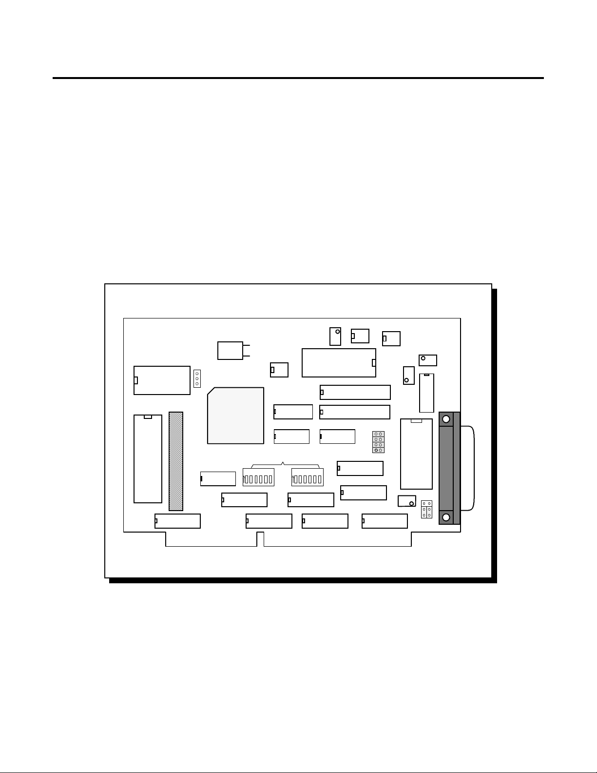
1 Introduction
The DAQ-801 and DAQ-802 are cost effective high speed data acquisition boards that plug
DAQ-800 Users Manual 8
into ISA expansi on slots in IBMTM compatible personal computers. The DAQ-800 series circuit
board provides 12-bit analog input, 32-bit digital input/output (I/O) and three 16-bit
programmable timer/counters. Each version of the DAQ-800 series board has it's own
selectable gain range. The DAQ-801 is software programmable for gains of 1, 10, 100 or 1000.
The DAQ-802 is software programmable for gains of 1, 2, 4 or 8.
The maximum sampling r ate of the DAQ- 801/802 is 40KHz. The anal og and d igital I/Os and
the external trigger, clock and reference si gnals are connected via a 37-pi n "D" type connector
which is compatible with the Keithley MetraByteTM DAS-1600. An auxiliary D37 connector is
employed to support an additional 24-bits of digital I/O. The component layout diagram for
the DAQ-800 series circuit board is depicted in Figure 1-1.
DAQ-800
20MHz
1234
ADC1241
FIFO
FIFO
sw2
56
D/A
D/A
PGA
J2
5
1
8
4
MUX
J3
3
1
8254
8255
J4
Axiliary I/O
1
3
FPGA3042
sw1
1234
Base I/O Address
56
Figure 1-1. Component Layout Diagram
Page 9

1.1 Analog Input Features
DAQ-800 Users Manual 9
The DAQ-801/802 uses one 12 bit analog-to-digital converter (ADC) to support 8 differential
(positive and negative connections) or 8 single ended analog input signals. Selection of either
single ended or differential analog inputs is software programmable. The DAQ-800 series
ADC can be configured to receive analog input voltages within the ranges of 0 to +5V or ±5V.
1.1.1 Gain Selection Ranges
The DAQ-801 provides gains of 1, 10, 100 and 1000 versus the DAQ-802, w hich provides gains
of 1, 2, 4 and 8. Tabl es 1-1 and 1- 2 show the analog input unipolar and bi polar voltage ranges
for the respective gain range.
DAQ-802 DAQ-801
GainInput RangeGainInput Range
10 to +5V10 to +5V
20 to +2.5V100 to +500mV
40 to + 1.25V1000 to +50mV
80 to +0.625V1,0000 to +5mV
Table 1-1. Unipolar Analog Input Voltage Ranges
For a gain setting of 1, the 12-bi t resolution (4096 count) provides a least signif icant bit (LSB)
value of ±1.22 mV in the 0 to +5V range.
DAQ-802 DAQ-801
GainInput RangeGainInput Range
1-5 V to +5 V1-5V to +5V
2-2.5 V to +2.5V10-500mV to +500mV
4-1.25 V to +1.25V100-50mV to +50mV
8-0.625V to +0.625V1,000-5mV to +5mV
Table 1-2. Bipolar Analog Input Voltage Ranges
For a gain setting of 1, the 12-bit resolution (±4096 count) provides a least signif icant bi t (LSB)
value of ±1.22mV in the ±5V range.
Page 10

1.1.2 Source and Trigger Mode for Analog-to-Digital Conversions
Upon initial power up, the DAQ-801/802 is in idle mode and no conversions are performed.
DAQ-800 Users Manual 10
Conversions begin upon receiving a trigger. Two types of triggers are available: internal
trigger and external trigger. The internal trigger is initiated by a software program, whereas
the external trigger is connected through hardware. The external trigger type can be either
TTL or analog. The TTL trigger input comes from pi n 25 on the main connector. The analog
trigger channel is the start channel in the scan list and it's trigger voltage is set by D/A
channel 1. When a trigger is initiated, the ADC immediately converts the analog signal into
12-bit digital data which is stored in the data FIFO (First In First Out) register. In addition to
varied triggering sources, a triggering mode is available to select whether conversions and
channel scans are completed only once or multiple times. Trigger source and trigger mode
types are software selectable.
Triggering functions are summarized as follows:
(a) Trigger sources (internal/external) :
Internal software trigger
External TTL trigger on falling or rising edge
External analog trigger with low to high or high to low transition
For the external TTL trigger, the default trigger pin on the main D37 connector is pin 25.
(b) Trigger mode:
Single -- one scan/conversion for each trigger
Continuous -- continuous scanning/conversions for one trigger
1.1.3 Scan List
The DAQ-801/802 scan list function performs high speed A/D conversions from channel to
channel enabling the user to digitize and collect data from several analog input channels
almost simultaneousl y. The scan FIF O must be programmed w ith the start and stop channel s
and also according to the scan sequence desired. When the scan list function is initiated, A/D
conversion begins from the start channel. After the conversion is completed, digitized data is
entered into the data FIFO an d the b oard sel ects the next locati on to repe at the same task. T his
process continues until the stop channel is reached. Before the scan list function is called, the
FPGA registers must be written with the start and stop channels and their corresponding
gains. If the user specifies the start and stop channels to be the same, then single channel
acquisition mode occurs. Otherwise, the scan is sequential and incremental by one. For single
trigger mod e, i t scans once and then stops. In continuous mode, scanning continues at a speed
set by the sampling rate until the desired number of scan times is reached.
Page 11

1.1.4 Sampling Rate
DAQ-800 Users Manual 11
When digitizing the analog signal, one user selectable parameter is the sampling rate which
determines how fast the analog signal is digitized. The minimum sampling rate must be at
least two times the input signal frequency to accurately recover digitized data from the
original analog input signal. The maximum sampling rate of the DAQ-801/802 is 65KHz
without auto zero ca l i bration and 3 9KHz with auto ze r o calibrati on an d i s d e r i ve d f r om the on
board 8254 chip which has three 16-bi t timer/counters. The clock input to timer1 is 2.5MHz.
Timer1 and timer2 are cascaded to generate the sampling rate pulse which in turn triggers
A/D conversion.
1.1.5 Data FIFO
DAQ-801/802 uses a data FIFO register between the output of the ADC and the ISA bus to
buffer data from the ADC output. Unlike conventional A/D boards where the di gitized data
output is fetched directly to the PC memory, the output data from the ADC is fed into the
FIFO first for temporary storage. The length of the FIFO register is 1024 sampling points and
the register circuit provides hardware flags for half full, full and empty signals. Utilizing these
signals, the b oard ca n genera te an inter rupt to the PC when the FIFO i s ha lf f ull . Once the PC
interrupt is complete, the interrupt service routine program uses the "MOVE STRING"
instruction to move the FIFO da ta directly in to PC memory at a very high speed. In this case,
it only interrupts the PC every 512 samples and thereby improves the speed of operation. In
Windows appl ications, the latency of the inte rrupt d oes not effect the i ntegr ity of the di gi tized
data as it continues into the FIFO. The status register (see Chapter 5, Table 5-1: Address map)
provides information about FIFO empty, half full and full conditions.
Page 12

1.2 Analog Output Features
In addition to the analog input channels, the DAQ-801/802 contains two analog output
DAQ-800 Users Manual 12
channels. Each channel has its own 12-bit di gital-to-analog converter (DA0 and DA1 at pins 9
and 27 on the main I /O D37 connector ). T he analog outputs a re buf fer ed and capab le of 1 mA
of output current. The output voltage range for each channel is jumper selectable as unipolar
or bipolar. The 12-bit resolution provides a LSB value of 4.88mV on the ±10V range and
2.44mV in the 0 to +10V range. Both channels use multipl yi ng D ACs which requi r e a ref erence
voltage input in addition to the 12-bit digital values. The DAQ801/802 provides an internal
reference voltage while an external reference voltage can also be supplied via jumper
configuration.
1.3 Digital I/O
The DAQ-801/802 has 32 digi tal I/O lines. Of the 32 li nes, 8 of them can be accessed through
the main D3 7 conne ctor . There are 4 inputs: I P0 throug h I P3, and 4 outputs: OP0 through OP3,
(refer to Chap ter 3, Figure 3 -3 for pin l ocations). The remain ing 24 I/O lines ar e generated by
an 8255 programmable peripheral interface chip and are accessed through the auxiliary D37
connector. The 8255 has three ports (A, B and C) and one control register. Any port can be
programmed as in put or output. Ports A and B ar e 8 bit I /O por ts whil e port C can be f urther
divided into two 4-bi t I/O ports. T he 8255 has three modes of operation whi ch are d etermi ned
by values wr itten into the control regi ster. Mode 0 i s for basic input/output config uration in
which the output port is l atched and the input por t is not. Mode 1 employs Port A or B a s the
data port while using Port C for handshake, interrupt, and digital I/O lines. Mode 2 uses Port
A as the bi-directional data port with Port B and C as control and digital I/O lines. For a
detailed functional description, the user is referred to the Intel® 8255 data manual.
1.4 Counter / Timer
The 8254 timer/counter chip on the DAQ-801/802 provides three 16-bit timer/counter
channels for time-related applications. Timer1 and timer2 are cascaded together with an input
clock of 2.5MHz and the output of timer2 is used as the sampling rate clock for the A/D
converter. T hr e e terminal s for timer 0 ar e availab l e to the user vi a the main I/O D 37 connector .
The three terminals are Pin 2 (Timer0 Out), Pin 21 (Timer0 Clk) and Pin 24 (Timer0 Gate). The
gate termina l should b e log ic high i n order for the counter to function. If gate is hel d at logi c
low, the counter is disabled.
Page 13

1.5 Interrupts
DAQ-800 Users Manual 13
The DAQ-801/802 supports AT style ISA bus interrupts which includes IRQ 2-7, 10-12 and
14-15. The selection of inter rupts is softwa re programmabl e through the reg ister setting of the
FPGA. Any interrupt conflict can be conveniently resolved by moving the selection to another
available line without opening the computer case. There are four interrupt sources from
DAQ-801/802:
End of scan
Data FIFO Half Full
Data FIFO Full
Timer0
The end of scan interrupt is normally used in conjunction with single trigger mode or in
continuous mode when the scan rate is less than 1KHz. After the scan list is completed, the
end of scan generates an interrupt to inform the computer to fetch the data.
The data FIFO half full interrupt is used during continuous trigger mode. When the FIFO is
half full, i t interrupts the PC to fetch at least 512 sample points. This interrupt works well in
the Windows environment because of interrupt latency problems inherent in the Windows
operating system.
The data FIFO full interrupt is not recommended for applications unless the interrupt routine
is executed promptly before the next data points are accepted. Otherwise an overflow can
occur and data may be lost.
Timer0 in terrupt is used in conjunction with the external ti mer at the main D37 connector. The
external cl ock pulses are connected to the time r0 clk input (pin 21) and the output of timer0
can be used as an interrupt source. When the user must interrupt the PC at a certain time
interval, timer0 can be programmed to meet the requirement.
Page 14

1.6 Software Support
Software drivers are provided to support various programming languages like Microsoft
DAQ-800 Users Manual 14
C/C++, Borla nd C/C++, Qui ckB asic, Vi sual Basi c f or MS-D OS a nd T urbo Pascal . A D ynami c
Link Library (DLL) is provided for numerous programming languages under Windows as
well as Visual Basic Controls. Software support is available on the Omega "DaqSuite" compact
disk in the following categories:
1. DAQDRIVE® Software driver
2. DaqEZ™ Data Acquisition Package
3. VISUALDAQ® Data Acquisition Package
DAQDRIVE is a low level generic driver consisting of a set of user commands that act as a
library routine for all d ata acquisition boards. Programs written for the DAQ-801/802 can be
ported to other boards in the event the user decides to change boards in the future.
DAQDRIVE is available for Window DLLs and the MS-DOS environment. In the case of
Visual Basic applications, Omega provides VISUALDAQ®. Because of it's user friendly
nature, this software is very practical for interaction with data acquisition boards and for
creating graphic presentations.
Omega also provides driver support for third party data acquisition packages such as
TestPoint® (Capital Equipment Corporation) and LabVIEW® (National Instruments). These
packages allow the user to create custom test, measurement and data acquisition applications.
1.7 Power Requirements
The DAQ-801/802 is powered directly by the +5V and +12V power source provided by the
computer bus.
1.8 Applications
The DAQ-801/802 performs the following functions: analog input (A/D), analog output
(D/A), digital I/O and timer/counter functions. Typical applications for each function are
listed as follows:
A/D conversion converts analog voltage into digital information, which enables the computer
to process or to store the signals. Typical appl ications are sensor or transd ucer measurement,
wave form acquisition/analysis and data storage. (Most sensor/transducer measurements
require signal conditioning prior to measurement by an A/D converter).
D/A conversion is the opposite of A/D conversion. This operation converts digital
information to analog voltage. Typical applications are process control and function/pulse
train genera tion. The dig ital input f unction is useful in appl ications such as contact closure or
switch status monitoring. The digital output function is useful for relay control and industrial
on/off control. A timer/counter is typi cally used for eve nt counting and pulse g eneration. It
can also be used for frequency, period or pulse measurement.
Page 15

1.9 DAQ-801/802 Specifications
Adjustable to 0
Gain Error
Adjustable to 0
Zero Error
8 Samples
Size of Scan List
without auto zeroing: 15.2µs
with auto zeroing: 25.6µs
Scan Time (channel to channel)
Twos complement
Output Data Code
-5V to +5V
Input Ranges
8 differential, 8 single ended
Channels
39 Khz (with auto-zero calibration)
65 Khz (without auto-zero calibration)
Maximum Sampling Rate
Analog Input
Analog Output
4
Input Bits
82C54
Type
3, down
Number of Counters
Timer/Counter
24 bits
I/O
(24 bits on Auxiliary Connector)
Digital I/O
DAQ-800 Users Manual 15
Gain Ranges:
Model 801
Model 802
1, 10, 100, 1000
1, 2, 4, 8
1 M ohmInput Impedance
50pAInput Bias Current
Surge Protection up to
±20 V
12-bit + signResolution
Successive ApproximationConversion type
2Channels
0 - 5V, 0 - 10V, ±5V, ±10VOutput Ranges
Straight BinaryOutput Data Coding
12-bitResolution
(8 bits on main D37 Connector)Digital I/O
4Output Bits
82C55AType
Page 16

60 mA typ, 80 mA max
-12vdc
120 mA typ, 160 mA max
+12vdc
15 mA typ, 20 mA max
-5vdc
750 mA typ, 900 mA max
+5vdc
Power Requirements
0 - 70° COperating Temperature
Environments
DAQ-800 Users Manual 16
3-7, 9-12, 14, 15Interrupt Level
0-95%Humidity
7 in x 4.8 inDimensions
Page 17

2 Hardware Configuration and Initial Setup
This section describes how to unpack and configure the DAQ-800 series circuit board.
DAQ-800 Users Manual 17
2.1 Unpacking
The DAQ-801/802 is packed in an antistatic bag to avoid possib le damage to the electrostatic
discharge se nsi ti ve components on the board . Before r emoving the product f r om i t's pr otecti ve
bag, touch both the bag and the computer chassis to establish grounding. If available, utilize a
static free work station to unpack the DAQ-801/802. Once grounding has been established,
remove the board from it's packaging and inspect it for signs of damage.
2.2 Auxiliary Connector Cable
The DAQ-801/802 auxiliary I/O connector can be accessed via a PC expansion slot by
attaching the cable assembly included with the product.
40 pin
Male
Connector
Connector
Auxiliary I/O
Main I /O
40 pin
DAQ-801/802
Female
Cable Assembly: P/N 920-0048-01A
Figure 2-1. Auxiliary Connector Cable
D37 Male
Connector
Page 18

2.3 Configuring the DAQ-801/802
DAQ-800 Users Manual 18
The user must decide the appropriate configuration for the DAQ-801/802 board d epend i ng on
the application. The D IP switch settings for SW1 and SW2 and the jumper settings f or J2, J3
and J4 must be selected before installing the board in the computer. While software
programmable configurations can be done later, the following items are jumper or switch
selectable and must be decided before installation into the PC:
1. I/O base address selection
2. D/A voltage reference, bipolar/unipolar output range.
3. Internal/external clock source for Timer 0
2.3.1 I/O Base Address Selection
Each board in the PC must have a uni que input/output a ddr ess. No tw o b oard s can shar e the
same address. Similar to a mail box, the PC processor sends data to or fetches data from this
address. Some of the I /O locations are pre-assigned standard d efault locati ons such as COM1
(3F8H) and COM2 (2F8H). Printer port locations such as LTP1 are also fixed. The I/O base
address for most other hardware is flexible and can be any value as long as that space is not
occupied. Figure 2-2 shows the location of SW1 and SW2, the base address selection switches.
DAQ-800
8254
Auxiliary I/O
8255
J4
Don't Care
1
3
20MHz
FPGA3042
SW1
1234
456
231
A A A A A
14 13 12 11 10
Base I/O Address
56
1234
2
1
A A A A A A
9 8 7 6 5 4
ADC1241
SW2
56
SW2SW1
3456
FIFO
FIFO
D/A
D/A
ON
J2
PGA
MUX
J3
Figure 2-2. I/O Base Address Selection Switches
Page 19

The I/O base address of the DAQ-801/802 is set using two DIP switches SW1 and SW2.
DAQ-800 Users Manual 19
When a switch bit is in the "ON" position, then the corresponding address line is logic 0.
When a switch bit is in the "OFF" position, then the corresponding address line is logic 1. The
I/O base address can be selected from 0000H to 7FF0H with a 0010H interval. The upper limit
of 7FF0H implies that the address has only 15 lines and the most significant bit A15 is always
0. Switches SW1 and SW2 select address lines A14 through A4. Since the board encompasses
16 register locations which require 4 address lines, (A3, A2, A1 and A0), only A14 through A4
address lines are used for base address decoding. Figure 2-3 shows several switch
configurati ons and the I/O base addresses they repr esent. The factory defa ult address setting
is 300H.
Do n't ca re
xxxxx
123456
O
N
A A A A A
14 13 12 11 10
SW1
xxxxxx
123456
O
N
SW2
A A A A A A
9 8 7 6 5 4
03 10
00000 11 1000
123456
O
N
Example1: Base I/O Address = 0310H
123456
O
N
6A D0
11010 10 1110
123456
O
N
123456
O
N
Example 2: Base I/O Address = 6AD0H
0000
Bit=0 Bit=1
xxxx Hex
0000 : 0
0001 : 1
0010 : 2
0011 : 3
0100 : 4
0101 : 5
0110 : 6
0111 : 7
1000 : 8
1001 : 9
1010 : A
1011 : B
1100 : C
1101 : D
1110 : E
1111 : F
Figure 2-3. I/O Base Address Selection
Page 20

2.3.2 D/A Voltage Reference
The digital to analog converter in the DAQ-801/802 uses a multiplying D /A converter which
DAQ-800 Users Manual 20
requires a reference voltage connection. There are two reference voltages selections available:
one is the interna l power supply +5 vdc refer ence voltage and the other is an ex ternal input.
Figure 2-4 illustrates internal/external reference voltage selection for D/A channels DA0 and
DA1. Configure jumper J3 for the desired reference as follows:
DA0 DA1
External reference Pins 2 & 3 Pins 5 & 6
Internal reference Pins 1 & 2 Pins 4 & 5
DAQ-800
20MHz
8254
Auxiliary I/O
J4
1
3
FPGA3042
ADC1241
FIFO
FIFO
PGA
8255
J2
Base I/O Address
SW1
1234
56
DA0
DA1
1234
56
SW2
D/A
D/A
J3
6
3
5
2
41
External Reference
Internal Referenc e
Figure 2-4. D/A Voltage Reference Jumper
MUX
J3
Page 21

2.3.3 Bipolar/Unipolar Output Range Selection
Each D/A output has an option of either Unipolar or Bipolar connections. In addition, the
DAQ-800 Users Manual 21
output voltage range can also be selected. Unipolar or bipolar output selection is made by
either connecting or not connecting jumper J2 as applicable for the desired output result.
Tables 2-1 and 2-2 list the combinations of jumper confi gurations for available voltage range
selections. The location and configuration options for jumper J2 are shown in Figure 2-5.
D/A0 output voltage Pins 2 & 6Pins 1 & 5
-5V to +5V, bipolarConnectConnect
-10V to +10V, bipolarOpenConnect
0 to +5V, unipolarConnectOpen
0 to +10V, unipolarOpenOpen
Table 2-1. DA0 Output Voltage Ranges
D/A1 output voltage Pins 4 & 8Pins 3 & 7
-5V to +5V, bipolarConnectConnect
-10V to +10V, bipolarOpenConnect
0 to +5V, unipolarConnectOpen
0 to +10V, unipolarOpenOpen
Table 2-2. DA1 Output Voltage Ranges
Page 22

DAQ-800
DAQ-800 Users Manual 22
8254
Auxiliary I/O
J4
1
3
20MHz
FPGA3042
ADC1241
FIFO
FIFO
PGA
D/A
D/A
J2
1
MUX
8
8255
SW1
1234
Base I/O Address
56
1234
SW2
56
J3
DA0 DA1
J2
Connect: 5v range
Open: 10v ra nge
Connect: bipolar
Open: unipolar
Connect: bipolar
Open: unipolar
Connect: 5v range
Open: 10v ra nge
5678
1234
Figure 2-5. Bipolar/Unipolar Output Range Selection Jumper
Page 23

2.3.4 Timer0 Internal/External Clock Selection
The timer0 connection is used f or timing or counting applicati ons. Jumper block J4, shown in
DAQ-800 Users Manual 23
Figure 2- 6, is used to sele ct the internal or external clock w hich connects to the clock input of
timer0 at pin 21 on the main I/O D37 conne ctor. When configured for an external input, the
timer/counter can be used for pulse counting an external event. Configure jumper J4 as
necessary for the desired clock input:
Internal 2.5MHz clock Jumper pins 1 & 2 on J4 (timer operation)
External clock Jumper pins 2 & 3 on J4 (counter operation)
DAQ-800
8254
Auxiliary I/O
8255
20MHz
J4
1
3
FPGA3042
SW1
1234
Timer 0 clock source
Base I/O Address
56
1234
J4
1
2
3
ADC1241
FIFO
FIFO
J2
SW2
56
Internal 2.5MHz
External clock
D/A
D/A
PGA
MUX
J3
Figure 2-6. Internal/External Clock Selection Jumper
Page 24

2.4 Installation under Windows95/98®
Windows95/98 maintains a registry of all known hardware installed in a computer. Inside
DAQ-800 Users Manual 24
this hardware r e gistry Windows k eeps track of all system resour ces such as I/O locations, IRQ
levels and DMA channels. The "Add New Hardware Wizard" utility in Windows95/98 was
designed to add new hardware and update this registry.
An "INF" fi le is included wi th the DAQ-801/802 to allow easy configuration in the Wind ows
environment . Windows95/98 uses the "INF" file to determine the system resources required
by the DAQ-801/802, searches for available resources to fill the boards requirements and then
updates the hardware registry with an entry that allocates these resources.
Windows will not automatically configure the DAQ-801/802. The user is required to
manually confi gure the hardware to match the resources that Windows95/98 allocate s to the
DAQ-801/802. Another option is to use the "Devi ce Manager" to change the system resources
allocated to match the configuration of the hardware.
2.4.1 Using the "Add New Hardware Wizard"
The following instructions provide step-by-step instructions for installing the DAQ-801/802
with Windows by using the "Add New Hardware Wizard". Select Start/Help from the
Windows95/98 start bar for additional information on this utility.
1. Start the Add New Hardware Wizard utility. The icon for this utility is located in
the Windows95/98 control panel.
2. A dialog box will appear which initiates the "Add New Hardware Wizard" utility.
Select the "Next" button to continue.
3. An option box appe ars al lowi ng the choi ce of havi ng Wind ows automa ticall y d etect
the new hardware. Select the "No" option. The dialog in the box recommends
selecting the "Yes" option, but unless the hardware is installed with standard I/O
and IRQ levels, this option will fail. Select the "Next" button to continue.
4. A hardwar e type l ist box shoul d appear . Select the "Other D evices" ty pe on the li st
and then select the "Next" button to continue.
5. A list box opens wi th manufacturers on the left a nd the associated boa rd models on
the right. Select the "Have Disk" button.
6. An "Install From Disk" dialog box should pop open. Insert the customer CD-ROM
with the DAQ-801/802 INF files on it, select the correct drive letter and then select
the "OK" button. Windows95/98 automatically browses the root directory for an
INF file that defines configurations for the circuit board. If no INF files are found,
click the " Browse" button and sea rch the Wi n95/98 sub d irectory on the install ation
CD for the file “DAQPCARD.inf” . (The file name is not required. After finding the
directory containing the INF files, Windows will choose the correct file).
7. Your computer should read the INF file and display a list of data acquisition board
models supported by Windows95/98. Select the DAQ-801 or DAQ-802 model name
from the list and select the "Next" button to continue.
Page 25

8. A dialog box will appear with an unused I/O range and IRQ resources that
Windows has f ound avai l ab l e i n the registry. Wi nd ow s has assi g ned these resources
DAQ-800 Users Manual 25
to the DAQ-801/DAQ-802. Review these settings carefully before proceeding.
2.4.2 Changing Resources with Device Manager
The following instructions provide step-by-step instructions on viewing and changing
resources of the DAQ-801/802 in Windows95/98 using the "Device Manager" utility. Select
Start|Help from within Windows for additional information on this utility.
Either take notes of the resources being allocated to the new hardware or have
Windows95/98 print a copy. The D AQ-801/802 must then be manually configured
to match these resources. Windows will not automatically configure the
DAQ-801/802 board.
9. Another dialog box will open when the installation is complete. Select the "Finish"
button to end the software installation.
10. Windows will then instruct the user to shut down the computer and install the
hardware. Select the "Yes" button to shut down the computer. When
Windows95/98 sends the "safe" message, power down the computer.
11. Either manually configure the DAQ-801/802 to match the resources allocated by
Windows, or use the "Device Manager" i n Windows95/98 to change the previ ously
allocated system resources to match your preferences.
1. Double click the "System" icon inside the Control Panel folder. This opens up the
System Properties box.
2. Select the "Device Manager" tab located at the top of the System Properties box.
This lists all hardware devices listed inside the Windows95/98 registry. Additional
information is available on any of these devices by clicking on the device name and
then selecting the "Properties" button.
3. Double click the devi ce group "Data_Acquisiti on". The DAQ-801/802 model name
should appear on the list of hardware.
4. Double click the DAQ-801/802 model name and a properties box should open.
Page 26

5. Click the "Resources" tab located along the top of the properties box. Confirm
Windows95/98 has allocated resources for the DAQ-801/802 that match the board's
DAQ-800 Users Manual 26
hardware confi guration. To modify any of the resource settings select the resource
name and click the "Change Setting" button. Sele ct "Cancel" to exi t without maki ng
changes.
6. When the "Change Settings" button is selected, an "Edit Resource" window will
open. Insid e thi s wi ndow, cli ck on the up/dow n arrow s to the rig ht of the resour ce
value. This scrolls through all of the allowable resources for your hardware. Note
the Conflict Inf ormation at the bottom of the window . Do not sele ct a resource that
causes a conflict with any other installed hardware. Select "OK" to save your
changes or "Cancel" to abort changes.
7. You are required to manually configure the DAQ-801/802 to match the resources
allocated by Windows95/98.
2.5 After Completing Configuration
The DAQ-801/802 is now configured and ready f or use. Depending on the type of application
software to be used, the user may want to review one or more of the following:
1. Chapter 4 of this d ocument provi des ba sic theory of operati on for user s tha t wish to
learn technical details about the operation of the DAQ-801/802.
2. For users that want to program the DAQ-801/802 with direct transfers to the
register set, Chapter 5 provides an address map and a detailed description of each
I/O register.
3. Users that wish to write custom application software without programming the
DAQ-801/802 directly should consult the DAQDRIVE software reference manual.
DAQDRIVE provides a library of data acquisition subroutines for all Omega data
acquisition cards and is included free of charge with the DAQ-801/802.
4. For third party data acquisition software such as LabTech Notebook®, LabVIEW®,
TestPoint® or SnapMaster®, consult the documentation provided by the software
manufacturer.
Page 27

3 Field Wiring
Before completing any installation or connection, ensure power is not applied to the computer
DAQ-800 Users Manual 27
or external circuits. Install the DAQ-801/802 as directed by the procedures in Chapter 2:
Hardware Configuration and Initial Setup. The main I/O D37 connector on back of the PC
contains all the analog input and output signal pins. The auxiliary connector is used for
digital I/O connection. Both connectors and Omega cables are Keithley MetroByte
DAS-1600 compatible.
3.1 I/O Terminal Connection
The user can connect either one or both I/O connectors on the DAQ-801/802 to the external
UIO-37 screw terminal block shown in Figure 3-1. The UIO-37 has 37 numbered screw
terminals that correspond one to one to the pins on both the main I/O and auxiliary D37
connectors on the DAQ-801/802. The UIO-37 provides a convenient connection for external
wiring and is avai l abl e w i th either a male or female D37 connector. Wire gage 16 through 28 is
recommended for screw terminal connections.
D37 Connector (Male or Female available)
TM
Screw Terminal Connections
Ground
Figure 3-1. UIO-37 Screw Terminal Block
Page 28

The UIO-37 is connected to the PC using the Omeg a CP-DAQ D37 f emale to mal e 3 foot cable
DAQ-800 Users Manual 28
as shown in Figure 3-2. The CP-DAQ cable male end connects to the UIO-37 female D37
connector and the female end connects to the main I/O and auxiliary connectors on the
DAQ-801/802.
Computer
Main
CP-DAQ
Auxiliary
19
18
19
18
3
2
1
3
2
1
UIO-37
19
CP-DAQ
D37 female to male
3 foot cable
1
18
19
18
3
2
3
2
1
UIO-37
Figure 3-2. Connection of UIO-37 Terminal Blocks to DAQ-800 Series Connectors
Page 29

3.2 D37 Connector Pin Diagrams
DAQ-800 Users Manual 29
Analog I/O connections are made through D37 connectors as shown in Figure 3-3.
Analog GND
-CH0
-CH1
-CH2
-CH3
-CH4
-CH5
-CH6
-CH7
DA0 Ref
DA0 Out
Vref (-5V)
Power GND
IP1
IP3
OP1
OP3
Timer0 Out/-15V
+5V
Main I/O Connector
19
18
17
16
15
14
13
12
11
10
9
8
7
6
5
4
3
2
1
37
36
35
34
33
32
31
30
29
28
27
26
25
24
23
22
21
20
+CH0
+CH1
+CH2
+CH3
+CH4
+CH5
+CH6
+CH7
Analog GND
Analog GND
DA1 Out
DA1 Ref
IP0/Ext TTL T r i g / Tim er 1 C l k
IP2/Ti mer0 Gate
OP0
OP2
Timer0 Clk/+ 15V
Timer2 Out
Auxiliary Connector
DIG COM
+5V
DIG COM
DIG COM
DIG COM
DIG COM
PB0
PB1
PB2
PB3
PB4
PB5
PB6
PB7
19
18
17
16
15
14
13
12
11
10
9
8
7
6
5
4
3
2
1
37
36
35
34
33
32
31
30
29
28
27
26
25
24
23
22
21
20
OP=Digital Output (4 bit port) PA=Port A (bit 0-7)
DA=Digital to Analog Channe l
IP=Digital Input
PC=Port C (bit 0-7)
PB=Port B (bit 0-7)
PA0
PA1
PA2
PA3
PA4
PA5
PA6
PA7
PC0
PC1
PC2
PC3
PC4
PC5
PC6
PC7
DIG COM
+5V
Figure 3-3. D37 Pin Diagrams
Pins 11 through 18 and pins 30 through 37 are the available analog input channels. For
differential input, the eight available channels are numbered 0 through 7 and each channel
consists of one positive input (+CHx) and one negative input (-CHx). For single-ended
operation, the available channels are numbered 0 through 7 with the - CHx i nputs connected to
ground.
Page 30

3.3 Analog Input Field Wiring
(
)
Q
DAQ-800 Users Manual 30
3.3.1 Single Ended Input
The analog input signals can have either single ended or differential inputs. Figure 3-4
illustrates field wiring for single ended inputs. There are 8 single ended channels available,
each with a positive (+CHx) and negative (-CHx) connection. Connect the (+) wire to the
desired input channel terminal and the (-) wire to the UIO-37 analog ground at terminals 19
and 29.
If a high electrical noise environment exists, individual shielded wiring is recommended.
Keep the signal lines as far from the power line as possib l e and never bund l e si gnal cabl es and
high current or voltage cables in the same harness. High electric field intensity may
deteriorate or interfere with the signal being measured.
Vin0
+
Vin1
+
.
.
Vin7
.
+
External Trigger
+CH0
-CH0
+CH1
-CH1
+CH7
-CH7
IPO/EXT
GROUND
37
18
CP-DA
36
17
30
11
25
19
29
DAQ-801/802
ADC1241
FIFO
PGA
FIFO
145
J2
8
Gain,UI/BI
MUX
Base I/O Ad dre ss
D/A
sw1
sw2
D/A
J3
3
14
Referenc e
UIO-37
Terminal Block
Figure 3-4. Single-Ended Analog Input Field Wiring
FPGA3042
20MHz
DAQ-800
J4
1
8254
3
8255
Interrupt
Mode
123456123456
Axiliary I/O
Page 31

3.3.2 Differential Input
Differential input signals normally have three wire connections: (+) signal input, (-) signal
(
)
gg
Q
DAQ-800 Users Manual 31
input and a ground connection. Figure 3-5 illustrates differential input field wiring. Connect
the (+) input to +CHx and the (-) input to the corresponding -CHx terminal on the UIO-37.
The ground wires can be tied together and connected to the UIO-37 analog ground at
terminals 19 and 29. T he advantage of differential input wiring is that noise picked up along
the input signal lines will be canceled out at the instrumentation amplifier on the
DAQ-801/802 and only the pure signal will remain at the input to the A/D converter. For
noise levels greater than 1 or 2 LSB, differential configuration will definitely improve the
accuracy of the input signal.
Sensors with only two input wires, (no ground wire), can still be connected for differential
operation. Connect the signal input wires as described above and omit the ground
connection.
DAQ-801/802
PGA
145
J2
8
Gain,UI/BI
MUX
D/A
D/A
J3
3
14
Referenc e
UIO-37
Terminal Block
Ground
Vin0
Vin1
Vin7
+
+
+
-
+CH0
-CH0
+CH1
+CH7
External Tri
-CH1
-CH7
37
18
36
CP-DA
17
30
11
25
er
19
Ground
29
Figure 3-5. Differential Analog Input Field Wiring
20MHz
Base I/O Ad dre ss
sw1
sw2
FPGA3042
DAQ-800
J4
1
8254
3
8255
Interrupt
Mode
123456123456
Axiliary I/O
ADC1241
FIFO
FIFO
Page 32

3.4 Analog Output Field Wiring
DAQ-800 Users Manual 32
Typical analog output field wiring is shown in Figure 3-6. In this case, two shielded conductor
cables are recommended. The positive output is connected to the UIO-37 terminal block at
terminal 9 for DA0 and terminal 27 for DA1. The negative output is connected to analog
ground at terminals 19 and 29. The D/A output requires either an internal or external
reference. For the internal reference configuration, no connection is required at terminals 10
and 26 for DA0/DA1 reference i nputs. If the external reference confi guration is used, then an
external reference voltage must be applied to the UIO-37 terminal block at terminal 10 for
DA0 and terminal 26 for DA1. The external reference voltage can be either fixed or a varying
timing signal. Since the DAQ-801/802 uses a multiplyi ng D/A converter the output voltage is
the result of multiplying the D/A output by the reference voltage input. If the reference
voltage is fixed (non time varying), then the reference voltage only affects the magnitude of
the output voltage. If the reference signal is time varying, then the D/A output signal can
become an amplitude modulated signal.
DAQ-801/802
LOAD 0
LOAD 1
DA0
9
10
Vref DA0
CP-DAQ
DA1
27
UIO-37
Terminal Block
Vref DA1
Ground
26
19
29
()
Figure 3-6. Analog Output Field Wiring
20MHz
Base I/O Ad dre ss
sw2
DAQ-800
J4
1
8254
3
FPGA3042
8255
Interrupt
Mode
123456123456
sw1
Axiliary I/O
ADC1241
FIFO
PGA
FIFO
145
J2
8
Gain,UI/BI
MUX
D/A
D/A
J3
3
14
Referenc e
Page 33

3.5 Timer/Counter Field Wiring
The DAQ-801/802 has three 16-bit timer/counters. Timer1 and timer2 are used to generate the
DAQ-800 Users Manual 33
pacer clock for the A/D function. Timer0 is availa ble for the user and becomes a timer if the
input clock is connected to the i nternal 2. 5MHz clock. ( For config uration informati on refer to
Chapter 2, section 2.3.4: Internal/External Clock Selection). The output of thi s timer is pi n 2 on
the main I/O connector, (UIO-37 terminal 2). The frequency of this output signal will depend
on how the counter is programmed. A gate signal at pin 24 (main I/O D37) controls the
output signal. When the gate is opened , the output at pin 2 b ecomes active. When the gate is
closed or connected to ground, the output becomes 0.
When the DAQ-801/802 is configured for external clock, then the timer0 output changes to a
16-bit counter function. The counter can be used to count pul ses a nd the results can b e read by
the software. The signal to be counted i s connected at pin 21 and the counter can b e enab l ed or
disabled by controlling the gate signal at pin 24. If the switch is open, the counter is enabled
and any pulses present at pin 21 will be counted. If the switch is closed, the counter is
disabled. When the counter overflows, a pulse will be generated at terminal 2 at the output
clock. Figure 3-7 illustrates timer0 field wiring.
DAQ-801/802
20MHz
Base I/O Ad dre ss
sw1
sw2
FPGA3042
DAQ-800
J4
1
8254
3
8255
Interrupt
Mode
123456123456
Axiliary I/O
Signal
Source
Switch
External
Gating
Timer 0 CLK
GND
Gate
21
7
24
CP-DAQ
ADC1241
FIFO
PGA
FIFO
145
J2
8
Gain,UI/BI
MUX
D/A
D/A
J3
3
14
Referenc e
UIO-37
Terminal Block
2
Timer0 output
Figure 3-7. Timer/Counter Field Wiring
Page 34

4 Theory of Operation
4.1 Signal Flow
DAQ-800 Users Manual 34
The DAQ-801/802 signal flow block diagram is shown in Figure 4-1. The heart of the circuit is
the Field Programmable Gate Array (FPGA). This FPGA controls the timing required for A/D
conversion, D/A output and d igital I/O. There is a common b us on the board which car ries
the binary data g enerated by A/D conversion and binar y data sent to the D/A converter. The
data coming in fr om the digital input port or going out to the digi tal output port also passes
through the common bus. The common bus is separated from the ISA bus by a 16-bit data bus
buffer.
Ref
8 CHs
8-CH
MUX
Main D-37 Connector
PGA
Channel
Comp
Gain
FPGA
Scan List
(channel+gain)
12-bit A/D with
Auto-Zeroing &
Self Calibrating
Trigger Source
and MODE
12bit DA1
Auxiliary D-37
Ref
8-bit
8-bit
4-bit
4-bit
12bit DA0
8255A
PA
PB
PC1
PC2
U/B
1,2
Gain
Polar
IRQ 3-7,9-12,14,15
4-bit
Input
4-bit
Output
Interrupt
I/O Base
Select
Control
Select
Status Register
Interna l Bu s
div 4
buffer
Buffers
12-bi t + sign
1K X 16
FIFO
8254
Timer0
Timer1
Timer2
10MHz
ISA BUS
Figure 4-1. DAQ-801/802 Signal Flow Block Diagram
The FPGA sends out the necessary information to select the multiplexer, the gain of each
channel and sampling rate. The CPU sends the appropriate data to the registers residing
inside FPGA. When these settings are complete, the input signal comes through the analog
multiplexer and to the A/D converter via the Programmable Gain Amplifi er (PGA). The A/D
converter initiates conversion upon commands from the FPGA.
Page 35

The output of the A/D converter is 12-bit binary data and is in 2s complement format. The
stream of A/D output is fed into a 1K X 16 FIFO (First in Fir st Out) and the CPU then reads
DAQ-800 Users Manual 35
the data. The CPU can rea d data afte r each A/D conversion, a fter the FIF O is hal f full and all
at once using the "MOVE STRING" operation. Since the end of A/D conversion, FIFO half full
and FIFO full can generate interrupts to the processor, efficient data acquisition can be
achieved without using polling techniques. The FIFO is located at Base +0 address and any
read from this location will yield 16-bit data to the CPU. This 16-bit data, which is right
justified, will have the upper four bits either 0 or 1 depending on whether it is positive or
negative. The data FIFO should always be emptied prior to data acquisition. When the FIFO
is emptied by the host, the empty flag is set to "1". If there are one or more samples left in the
data FIFO, the empty flag is set to "0".
Commencement of A /D conve r si on is initiate d by a tri g g er from the FPGA. The tr i g g er sour ce
can be a software trigger or an external trigger. The software trigger is generated by writing
an output command to I nd e x register 2 , (refer to Chapter 5: A d d r e ss Map) . Each time a trigger
occurs, conversion is initiated and data is acquired. One trigger that stimulates one A/D
conversion is referred to as single trigger mode. In continuous mode, the system continuously
performs A/D conversions at a specified rate once it is triggered. This rate is referred to as
sampling rate. The sampling rate is derived by cascading timer1 and timer2 together with a
2.5MHz clock connected to the input of timer1. The sampling rate is a maximum of 40 kHz.
If the analog si gnal is coming from a singl e channel, then the ana log multiplex er is fixe d. All
converted digitized data will belong to a single analog signal. To observe several channels
almost simultaneously, the scan operation must be performed. Scan operation requires
specifying the start and the end channels. This is completed by writing a byte consisting of
start and end channels to the FPGA register. When the scan sequence convenes, the trigger
signal starts the A/D sampl ing and simul taneously send s a signal to switch the mul tipl exer to
the next channel. The trigger signal starts A/D sampling and then signals the scan FIFO to
switch the multiplexer to the next channel. While waiting for A/D conversion to finish, the
next selected analog signal is settling down at the instrumentation amplifier. When the End Of
Conversion pulse (EOC) appears indicating A/D conversion is completed, the converted data
is written into the data F IFO. T he same proce ss r epeats until the end of the channel scan l ist i s
reached. In single trigger mode, the FPGA will scan once and stop. In continuous mode, the
FPGA scans fr om the start channel to the end cha nnel and then waits for the next sampling
clock. Sampl ed data is se que ntially stor ed in the data F I FO a nd read b y the pr oce ssor . Data for
each channel must be sorted out in continuous mode operation.
D/A operation is performed by sending 12-bit data through the data buffer to the selected
D/A channel. The strobe signal necessary for latching the 12-bit data to the register inside
D/A converter is ge nerate d by FPGA. The d ata sent to Base +8 goes to channel 0 and the da ta
sent to Base +A goes to channel 1.
4.2 Analog Input
The DAQ-801/802 provides 8 differential analog input channels. Single ended analog input
channels can be configured by wiring the (-) Chx input to analog ground. Selecting one of the
Page 36

8 channels for A/D conversion utilizes the DAQ-801/802 input multiplexer. The multiplexer
has input over-voltage protection circuit which protects the analog input circuit when
DAQ-800 Users Manual 36
transient voltage occurs. The output of the multiplexer is connected to the PGA which is
configurable for gains of 1, 10, 100 or 1000 for the DAQ-801 and gains of 1, 2, 4 or 8 for the
DAQ-802. The maximum voltage output of the PGA is limi ted to ±5V. The maximum analog
input range at the multi plex er i s al so ±5V, the refor e various g ains can b e selecte d to optimi ze
the accuracy of the input signal for data conversion. For instance, if the input signal falls
within ±40 mV, the DAQ-801 can be set for a gain of 100 which will yield a voltage ±4V at the
output of PGA. If the input signal is only ± 0.625V, then the DAQ-802 with a gain of 8 can be
chosen to get the maximum accuracy. The output of the PGA is then connected to the
sampling A/D converter.
The sampling A/D converter has a 12-bit 2s compleme nt binary output. The converter type is
successive approximation and its conversion time is 15. 2µs w i th non auto zero and 25.6µs wi th
the auto zero function. Thus, selecting the auto zero function will slow data acquisition. The
A/D converter can be calibrated across it's full range. This calibration is completed during the
initial system set up and is not required again once set up is finished.
4.3 Analog Output
The 12-bit data sent to Base +8 location by the processor will travel from the ISA bus to the
internal b us an d get to the latch at the D /A conve rte r of channel 0. Whe n the latch recei ves the
new data, it goes thr ough digital to analog conver sion and the analog voltage correspond ing
to the binary value appears. Each binary value will get a corresponding analog voltage. The
analog output voltage is then buf fered through operation amplifie r to pin 9 of the main I/O
connector. The buffered amplifier is used to increase the output driving capability. Any 12-bit
data sent by processor to address Base +A will terminate at the latch of D/A channel 1. The
same type of buffered circuit is attached to the output of channel 1 D/A converter.
The D/A converter is a multiplying D/A converter which requires a reference voltage. This
reference vol tage is provided by a ±5V anal og output with the buffer stage confi gured for a
gain of 1. When the buffer stage is set to a gain of 2, the output will have a maximum of ±10V.
Jumper configuration can enable the user to select a unipolar output. The reference voltage
can also be injected from an external circuit via jumper selection and does not have to be a
constant voltage. If a time var ying signal is used, then multiplyi ng this voltage with the D/A
output will result in a complex signal. Not only does the analog value sent by processor
change but the maximum magnitude also changes. If the reference voltage is not a time
varying signal, then adjusting the reference voltage will only change the D/A output range.
The D/A output voltage can thus be customized by feeding in the appropriate reference
voltage.
Page 37

4.4 Digital I/O
DAQ-800 Users Manual 37
The digital I/O function of the DAQ-801/802 provides a 4-bit TTL compatible input and
output. Both are accessed through the main I /O connector. Digital data fl ow is controlled by
the FPGA. In addition to the 4 bit digital I/O, there is a 82C55 programmable peripheral
interface chip on the board which supplements 24 additional digital I/O lines. The 82C55 is
located at Base +C and occupies four consecutive I/O addresses. The 24 bit digital I/O is
divided into three 8-bit ports and each port can be configured for either input or output.
There are three modes of operation for 82C55: mode 0 for basic input/output, mode 1 for
digital I/O with handshake lines and mode 2 for bi-directional data transfer. The mode is
determined by the control word of the 82C55 located at Base +F. All three ports are accessed
through the auxiliary D37 connector. At power up these three ports are configured as input
ports but their configuration can be altered by writing a value to the control word register. For
detailed discussion of the 82C55 interface chip, consult the applicable Intel® data manual.
4.5 Timer/Counter
The 82C54 interface chip has three timer/counters. Timer1 and timer2 are cascaded to
generate the sampl ing clock. Only timer 0 i s available for the user. The timer/counter has a
clock input, gate control input and pulse output. When the gate control signal is low, the
timer/counter is disabled. (See Chapter 6 for detailed explanation of the 8254 timer/counter).
Page 38

5 Address Map
The address map of the DAQ-801/802 occupies 16 I/O locations. It starts from Base +0 and
Read/Write Disable/Enable DAQ-801/802
Base + 8000
82C55 8-bit Read/Write
Base + C..F
16-bit Write only D/A channel 1
Base + A..B
16-bit Write only D/A channel 0
Base + 8..9
8-bit Read/Write Scan channel register
Base + 7
8-bit Read/Write 4-bit digital I/O
Base + 6
8-bit Read only Interrupt status register
Base + 5
8-bit Read/Write Status register
Base + 4
8-bit Read/Write
Base + 3
Read 8-bit Index Register
Base + 2
Read 16-bit Data FIFO
Base + 0, 1
DAQ-800 Users Manual 38
ends with Base +F. The actual addressable registers in DAQ-801/802 are more than 16
locations. This is done by using an index register at Base +2. The contents of the index register
will address to different sets of locations when writing to or reading from Base +3. The
following table lists the address map for the DAQ-801/802.
Write 8-bit Scan FIFO
Base +0: Gain for channels 0 - 3
Base +1: Gain for channels 4 - 7
Write 8-bit Index Register
Index 0 Configuration register
1 Interru p t level s election register
2 Auxiliary control register
3 Interrupt enable register
4-7 82C54 timer/counter
Table 5-1. DAQ-800 Series Address Map
Page 39

5.1 Base + 0 / 1, Data FIFO
11
8
1,000
10
4
1000121000
1
1
DAQ-800 Users Manual 39
Read: 16-bit data will be read from the DATA FIFO into the PC. This is a 16-bit
data transfer in 2s complement format.
For positive numbers, the data format is: 0000XXXX XXXXXXXX.
For negative numbers, the data format is: 1111XXXX XXXXXXXX.
Write: Writing to Base +0 will select the gain settings for channels 0 - 3. Writing
to Base +1 will select the gain settings for channels 4 - 7. (See Table 5-2).
Gain value (GN)DAQ-802DAQ-801
Table 5-2. Data FIFO Gain Values
Each channel has 4 different gain selections and therefore two bits are required for each
channel.
Base +0 D7 D6 D5 D4 D3 D2 D1 D0
GN3 GN3 GN
2 GN2
GN
1 GN1 GN0 GN0
Gain selection for CH0 = D1/D0, CH1 = D3/D2, CH2 = D5/D4 and CH3 = D7/D6.
Base +1 D7 D6 D5 D4 D3 D2 D1 D0
GN7 GN7 GN
6 GN6
GN
5 GN5 GN4 GN4
Gain selection for CH4 = D1/D0, CH5 = D3/D2, CH6 = D5/D4 and CH7 = D7/D6.
5.2 Base + 2, Index Register
Write: 00000XXX. Writing a byte to this location sets an index in the index
register. The last 3 bits represent the index number ranging from 0 through 7.
Read: 11111XXX. The last 3 bits is the index number written. Indexing
operation occupies two I/O locations, first writing an index to the index register at address
Base +2. If the index is 0, the next byte written to Base +3 goes to the index 0 register.
Page 40

5.3 Base + 3, Index Registers
DAQ-800 Users Manual 40
After writing to the index register at Base +2, the next write to Base +3 is directed to different
index registers.
Index 0 : Configuration register, X X X X D3 D2 D1 D0, WRITE/READ:
X: not used
D3: 1 -- digital trigger digital signal can come from IP0/external
clock or from IP1/GS0/Trig
(see Base +6, bit D5)
0 -- analog trigger *see example at the end of this chapter
D2: 1 -- single trigger mode / 0 -- continuous mode
D1: 1 -- internal trigger / 0 -- external trigger
D0: 1 -- rising edge trigger / 0 -- trailing edge trigger
Index 1: Interrupt level selection register, D7 D6 D5 D4 X X X X, WRITE/READ:
D7 D6 D5 D4 IRQ Level
0000 disabled
0001 disabled
0010 disabled
0011 IRQ3
0100 IRQ4
0101 IRQ5
0110 IRQ6
0111 IRQ7
1000 disabled
1001 IRQ9
1010 IRQ10
1011 IRQ11
1100 IRQ12
1101 disabled
1110 IRQ14
1111 IRQ15
X not used
Page 41

Index 2: Auxiliary control register, D7 D6 D5 D4 D3 D2 D1 D0, WRITE ONLY:
D7: 1 -- software trigger / 0 -- no software trigger
DAQ-800 Users Manual 41
Index 3: Interrupt enable register, D7 D6 D5 D4 D3 D2 D1 D0, WRITE/READ:
D6: reserved
D5: 1 -- flush data FIFO - reset FIFO pointer / 0 -- no action
D4: 1 -- Full scale calibration uses the status bit at Base +4 to indicate
calibration. When the bit is set, calibration is completed in 5.58ms.
0 -- no action
D3: Setting thi s bit to "1" stops the scan operation i n continuous trig ger
mode. The scan function does not stop immediate l y upon se tti ng the bit to
1, it continues A /D conversion until the scan sequence is completed . A f ter
ceasing operation, continuous mode is remains set waiting for a trigger.
D2: not used
D1: not used
D0: not used
D7: 1 -- global enable (must be 1 for any interrupt) / 0 -- disable
D6: not used
D5: not used
D4: 1 -- timer0 interrupt enable / 0 -- disable
D3: 1 -- external trigger interrupt enable / 0 -- disable
D2: 1 -- FIFO full interrupt enable / 0 -- disable
D1: 1 -- FIFO half full interrupt enable / 0 -- disable
D0: 1 -- end of scan interrupt enable / 0 -- disable
Index 4.7: Read/Write 8254 timer/counter
Index 4: Read/Write timer0/counter0
Index 5: Read/Write timer1/counter1
Index 6: Read/Write timer2/counter2
Index 7: Write control word register of 8254
Page 42

5.4 Base + 4, Status Register
DAQ-800 Users Manual 42
Read: D7 D6 D5 D4 D3 D2 D1 D0
D7: 1 -- end of conversion / 0 -- EOC not finished
D6: 0 -- always 0 bipolar mode
D5: 1 -- auto zero (AZ) / 0 -- no AZ
D4: 1 -- FIFO empty / 0 -- FIFO not empty
D3: 1 -- FIFO half full / 0 -- FIFO not half full
D2: 1 -- FIFO full / 0 -- FIFO not full
D1: 1 -- BUSY. This bit is set to 1 during full scale calibration or
when the scan sequence is not yet completed.
0 -- not busy
D0: 1 -- A/D enable / 0 -- disable
Write: X X D5 X X X X D0
X: not used
D5: 1 -- AZ. Perform auto zero for each A/D conversion. Time
required: 25.6µs (slows the sampling rate if each point uses AZ
calibration).
0 -- no AZ
D0: 1 -- arming A/D conversion, awaiting trigger to start
0 -- disarm
Page 43

5.5 Base + 5 , Interrupt Status Register
D7 D6 D5 D4 D3 D2 D1 D0, READ ONLY:
DAQ-800 Users Manual 43
Read: Interrupt status bit : 1 = interrupt occurred, 0 = no interrupt
D7: not used
D6: not used
D5: not used
D4: timer0/counter0 interrupt status
D3: external trigger interrupt status
D2: FIFO full interrupt status
D1: FIFO half full interrupt status
D0: End of scan interrupt status
5.6 Base + 6, 4-Bit Digital I/O
X X X X D3 D2 D1 D0, READ/WRITE:
Read: D3 D2 D1 D0: Read the input port located on the main I/O D37
connector at pins 5, 24, 6 and 25
Write: D3 D2 D1 D0: Write to the 4-bit output port located on the main
I/O D37 connector at pins 3, 22, 4 and 23
5.7 Base + 7, Scan Channel Register
X D6 D5 D4 X D2 D1 D0, READ/WRITE:
This register is used to store channel scan information.
X: not used
D6 D5 D4: specified scan beginning channel
D2 D1 D0: specified scan ending channel
Page 44

5.8 Remaining Base Addresses
5.8.1 Base + 8 / 9, DA0
DAQ-800 Users Manual 44
D/A channel 0 output port (16-bit), WRITE ONLY, D15 D14 ------- D1 D0
5.8.2 Base +A / B, DA1
D/A channel 1 output port (16-bit), WRITE ONLY, D15 D14 ------- D1 D0
5.8.3 Base + C..F, 82C55 Programmable Peripheral Interface chip
Base +C: PIO Port A
Base +D: PIO Port B
Base +E: PIO Port C
Base +F: PIO Control word
5.8.4 Base + 8000, Board Enable/Disable
Read: Disable/Any read to Base +8000 will cause the DAQ-801/802 to be disabled.
Write: Enable/ Any write to Base +8000 will cause the DAQ-801/802 to be enabled.
5.9 Analog Trigger Example
If the user prefers to write code for the data acquisition system instead of using the
DAQDRIVE software driver, the example below demonstrates the procedures required to
perform analog trigger data acquisition:
a) Set the analog threshold voltage (or triggered voltage) by sending it's value to DA1 at
analog output channel 1 located at Base +A.
b) Program the index 0 register :
D3: 0 analog trigger
D2: single/continuous
D1: 0 external trigger
D0: rising/trailing edge trigger
c) Flush the data and scan FIFO (Index register 2).
d) Program the scan sequence start and stop channel at Base +7 and the gain for each
channel at Base +0, 1.
e) Program the 82C54 for the sampling rate at Index register 4.7
f) Arm the circuit by writing D0=1 to Base +4.
Page 45

6 8254 Timer/Counter
Read/Write the least significant byte first
1
1
Read/Write most significant byte only
0
1
Read/Write least significant byte only
1
0
Counter latch command
0
0
Action
RW2
RW1
DAQ-800 Users Manual 45
6.1 Introduction
The timer/counter uses the industrial standard 8254 which provides three independent 16- bit
counters, each capable of handling clock inputs up to 10Mhz. Two of the timer/counters are
cascaded toge ther to provide the sampli ng clock for A nalog to Digital converter. Onl y timer0
is availa ble to the user. When the intern al 2.5MHz clock is used as the input to timer0, thi s
timer/counter becomes a timer . The output can be used for ti ming applications such as real
time clock, digital one - shot, pr og r ammable rate g ene ra tor or squar e w ave g ene ra tor . W hen the
clock input to timer0 is ex ternal, it operates as a counter . Eithe r timer or counte r operation i s
jumper selectable, (see Chapter 2, section 2.3.4) . The timer0/counter 0 output and the exter nal
pulse input (Timer0 Clk) can be accessed at the main D-37 connector.
6.2 Functional Description
The 8254 timer/counter occupies four consecutive I/O locations:
location 1 - timer0/counter0
location 2 - timer1/counter1
location 3 - timer2/counter2
location 4 - control word
The control word is used to conf igure dif ferent operations of timer/counter. When the board
is initially powered up, the state of the 8254 is undefined. It is programmed by writing a
control word to the fourth location and then an initi al count to the first location. The contr ol
word for timer/counter 0 is as follows:
D7 D6 D5 D4 D3 D2 D1 D0
0 0 RW1 RW0 M2 M1 M0 BCD
1. RW is defined as Read/Write, (see Table 6-1):
then the most significant byte
Table 6-1. Control Word Read/Write Actions
Page 46

2. M is defined as Mode of operation, (see Table 6-2):
mode 5 : Hardware triggered strobe
101
mode 4 : Software triggered strobe
001
mode 3 : Squarewave mode
110
mode 2 : Rate generator
010
mode 1 : Timing retriggerable one-shot
100
Mode 0 : Event Counting
000
ModeM0M1M2
DAQ-800 Users Manual 46
Table 6-2. Control Word Modes of Operation
3. BCD entries are as follows: 0 = Binary count / 1 = BCD count
6.2.1 Write Operation
The 8254 16-bit counters are down counters. When programming, the initial count format is
specified in the control word and therefore the control word must be written before the initial
count.. For instance, if RW1 RW0 is written as 11, then the initial count format is to write the
least significant byte (LSB) first and then the most significant byte (MSB). After writing the
initial count to timer/counte r0, the first pulse appeari ng at the cl ock input (Timer 0 Clk at pi n
21 of the main I/O D37 connector: Figure 1.2) will load the value to the counter and the
second pulse will initiate the countdown.
6.2.2 Read Operation
The value of the timer/counter0 can be read without disturbing the count in progress. The
read format depends on how RW1 RW0 is written i n the control word register. If RW1 RW0 is
written as 01, then every time the counter is read, only the LSB is received. If RW1 RW0 is
written as 11, then the fi rst read is the LSB and the second read is the MSB. The control word
needs to be wri tten only once unl ess it's used for latchi ng oper ation. T he 16-b it counter can b e
read any time in LSB-MSB sequence. It is possible during LSB-MSB read operation, when the
LSB is read, that a carry bit can be generated by the LSB counter which increments the MSB by
one. As the MSB i s read, the 16-bi t number results are then erroneous. In order to avoid thi s
ambiguous resul t, the gate i nput (T imer0 Gate at pin 24 on the main I /O D37 connector) must
be disabled to stop counting or the latch command must be used. The latch command will
instantly tr ansfer the 16-bit val ue from the output of the counter to a latch. Once the data is
latched, then read the counter.
For example, a control word with the following data is written into the control word register:
D7 D6 D5 D4 D3 D2 D1 D0
0 0 1 1 0 0 0 0 30H Timer/Counter 0
Page 47

This control word (3 0H) completes Read/Write w i th the L SB first a nd the n the MSB in mode 0
for counting events employing binary count format. After the control word is written, then
DAQ-800 Users Manual 47
write an initial count with the LSB first and the MSB next. Assuming the Timer0 Gate is
enabled, the counter will start to count down with each pulse. To read the 16-bit count at
anytime, the following latch command can be issued to the control word register:
D7 D6 D5 D4 D3 D2 D1 D0
0 0 0 0 X X X X 0H X = not used
This command will latch the 16-bit count from the output of the timer/counter 0 to a latch.
Two subsequent read operations must be completed before the next latch command can be
issued. If the data is not read, a following latch command will not update the new count.
6.3 Mode Definition
6.3.1 Mode 0 (Event Counting)
This mode i s used for event counti ng. The timer/counte r0 output (Time r0 Out at pin 2 on the
main I/O D37 connector ) can be used for a n inter rupt sig nal at the ter minal count. T he output
is low when the control word is written and will remain low until the counter reaches zero.
The timer/counter0 output then goes high and will remain high until a new count or a mode 0
control word is written. The initial count is loaded to the counter on the next clock pulse and
therefore the first clock pulse does not decrement the counter. Timer/counter0 output will go
high at N+1 clock pulses after the initial count is written. The Timer0 Gate can control
counting after the counter is programmed. When the Timer0 Gate = 1, the counter will count.
When the Timer0 Gate = 0, the counter will not count.
6.3.2 Mode 1 ( Timing Applications)
This mode is defined as hardware retriggerable one-shot and is used for timing applications.
The inte rnal 2.5Mhz clock can b e sel ected and the one-shot time d urati on can b e prog rammed
by the initial count. Timer/counter0 output is high and goes low following a trigger at the
Timer0 Gate. The output will remain low until the counter reaches zero and then goes high
until it is triggered again. (Detailed explanation of Mode 0 through Mode 5 can be found in
the applicable Intel ® 8254 data manual).
6.4 Accessing the Timer/Counter
There are two locations to be accessed for timer/counter0: one is the control word location
(same location for latch command) and the other is the Read/Write location. These two
locations are accessed by indexed addressing. Indexed addressing requires selecting the
content of the index register first, before reaching the actual location. Therefore two
instructions must b e executed for each access. The fi rst instruction chooses the index number
at Base+2 for direction and the next instruction accesses the actual location at Base+3.
"Index_reg" represents Base address + 2 and "port" represents Base address+3.
Page 48

To write a control word or latch command to the control word location:
a) outp(index_reg, 7) - selecting index register 7
DAQ-800 Users Manual 48
Writing an initial count to counter 0:
Reading the current count at timer/counter 0:
b) outp(port, value) - sending control word or latching command,
value is a control word or 0H for latching
a) outp(index_reg,4) - selecting index register 4 where Timer/counter 0 is located
b) outp(port,value0) - sending the initial count of LSB
c) outp(port,value1) - sending the initial count of MSB
a) outp(index_reg,4) - selecting index register 4 where counter 0 is located
b) value0=inp(port) - reading the LSB
c) value1=inp(port) - reading the MSB
Page 49

6.5 Programming Examples
DAQ-800 Users Manual 49
Listing 1. 8254 Programming Example 1
#include <conio.h>
#include <stdio.h>
//=======================================
// base_address+2: index register
// base_address+3: data port address
//
//
// index register register in 8254
// index4: timer/counter 0
// index5: timer/counter 1
// index6: timer/counter 2
// index7: control register
//
// To access one of the register in 8254 need two steps:
// step 1: write the index number of 8254 register to IO address base+2
// step 2: read/write base+3 to access the selected register in 8254
// Example: write 30H to control register of 8254
// step 1: outp(0x302, 7); assume base address is 300h
// index register is 300h+2=302h
// step 2: outp(0x303,0x30) data port address is 300h+3=303h
// write 74H to control register in 8254
//=======================================
void main(){
unsigned base_address = 0x300;
unsigned short byte_LSB;
unsigned short byte_MSB;
outp(base_address+0x8000, 0); // Enable the DAQ-801/802 board
//=======================================
// This example programs counter 0 of 8254 in mode 0 with initial value
// of 2675H, then reads the value of counter0 using simple read operation
// and display the higher byte and lower byte on the screen.
//=======================================
outp(base_address+2, 7); //The 8254 control register address
outp(base_address+3, 0x30); // Set control register
outp(base_address+2, 4); // Select timer index
outp(base_address+3, 0x75); // Low byte
outp(base_address+3, 0x26); // High byte
printf("Press any key to read the counter value, press ESC to quit\n");
do {
byte_LSB = inp(base_address+3); //Read the least significant byte
byte_MSB = inp(base_address+3); //Read the most significant byte
printf("High byte: %3d, Low byte: %3d\n",byte_MSB, byte_LSB);
}
while (getch() != 0x1b);
}
Page 50

Listing 2. 8254 Programming Example 2
DAQ-800 Users Manual 50
#include <conio.h>
#include <stdio.h>
void main(){
unsigned base_address = 0x300;
unsigned short byte_LSB;
unsigned short byte_MSB;
outp(base_address+0x8000, 0); // Enable the DAQ-801/802 board
/**************************************************************/
/* This example programs counter 0 of 8254 in mode 0 with initial value */
/* of 2675H, then reads the value of counter0 using Counter Latch Command */
/* and display the higher byte and lower byte on the screen. */
/**************************************************************/
outp(base_address+2, 7); //The 8254 control register address
outp(base_address+3, 0x30); // Set control register
outp(base_address+2, 4); // Select timer index
outp(base_address+3, 0x75); // Low byte
outp(base_address+3, 0x26); // High byte
printf("Press any key to read the counter value, press ESC to quit\n");
do {
outp(base_address+2, 7); //Select control register of 8254
outp(base_address+3, 0); //Counter Latch Command
outp(base_address+2, 4); //Select counter 0 of 8254
byte_LSB = inp(base_address+3); //Read the least significant byte
byte_MSB = inp(base_address+3); //Read the most significant byte
printf("High byte: %3d, Low byte: %3d\n",byte_MSB, byte_LSB);
}
while (getch() != 0x1b);
}
Page 51

DAQ-800 Series Users Manual
Version 1.40
January 19, 1999
Part No. 940-0096-140
 Loading...