

Page 1

(1*,1((5,1* ,1&
DAQ-1201/1202
Data Acquisition System
For 16 bit ISA compatible machines
Users Manual
INTERFACE CARDS FOR PERSONAL COMPUTERS
OMEGA ENGINEERING, INC. Tel: (203) 359-1660
One Omega Drive Fax: (203) 359-7700
P.O. Box 4047 Toll free: 1-800-826-6342
Stamford, CT 06907-4047 E-mail: das@omega.com
http://www.dasieee.com
Page 2

WARRANTY/DISCLAIMER
OMEGA ENGINEERING, INC., warrants this unit to be free of defects in materials and workmanship for a period of
the date of purchase. OMEGA warranty adds an additional one (1) month grace period to the normal
cover shipping and handling time. This ensur es that OMEGA’s customers receive maximum coverage on each product. If the unit should
malfunction, it must be returned to the factory for evaluation. OMEGA’s Customer Service Department will issue an Authorized Return
(AR) number immediately upon phone or written request. Upon examination by OMEGA, if the unit is found to be defective it will be
repaired or replaced at no charge. OMEGA’s warranty does not apply to defects resulting from any action of the purchaser, including but
not limited to mishandling, improper interfacing, operation outside design limits, improper repair or unauthorized modification. This
WARRANTY is VOID if the unit shows evidence of having been tampered with or shows evidence of being damaged as a result of
excessive corrosion; or current, heat, moisture or vibration; improper specification; misapplication; misuse or other operating conditions
outside of OMEGA’s control. Components which wear are not warranted, including but not limited to contact points, fuses and triacs.
OMEGA is pleased to offer suggestions on the use of its various products. However, OMEGA neither assumes responsibility for
any omissions or errors nor assumes liability for any damages that result from the use of its products in accordance with
information provided from OMEGA, either verbal or written. OMEGA warrants only that the parts manufactured by it will be
as specified and free of defects. OMEGA MAKES NO OTHER WARRANTIES OR REPRESENTATIO NS OF ANY KIND
WHATSOEVER, EXPRESSED OR IMPLIED, EXCEPT THAT OF TITLE, AND ALL IMPLIED WARRANTIES
INCLUDING ANY WARRANTY OF MERCHANTABILITY AND FITNESS FOR A PARTICULAR PURPOSE ARE
HEREBY DISCLAIMED. LIMITATION OF LIABILITY: The remedies of purchaser set forth herein are exclusi ve and the
total liability of OMEGA with respect to this order, whether based on contract, warranty, negligence, indemnification, strict
liability or otherwise, shall not exceed the purchase price of the component upon which liability is based. In no event shall
OMEGA be liable for consequential, incidental or special damages.
CONDITIONS: Equipment s old by OMEGA is not int end ed to be u sed, nor shall it be used: (1) as a “Basic Component” under 10 CFR
21 (NRC), used in or with any nuclear installation or activity, medical application or used on humans. Should any Product(s) be used in
or with any nuclear installation or activity, medical application, used on humans or misused in any way, OMEGA assumes no
responsibility as set forth in our basic WARRANTY/DISCLAIMER language, and additionally, the purchaser will indemnify OMEGA
and hold OMEGA harmless from any liability or damage whatsoever arising out of the use of the Product(s) in such a manner.
one (1) year product warranty
13 months
from
to
RETURN REQUESTS/INQUIRIES
Direct all warranty and repair requests/inquiries to the OMEGA Customer Service Department. BEFORE RETURNING ANY
PRODUCT(S) TO OMEGA, THE PURCHASER MUST OBTAIN AN AUTHORIZED RETURN (AR) NUMBER FROM OMEGA’S
CUSTOMER SERVICE DEPARTMENT (IN ORDER TO AVOID PROCESSING DELAYS). THE ASSIGNED NUMBER SHOULD
THEN BE MARKED ON THE OUTSIDE OF THE RETURN PACKAGE AND ON ANY CORRESPONDENCE. THE PURCHASER
IS RESPONSIBLE FOR SHIPPING CHARGES, FREIGHT, INSURANCE AND PROPER PACKAGING TO PREVENT BREAKAGE
IN TRANSIT.
WARRANTY
FOR
(1) P.O. Number under which the product was purchased,
(2) Model and serial number of the product under warranty, and
(3) Repair instructions and/or specific problems relative to the product.
NON-WARRANTY
FOR
contacting OMEGA:
(1) P.O. Number to cover the cost of the repair,
(2) Model and serial number of the product, and
(3) Repair instructions relative to the product.
OMEGA’s policy is to make running changes, not model changes, whenever an improvement is possible. This affords our customers the
latest in technology and engineering.
OMEGA is a registered trademark of OMEGA ENGINEERING, INC. © Copyright 1999 OMEGA ENGINEERING, INC. All
rights reserved. This document may not be copied, photocopied, reproduced, translated or reduced to any electronic
medium or machine readable form, in whole or in part, without prior written consent of OMEGA ENGINEERING, INC.
RETURNS, please have the following information available BEFORE contacting OMEGA:
REPAIRS, consult OMEGA for current repair charges. Have the following information available BEFORE
DAQ-1200 Series Users Manual 2
Page 3

OMEGAnet On-line Service: Internet e-mail:
http://www.omega.com
Servicing North America
: One Omega Drive, Box 4047 E-mail: info@omega.com
USA
ISO 9001 Certified
Canada
: 976 Bergar E-mail: info@omega.com
Stamford, CT 06907-0047
Tel: (203) 359-1660 FAX: (203) 359-7700
Laval (Quebec) H7L 5A1
Tel: (514) 856-6928 FAX: (514) 856-6886
info@omega.com
:
For immediate technical or application assistance
USA and Canada
Mexico and Latin America
: Sales Service: 1-800-826-6342 / 1-800-TC-OMEGA
Customer Service: 1-800-622-2378/ 1-800-622-BEST
Engineering Service: 1-800-872-9436 / 1-800-USA-WHEN
TELEX: 996404 EASYLINK: 62968934 CABLE: OMEGA
:Tel: (001) 800-826-6342 FAX: (001) 203-359-7807
En Espanol: (001) 203-359-7803 E-mail: espanol@omega.com
SM
:
SM
SM
Benelux
Czech Republic
France:
Germany/Austria
: Postbus 8034, 1180 LA Amstelveen, The Netherlands
: ul.Rude armady 1868, 733 01 Karvina-Hraniee
9, rue Denis Papin, 78190 Trappes
Servicing Europe
Tel: (31) 20 6418405
Toll Free in Benelux: 0800 0993344
E-mail: nl@omega.com
Tel: 42 (69) 6311899 FAX: 42 (69) 6311114
Toll Free: 0800-1-66342 E-mail: czech@omega.com
Tel: (33) 130-621-400
Toll Free in France: 0800-4-06342
E-mail: france@omega.com
: Daimlerstrasse 26, D-75392 Deckenpfronn, Germany
Tel: 49 (07056) 3017
Toll Free in Germany: 0130 11 21 66
E-mail: germany@omega.com
:
DAQ-1200 Series Users Manual 3
Page 4

United Kingdom: One Omega Drive, River Bend Technology Drive
DAQ-1200 Series Users Manual 4
ISO 9002 Certified
It is the policy of OMEGA to comply with all worldwide safety and EMC/EMI regulations that app ly.
OMEGA is constantly pursuing certification of it’s products to the European New Approach
Directives. OMEGA will add the CE mark to every appropriate device upon certification.
The information contained in this document is believed to be correct but OMEGA Engineering, Inc.
accepts no liability for any errors it contains, and reserves the right to alter specifications without
notice. WARNING: These products are not designed for use in, and should not be used for, p atient
connected applications.
Northbank, Irlam, Manchester
M44 5EX, England
Tel: 44 (161) 777-6611
FAX: 44 (161) 777-6622
Toll Free in England: 0800-488-488
E-mail: info@omega.co.uk
Page 5

Table of Contents
34
3.2.2 Differential Input
33
3.2.1 Single Ended Input
3.1 I/O Terminal Connection
3 Field Wiring
30
2.4.2 Changing Resources with Device Manager
28
2.4.1 Using the "Add New Hardware Wizard"
2.4 Installation under Windows 95/98®
27
2.3.7 Simultaneous Sample and Hold (SSH)
26
2.3.6 Timer0 and +15v/-15v Selection
25
2.3.5 ADC Clock Source
25
2.3.4 Timer0 Internal/External Clock Selection
24
2.3.3 Bipolar/Unipolar Output Range Selection
23
2.3.2 D/A Voltage Reference
21
2.3.1 I/O Base Address Selection
2.3 Configuring the DAQ-1201/1202
2.2 Auxiliary Connector Cable
2.1 Unpacking
2 Hardware Configuration and Initial Setup
1 Introduction
......................................................
DAQ-1200 Series Users Manual 5
1.1 Analog Input Features
1.2 Analog Output Features
1.3 Digital I/O
1.4 Counter / Timer
1.5 Interrupts
1.6 Software Support
.........................................................
....................................................
..........................................................
...................................................
1.7 Power Requirements
1.8 Applications
........................................................
...............................................
............................................
................................................
1.9 DAQ-1201/1202 Specifications
......................................
8
9
91.1.1 D37 Connector Pin Diagrams ..........................................
101.1.2 Gain Selection Ranges ...............................................
101.1.3 Source and Trigger Mode for Analog-to-Digital Conversions ..............
111.1.4 Scan List (Scan FIFO) ................................................
121.1.5 Sampling Rate .....................................................
121.1.6 Simultaneous Sample Hold (SSH) .....................................
131.1.7 Data FIFO .........................................................
131.1.8 Direct Memory Access (DMA) Data Transfer ............................
13
14
14
15
16
16
17
18
..........................................................
..............................................
..................................................
......................................................
3.2 Analog Input Field Wiring
.................................................
..................................................
3.3 Analog Output Field Wiring
...............
..........................................
....................................
..........................................
..............................
...............................
......................................
.................................
.................................
...............................
..............................
..........................................
..........................................
........................................
20
20
20
21
28
31
31
33
35
Page 6

5.8 Analog Trigger Example
5.7 Remaining Base Addresses
5.6 Base + 6 (Digital I/O & Expansion Control)
5.5 Base + 5 (Interrupt Status Register)
5.4 Base + 4 (Status Register)
5.3 Base + 3 (Index Registers)
5.2 Base + 2 (Index Register)
5.1 Base + 0, 1 (Data/Scan FIFO)
5 Address Map
4.5 Timer/Counter
4.4 Digital I/O
4.3 Analog Output
4.2 Analog Input
4.1 Signal Flow
4 Theory of Operation
3.4 Timer/Counter Field Wiring
........................................
DAQ-1200 Series Users Manual 6
36
............................................
........................................................
.......................................................
.....................................................
.........................................................
.....................................................
....................................................
.......................................
...........................................
..........................................
...........................................
.................................
.........................
.......................................
............................................
37
37
39
39
40
40
41
41
43
44
47
48
49
49
50
Page 7

List of Figures and Tables
41
Table 5-1. DAQ-1200 Series Address Map
26
Table 2-3. Jumper J3 and J6 Configuration Options
24
Table 2-2. DA1 Output Voltage Ranges
24
Table 2-1. DA0 Output Voltage Ranges
10
Table 1-2. Bipolar Analog Input Voltage Ranges
10
Table 1-1. Unipolar Analog Input Voltage Ranges
37
Figure 4-1. DAQ-1201/1202 Signal Flow Block Diagram
36
Figure 3-6. Timer/Counter Field Wiring
35
Figure 3-5. Analog Output Field Wiring
34
Figure 3-4. Differential Analog Input Field Wiring
33
Figure 3-3. Single-Ended Analog Input Field Wiring
32
Figure 3-2. Connection of UIO-37 Terminal Blocks to DAQ-1200 Series Connectors
31
Figure 3-1. UIO-37 Screw Terminal Block
27
Figure 2-8. Simultaneous Sample and Hold Jumper
26
Figure 2-7. Timer0 and +15v/-15v Selection Jumpers
25
Figure 2-6. Internal/External Clock Selection Jumper
24
Figure 2-5. Bipolar/Unipolar Output Range Selection Jumper
23
Figure 2-4. D/A Voltage Reference Jumper
22
Figure 2-3. I/O Base Address Selection
21
Figure 2-2. I/O Base Address Selection Switches
20
Figure 2-1. Auxiliary Connector Cable
9
Figure 1-2. D37 Pin Diagrams
8
Figure 1-1. Component Layout Diagram
...........................................
DAQ-1200 Series Users Manual 7
....................................................
............................................
...................................
...........................................
........................................
...............................
................................
.................................
.........................................
................................
..................................
...........................................
..........................................
.............................
..................................
....................................
...........................................
...........................................
..................................
.........................................
........................
.......
Page 8
1 Introduction
The Omega DAQ-1201 and DAQ-1202 are cost effective high speed data acquisition boards
DAQ-1200 Series Users Manual 8
that plug into ISA expansion slots in IBMTM compatible personal computers. The DAQ-1200
series circui t board provi des 12-bit analog input, 3 2-bit digital input/output (I /O) and three
16-bit programmable timer/counters. E ach version of the DAQ-1200 seri es board has it's own
selectable gain range. The DAQ-1201 is software programmabl e for gains of 1, 10, 100 or 1000.
The DAQ-1202 is software programmable for gains of 1, 2, 4 or 8.
The maximum sampling rate of the DAQ-1201/1202 is 400kHz with digital or analog
threshold tri g g er i ng . The analog a nd d igital I/Os and the external trigger si gn al a r e conne cted
via a 37-pin "D" ty pe connector which is compatibl e with the Keithley Metr aByteTM DAS-1600.
An auxiliary D37 connector is employed to support an additional 24-bits of digital I/O.
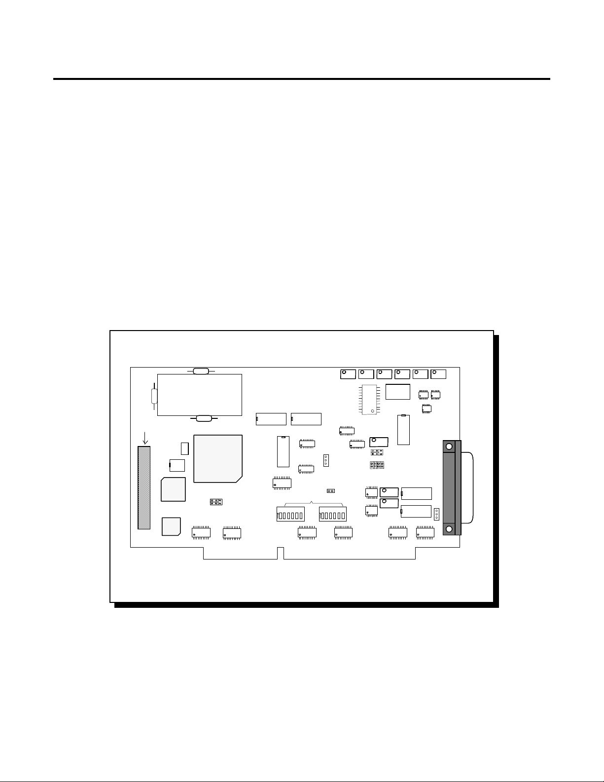
The component layout diagram for the DAQ-1200 series circuit board is depicted in Figure
1-1.
DAQ-1200
DC/DC
AD7892
Auxiliary I/O
FIFO
FPGA3042
FIFO
FIFO
J3
PGA
J4
J5
8255A
8254
J2
SW1
Base I/O Addres s
1234
56
1234
J1
56
D/A
SW2
D/A
Figure 1-1. Component Layout Diagram
J6
Page 9
1.1 Analog Input Features
The DAQ-1201/1202 supports 8 differential (positive and negative connections) or 16 single
DAQ-1200 Series Users Manual 9
ended analog input signals. The 16 single ended channels can be further expanded to 256
channels with the addition of an external analog multiplexer card and by using four of the
eight digital I/O lines for multiplexing control. Selection of either single ended or differential
analog inputs is software programmabl e. The DA Q-1201/1202 contains one high speed 12- bit
analog-to-digital converter (ADC) which can be configured to receive analog input voltages
within the range of -10v to +10V.
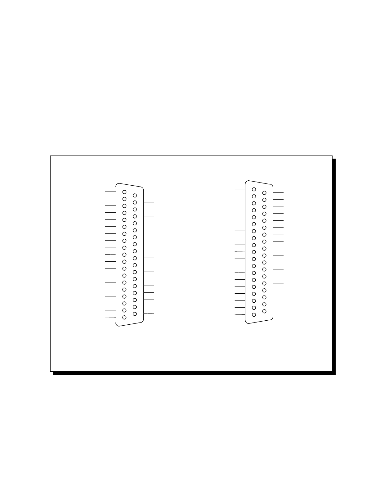
1.1.1 D37 Connector Pin Diagrams
Analog I/O connections are made through D37 connectors as shown in Figure 1-2.
Analog GND
-CH0
-CH1
-CH2
-CH3
-CH4
-CH5
-CH6
-CH7
DA0 Ref/SSH Out
DA 0 Out
Vref (-5V)
Power GND
IP1/GS0
IP3/GS1
OP1/CHS1
OP3/CHS3
Timer0 Out/-15V
+5V
Main I/O Connector
19
18
17
16
15
14
13
12
11
10
9
8
7
6
5
4
3
2
1
37
36
35
34
33
32
31
30
29
28
27
26
25
24
23
22
21
20
+CH0
+CH1
+CH2
+CH3
+CH4
+CH5
+CH6
+CH7
Analog GND
Analog GND
DA1 Out
DA1 Ref
IP0/Ext TTL Tr i g / Timer 1 C l k
IP2/Ti mer0 GATE
OP0/CHS0
OP2/CHS2
Timer0 Clk/+15V
Timer2 Out
Auxiliary Connector
DIG COM
+5V
DIG COM
DIG COM
DIG COM
DIG COM
PB0
PB1
PB2
PB3
PB4
PB5
PB6
PB7
19
18
17
16
15
14
13
12
11
10
9
8
7
6
5
4
3
2
1
37
36
35
34
33
32
31
30
29
28
27
26
25
24
23
22
21
20
OP=Digital Output (4 bit port) DA=D/A Channel PA=Port A (bit 0-7)
CHS=Channel Select GS=Gain Select PB=Port B (bit 0-7)
IP=Digital Input
PC=Port C (bit 0-7)
PA0
PA1
PA2
PA3
PA4
PA5
PA6
PA7
PC0
PC1
PC2
PC3
PC4
PC5
PC6
PC7
DIG COM
+5V
Figure 1-2. D37 Pin Diagrams
Pins 11 through 18 and pins 30 through 37 are the available analog input channels. For
differential input, the eight available channels are numbered 0 through 7 and each channel
consists of one positive input (+CHx) and one negative input (-CHx). In single-ended
operation, the available channels are numbered 0 through 15. Inputs +CH0 through +CH7
correspond to channels 0 through 7 respectively. Inputs -CH0 through -CH7 correspond to
channels 8 through 15 respectively.
Page 10

1.1.2 Gain Selection Ranges
The DAQ-1201 provides gains of 1, 10, 100 and 1000 versus the DAQ-1202, which provides
DAQ-1200 Series Users Manual 10
gains of 1, 2, 4 and 8. Tables 1-1 and 1-2 show the analog input unipolar and bipolar voltage
ranges for the respective gain range.
DAQ-1202 DAQ-1201
GainInput RangeGainInput Range
10 to 10V10 to 10V
20 to 5V100 to 1V
40 to 2.5V1000 to 100mV
80 to 1.25V1,0000 to 10mV
Table 1-1. Unipolar Analog Input Voltage Ranges
For a gain setting of 1, the 12-bi t resolution (4096 count) provides a least signif icant bit (LSB)
value of 2.44 mV in the 0 to +10V range.
DAQ-1202 DAQ-1201
GainInput RangeGainInput Range
1-10V to +10V1-10V to +10V
2-5 V to +5 V10-1 V to +1V
4-2.5 V to +2.5V100-100mV to +100mV
8-1.25 V to +1.25V1,000-10mV to +10mV
Table 1-2. Bipolar Analog Input Voltage Ranges
For a gain setting of 1, the 12-bi t resolution (4096 count) provides a least signif icant bit (LSB)
value of 4.88mV in the ±10V range.
1.1.3 Source and Trigger Mode for Analog-to-Digital Conversions
Upon initial power up, the DAQ-1201/1202 is in idle mode and no conversions are performed.
Conversions begin upon receiving a trigger. Three types of triggers are available: internal
trigger, external trigger and analog trigger. The internal trigger is initiated by a software
program, whereas the external trigger is connected through hardware. The analog trigger
occurs when the input signal exceeds a preset level set by the user. The preset level or
"threshold voltage" is generated by the output of the second D/A converter. A comparator
circuit sets of f the analog tr igger when the input signal rises above threshold voltag e. When
the trigger is initiated, the ADC immediately converts the analog signal into 12-bit digital data
which is stored in the data FIFO (First In First Out) register. In addition to varied triggering
sources, a triggering mode is available to select whether conversions and channel scans are
completed only once or multiple times. Trigger source and trigger mode types are software
selectable.
Page 11

Triggering functions are summarized as follows:
DAQ-1200 Series Users Manual 11
(a) Trigger source :
y
Software trigger
y
External TTL trigger on falling or rising edge
y
External analog trigger with low to high or high to low transition
For the external TTL trigger, the default trigger pin on the main D37 connector is pin 25
(IP0/Trig).
(b) Trigger mode:
y
Single -- one scan/conversion for each trigger
y
Continuous -- continuous scanning/conversions for one trigger
1.1.4 Scan List (Scan FIFO)
The DAQ-1201/1202 scan list function performs high speed A/D conversions from channel to
channel. A scan FIFO regi ster is provided with a depth of 512 points that contains the channel
scan sequence and gain information. The scan FIFO must be programmed according to the
scan sequence desired . Scan sequence order can be random with channels configured in any
sequence desired. Channel sequences can also be repeated in an arbitrary order.
Each FIFO locati on occupies two bytes with the fi rst byte (low byte) storing the sequence for
extended channels beyond the on board 16 channels and their associated gain information.
The second byte (high byte) stores the sequence of on board channels and their gain
information. A bit in each location i n the FIFO (bit 7 of the high byte) is used to identify the
beginning channel . This bit, whi ch signals the completion of one scan cycl e, is registered as a
logic 1 for the beginning sequence and logic 0 for the others. When the scan list function is
initiated, A/D conversion begins from the start channel. After the conversion is completed,
digitized data is entered into the data FIFO and the board selects the next location to repeat
the same task. This process continues until the stop channel is reached. For single trigger
mode, it scans once and then stops. I n continuous mode, scanning continues at a speed set by
the sampling rate until the desired number of scan times is reached.
The scan FIFO is programmable for up to a 256 channel scan list with an individual gain
setting for each channel. The scan speed from channel to channel is 2.7µs. This speed is
sufficient for the ampli fier settling time of all gain selection values except 1000. Wi th a gain
setting of 1000 for the DAQ-1201, it requires 10µs for the amplifier to settle down. By
programming the scan FIFO to repeat the same channel scan four times for each channel , the
scan speed can be slowed to 10.8µs.
Page 12

1.1.5 Sampling Rate
DAQ-1200 Series Users Manual 12
When digitizing the analog signal, one user selectable parameter is the sampling rate which
determines how fast the analog signal is digitized. The minimum sampling rate must be at
least two times the input signal frequency to accurately recover digitized data from the
original anal og input signal. The max imum sampling rate of the DA Q-1201/1202 is 400 kHz
and is derived from the on board 8254 chip which has three 16-bit counter/timers. The clock
input to Timer1 is 10MHz. Timer1 and Timer2 are cascaded to generate the sampling rate
pulse which in turn tr iggers A/D conversion. T he counting range of both timers is fr om 2 to
65535. Sampling period is computed as follows:
Sampling period = (Timer1 data) x (Timer2 data) x (100 nanoseconds)
The sampling rate in hertz is the i nverse of the sampl ing peri od. To set the highest sampli ng
rate of 400 kHz, the sampling period must be ms, or 2.5µs.
1
400
Timer1 and Timer2 values are calculated as follows:
(Timer1 data) x (Timer2 data) = 2500100
= 25
Timer1 and Timer2 data should be an integer ranging from 2 to 65535.
1.1.6 Simultaneous Sample Hold (SSH)
SSH uses a TTL signal which is logic high in "sample" mode and logic low in "hold" mode.
SSH is set to sample mode be fore the conversi on of the fir st channel in the scan list a nd then
switches to hold mode after the first conversion is completed. Hold mode remains set until the
last channel in the scan l ist is converted. Due to the settling time of the Programmable Gain
Amplifier (PGA), which is about 2µS for gain settings less than 1000, the first channel is not
perfectly si multaneous wi th the rest of the channels in the scan list. T his can be over come by
programming the first channel twice in the scan list and discar ding the non-simulta neous data
while processing.
If the need arises to write code for access to the DAQ-1201/1202 registers independent of
DAQDRIVE®, complete the following actions to implement SSH:
1. Set bit D6 of the even byte (low byte) in the scan FIFO to 1 for the first channel in the
scan list.
2. Set bit D6 of the even byte (low byte) in the scan FIFO to 0 for rest of the channels in
the scan list.
Page 13

1.1.7 Data FIFO
DAQ-1200 Series Users Manual 13
DAQ-1201/1202 uses a data FIFO register between the output of the ADC and the ISA bus to
buffer data from the ADC output. Unlike conventional A/D boards where the di gitized data
output is fetched directly to the PC memory, the output data from the ADC is fed into the
FIFO first for temporary storage. The length of the FIFO register is 1024 sampling points and
the register circuit provides hardware flags for half full, full and empty signals. Utilizing these
signals, the b oard ca n genera te an inter rupt to the PC when the FIFO i s ha lf f ull . Once the PC
interrupt is complete, the interrupt service routine program uses the "MOVE STRING"
instruction to move the FIFO da ta directly in to PC memory at a very high speed. In this case,
it only interrupts the PC every 512 samples and thereby improves the speed of operation. In
Windows appl ications, the latency of the inte rrupt d oes not effect the i ntegr ity of the di gi tized
data as it continues into the FIFO. The status register (see Chapter 5, Table 1-5: Address map)
provides information about FIFO empty, half full and full conditions.
1.1.8 Direct Memory Access (DMA) Data Transfer
Another way of transferring digitized data from the A/D converter to memory is DMA
transfer. D MA operation is accompli shed by transf erring the data at the I/O l ocation directl y
to the PC memory by-passing the CPU. The DAQ-1201/1202 i mplements this DMA transfer
utilizing an AT style ISA bus with 8-bit DMA transfer channels (1,2,3) and 16-bit transfer
channels (5,6,7). The DAQ-1201/1202 employs word transfer to improve its efficiency and
allows for software programmable selection of the DMA channel. Proceeding any DMA
transfer, the PC DMA controller must be programmed with mode of operation, number of
words transferred and memory location. After programming the controller, then the FPGA
will initiate a DMA request to start the operation. When the data transfer is complete, a
terminal count pulse is generated by the controller and is used as an interrupt to inform the
PC at the completion of data transfer.
The DMA contr olle r only handl es d ata tra nsfer of 64 K points (one se gment) . Be yond that, the
controller must be reprogrammed again. When acquiring data beyond 64K points with a fast
pace sampling rate, data points can be missed during reprogramming of the DMA controller.
The DAQ-1201/1202 remedies this by utilizing two DMA channels. When one channel is
performing DMA operations, the other channel can be reprogrammed by the user. At the
terminal count, operation then switches to the reprogrammed channel and the completed
DMA channel is then available for reprogramming. This dual channel operation guarantees
the integrity of the data stream and is limited only by the memory size of the PC.
1.2 Analog Output Features
In addition to the analog input channels, the DAQ-1201/1202 contains two analog output
channels. Each channel has its own 12-bit digital-to-analog converter (DAC). The analog
outputs are buffe r ed and capable of 1 mA of output current. Th e output vol ta ge range for each
channel is jumper selectable as unipolar or bipolar. The 12-bit resolution provides a LSB value
of 4.88mV on the ±10V range and 2.44mV in the 0 to +10V range.
Page 14

Both channels use multiplying DACs which require a reference voltage input in addition to
DAQ-1200 Series Users Manual 14
the 12-bit digital values. The DAQ1201/1202 provides an internal reference voltage while an
external reference voltage can also be supplied via jumper configuration.
Analog output has two modes of operation: I/O write operation and DMA write operation.
DMA write oper ation for analog output performs faster than I/O operation. Opposi te to the
DMA analog i nput function, DMA for analog output can transfer data in PC memory to the
DAC port at a pace set by the timer. Once again dual channel configuration is available for
DMA output operation which provides for data transfer beyond 64K points. Note that only
one port can be operating at a time.
1.3 Digital I/O
The DAQ-1201/1202 has 32 digital I/O lines. Of the 32 lines, 8 of them can be accessed
through the main D37 connector. There are 4 inputs: IP0 through IP3, and 4 outputs: OP0
through OP3, ( refer to F igure 1- 3 for pi n locations) . The remainin g 24 I/O lin es are g enerated
by an 8255 programmable peripheral interface chip and are accessed through the auxiliary
D37 connector. The 8255 has three ports (A, B and C) and one control register. Any port can b e
programmed as in put or output. Ports A and B ar e 8 bit I /O por ts whil e port C can be f urther
divided into two 4-bi t I/O ports. T he 8255 has three modes of operation whi ch are d etermi ned
by values wr itten into the control regi ster. Mode 0 i s for basic input/output config uration in
which the output port is l atched and the input por t is not. Mode 1 employs Port A or B a s the
data port while using Port C for handshake, interrupt, and digital I/O lines. Mode 2 uses Port
A as the bi-directional data port with Port B and C as control and digital I/O lines. For a
detailed functional description, the reader is referred to the Intel® 8255 data manual.
1.4 Counter / Timer
The 8254 counter/timer chip on the DAQ-1201/1202 provides three 16-bit counter/timer
channels for time-related applications. Timer1 and Timer2 are cascaded together with an
input clock of 10 MHz and the output of Ti mer 2 is used as the sampl i ng r ate cl ock f or the A /D
converter. Three terminals for Timer0 are available to the user via the main I/O D37
connector. The three terminals are Pin 2 (Timer0 output), Pin 21 (Timer0 Clk) and Pin 24
(Timer0 Ga te). The gate te rminal should b e logic high in order for the counter to f unction. If
gate is held at logic low, the counter is disabled.
Page 15

1.5 Interrupts
DAQ-1200 Series Users Manual 15
The DAQ-1201/1202 supports AT style ISA bus interrupts which includes IRQ 2-7, 10-12 and
14-15. The selection of inter rupts is softwa re programmabl e through the reg ister setting of the
FPGA. Any interrupt conflict can be conveniently resolved by moving the selection to another
available line without opening the computer case. There are five interrupt sources from
DAQ-1201/1202:
y
End of scan
y
Data FIFO Half Full
y
Data FIFO Full
y
Timer0
y
Terminal count
The end of scan interrupt is normally used in conjunction with single trigger mode. After the
scan list is completed , the end of scan generates an interr upt to inform the computer to fetch
the data.
The data FIFO half full interrupt is used during continuous trigger mode. When the FIFO is
half full, i t interrupts the PC to fetch at least 512 sample points. This interrupt is works well in
the Windows environment because of interrupt latency problems inherent in the Windows
operating system.
The data FIFO full interrupt is not recommended for applications unless the interrupt routine
is executed promptly before the next data points are accepted. Otherwise an overflow can
occur and data may be lost.
Timer0 in terrupt is used in conjunction with the external ti mer at the main D37 connector. The
external cl ock pulses are connected to the Ti mer0 clk input (pi n 21) and the output of Timer 0
can be used as an interrupt source. When the user must interrupt the PC at a certain time
interval, timer0 can be programmed to meet the requirement.
Terminal count interrupt occurs at the completion of DMA transfer. The terminal count
interrupt informs the user that DMA transfer has finished.
Page 16

1.6 Software Support
DAQ-1200 Series Users Manual 16
Software drivers are provided to support various programming languages like Microsoft
C/C++, Borland C/C++, QuickBasic, Visual Basic for DOS and Turbo Pascal. A Dynamic
Link Library (DLL) is provided for numerous programming languages under Microsoft
Windows as well as Visual Basic Controls. Software support is available on the Omega
"DaqSuite" compact disk in the following categories:
1. DAQDRIVE® Software driver
2. DaqEZ™ Data Acquisition Package
3. VISUALDAQ ® Data Acquisition Package
DAQDRIVE is a low level generic driver consisting of a set of user commands that act as a
library routine for all Quatech data acquisition boards. Programs written for the
DAQ-1201/1202 can be ported to other boards i n the event the user decides to change boards
in the fu ture. DAQDRIVE is avai lable for Wi ndow DLLs and the MS-DOS environment. In
the case of Visual Basic applications, Omega provides VISUALDAQ®. Because of it's user
friendly nature, this software is very practical for interaction with data acquisition boards and
for creating graphic presentations.
Omega also provides driver support for third party data acquisition packages such as
TestPoint® (Capital Equipment Corporation) and LabVIEW® (National Instruments). These
packages allow the user to create custom test, measurement and data acquisition applications.
1.7 Power Requirements
The DAQ-1201/1202 is powered di rectly by the +5V and +12V power source provided b y the
computer bus.
Page 17

1.8 Applications
DAQ-1200 Series Users Manual 17
The DAQ-1201/1202 performs the following functions: analog input (A/D), analog output
(D/A), digital I/O and timer/counter functions. Typical applications for each function are
listed as follows:
A/D conversion converts analog voltage into digital information, which enables the computer
to process or to store the signals. Typical appl ications are sensor or transd ucer measurement,
wave form acquisition/analysis and data storage. (Most sensor/transducer measurements
require signal conditioning prior to measurement by an A/D converter. Omega SignalPro
Series signal conditioning modules offer a complete solution for data acquisition using sensors
or transducers).
D/A conversion is the opposite of A/D conversion. This operation converts digital
information to analog voltage. Typical applications are process control and function/pulse
train generation.
The digital input function is useful in applications such as contact closure or switch status
monitoring. The digital output function is useful for relay control and industrial on/off
control.
A timer/counter is typical ly used for event counting a nd pulse generati on. It can also be used
for frequency, period or pulse measurement.
Page 18

1.9 DAQ-1201/1202 Specifications
256 Samples
Size of Scan List
Gain Ranges:
Twos complement
Output Data Code
-10V to +10V
Input Ranges
8 differential, 16 single ended
Channels
400 kHz
Maximum Sampling Rate
Analog Input
Straight Binary
Output Data Coding
0 - 5V, 0 - 10V, ±5V, ±10V
Output Ranges
2
Channels
Analog Output
82C54
Type
82C55A
Type
24 bits
I/O
(24 bits on Auxiliary Connector
)
Digital I/O
DAQ-1200 Series Users Manual 18
expandable to 256
Model 1201
Model 1202
Surge Protection up to
1, 10, 100, 1000
1, 2, 4, 8
1 M ohmInput Impedance
50pAInput Bias Current
±20 V
12-bitResolution
Successive ApproximationConversion type
1.6 µsConversion Time
12-bitResolution
(8 bits on main D37 Connector)Digital I/O
Timer/Counter
4Output Bits
4Input Bits
3, downNumber of Counters
Page 19

120 mA typ, 160 mA max
+12V DC
800 mA typ, 1000 mA max
+5V DC
Power Requirements
0-95%Humidity
3-7, 9-12, 14, 15
Interrupt Level
0 - 70° C
Operating Temperature
Environments
DAQ-1200 Series Users Manual 19
8.5 in x 4.8 inDimensions
Page 20

2 Hardware Configuration and Initial Setup
This section describes how to unpack and configure the DAQ-1200 series circuit board.
DAQ-1200 Series Users Manual 20
2.1 Unpacking
The DAQ-1201/1202 is packed in an anti-static bag to avoid possible damage to the
electrostatic d ischarge se nsitive components on the b oard. B efore removing the product from
it's protective bag, touch both the bag and the computer chassis to establish grounding. If
available, utilize a static free work station to unpack the DAQ-1201/1202. Once grounding has
been established, remove the board from it's packaging and inspect it for signs of damage.
2.2 Auxiliary Connector Cable
The DAQ-1201/1202 auxiliary I/O connector can be accessed via a PC expansion slot by
attaching the cable assembly included with the product.
40 pin
Male
Connector
Connector
Auxiliary I/O
Main I /O
40 pin
DAQ-1201/1202
Female
Cable Assembly: P/N 920-0048-01A
Figure 2-1. Auxiliary Connector Cable
D37 Male
Connector
Page 21

2.3 Configuring the DAQ-1201/1202
The user must decide the appropriate configuration for the DAQ-1201/1202 board depending
DAQ-1200 Series Users Manual 21
on the application. The DIP switch settings for SW1 and SW2 and the jumper settings for J2,
J3, J4, J5 and J6 must be selected before installing the board in the computer. While software
programmable configurations can be done later, the following items are jumper or switch
configurable and must be decided before installing into the PC:
1. I/O base address selection
2. D/A voltage reference, bipolar/unipolar output range.
3. Internal/external clock source for Timer 0
4. Clock source for A/D converter
5. Timer0 out/ -15 v and Timer0 Clk/+15v selection
2.3.1 I/O Base Address Selection
Each board in the PC must have a uni que input/output a ddr ess. No tw o b oard s can shar e the
same address. Similar to a mailbox, the PC processor sends data to or fetches da ta from this
address. Some of the I /O locations are pre-assigned standard d efault locati ons such as COM1
(3F8H) and COM2 (2F8H). Printer port locati ons such as LTP1 are also fixed. T he I/O base
address for most other hardware is flexible and can be any value as long as that space is not
occupied. Figure 2-2 shows the location of SW1 and SW2, the I/O base address selection
switches.
Auxiliary I/O
8255A
8254
DAQ-1200
DC/DC
AD7892
FIFO
FIFO
Base I/O Addres s
1234
56
A
987654
J3
J1
1234
56
SW2
234561
AAAAA
PGA
J4
J5
D/A
D/A
SW2
ON
FPGA3042
J2
1
SW1
3456
2
A
AAAA
14 13 12 11 10
FIFO
SW1
Figure 2-2. I/O Base Address Selection Switches
J6
Page 22

The I/O base address of the DAQ-1201/1202 is set using two DIP switches SW1 and SW2.
DAQ-1200 Series Users Manual 22
When a switch bit is in the "ON" position, then the corresponding address line is logic 0.
When a switch bit is in the "OFF" position, then the corresponding address line is logic 1. The
I/O base address can be selected from 0000H to 7FF0H with a 0010H interval. The upper limit
of 7FF0H implies that the address has only 15 lines and the most significant bit A15 is always
0. Switches SW1 and SW2 select address lines A14 through A4. Since the board encompasses
16 register locations which require 4 address lines, (A3, A2, A1 and A0), only A14 through A4
address lines are used for base address decoding. Figure 2-3 shows several switch
configurati ons and the I/O base addresses they repr esent. The factory defa ult address setting
is 300H.
Do n't care
xxxxx
123456
O
N
SW1
xxxxxx
123456
O
N
SW2
03 10
00000 11 1000
123456
O
N
Example1: Base I/O Address = 0310H
123456
O
N
6A D0
11010 10 1110
123456
O
N
123456
O
N
Example 2: Base I/O Address = 6AD0H
0000
Bit=0 Bit=1
xxxx Hex
0000 : 0
0001 : 1
0010 : 2
0011 : 3
0100 : 4
0101 : 5
0110 : 6
0111 : 7
1000 : 8
1001 : 9
1010 : A
1011 : B
1100 : C
1101 : D
1110 : E
1111 : F
Figure 2-3. I/O Base Address Selection
Page 23

2.3.2 D/A Voltage Reference
The digital to analog converter in the DAQ-1201/1202 uses multiplying DAC AD7545. This
DAQ-1200 Series Users Manual 23
chip requires a reference voltage connection. There are two reference voltages selections
available: one is the internal power supply +5 vdc reference voltage and the other is an
external input. Figure 2-4 illustrates internal/external reference voltage selection for D/A
channels DA0 and DA1. Connect J4 to the applicable pins for the desired reference voltage:
DA0 DA1
External reference Pins 2 & 3 Pins 5 & 6
Internal reference Pins 1 & 2 Pins 4 & 5
DAQ-1200
DC/DC
AD7892
Auxiliary I/O
FIFO
FPGA3042
FIFO
FIFO
J3
PGA
J4
J5
8255A
8254
J2
SW1
Base I/O Addres s
1234
56
DA1
DA0
J1
1234
4 5 6
1 2 3
SW2
56
Internal Ref erence
External Reference
J4
Figure 2-4. D/A Voltage Reference Jumper
D/A
D/A
J6
Page 24

2.3.3 Bipolar/Unipolar Output Range Selection
Each D/A output has an option of either Unipolar or Bipolar connections. In addition, the
DAQ-1200 Series Users Manual 24
output voltage range can also be selected. Unipolar or bipolar output selection is made by
either connecting or not connecting jumper J5 as applicable for the desired output result.
Tables 2-1 and 2-2 list the combinations of jumper confi gurations for available voltage range
selections. The location and configuration options for jumper J5 are shown in Figure 2-5.
D/A0 output voltage Pins 2 & 6Pins 1 & 5
-5V to +5V, bipolarConnectConnect
-10V to +10V, bipolarOpenConnect
0 to +5V, unipolarConnectOpen
0 to +10V, unipolarOpenOpen
Table 2-1. DA0 Output Voltage Ranges
D/A1 output voltage Pins 4 & 8Pins 3 & 7
-5V to +5V, bipolarConnectConnect
-10V to +10V, bipolarOpenConnect
0 to +5V, unipolarConnectOpen
0 to +10V, unipolarOpenOpen
Table 2-2. DA1 Output Voltage Ranges
Auxiliary I/O
8255A
8254
DC/DC
FPGA3042
Connect: bipolar
Open: unipolar
Connect: 5v range
Open: 10v range
J2
DAQ-1200
FIFO
SW1
DA0 DA1
J5
FIFO
Base I/O Addres s
1234
5678
1234
FIFO
J3
1234
56
Connect: 5v range
Open: 10v range
Connect: bipolar
Open: unipolar
J1
56
SW2
D/A
D/A
AD7892
PGA
J4
J5
J6
Figure 2-5. Bipolar/Unipolar Output Range Selection Jumper
Page 25

2.3.4 Timer0 Internal/External Clock Selection
The timer0 connection is used f or timing or counting applicati ons. Jumper block J2, shown in
DAQ-1200 Series Users Manual 25
Figure 2- 6, is used to sele ct the internal or external clock w hich connects to the clock input of
timer0 at pin 21 on the main I/O D37 conne ctor. When configured for an external input, the
timer/counter can be used for pulse counting an external event. Configure jumper J2 as
necessary for the desired clock input:
Internal 10 MHz clock Jumper pins 1 & 2 on J2
External clock Jumper pins 2 & 3 on J2
DAQ-1200
DC/DC
AD7892
Auxiliary I/O
FIFO
FPGA3042
FIFO
FIFO
J3
PGA
J4
J5
1234
J1
56
SW2
D/A
D/A
J6
8255A
8254
J2
J2
SW1
46
5
13
2
Base I/O Addres s
1234
56
Internal 10MHz Clock (pins 1/2 and 4/5)
External Clock (pins 2/3 and 5/6)
ADC Clock Input (Timer1in/Timer2 out)
Timer0 Clock Input
Figure 2-6. Internal/External Clock Selection Jumper
2.3.5 ADC Clock Source
Timer1 and timer2 are cascaded together and the output of timer2 is used as the sampling
clock for the ADC. The sampling rate can be changed by writing different values into timer1
and timer2 . The clock input to timer1 has two diff erent sources: an inter nal 10 MHz clock and
an external clock tha t can be connected at pin 25 on the main I/O D 37 connector. Confi gure
jumper J2 as necessary for the desired clock input, (refer to Figure 2-6):
Internal 10 MHz clock Jumper pins 4 & 5 on J2
External clock Jumper pins 5 & 6 on J2
Page 26

2.3.6 Timer0 and +15v/-15v Selection
Jumper pins 2 & 3
Jumper pins 1 & 2
+15 v and -15 v
Jumper pins 1 & 2
Jumper pins 2 & 3
Timer0 output
DAQ-1200 Series Users Manual 26
On the main D37 connector, pin 21 and pi n 2 have d iff erent functi onal connections d ependi ng
on the config ur ati on of jumpers J 3 and J6. I f the user requir es timer/counter applications, then
pin 2 and pin 21 on the main I/O D37 connector can be configured for timer0 output and
timer0 input re spectively. If the use r does not require timer/counter connections but has use
for the +15v or -15v output at the D37 connector, then J3 and J6 can be configured for this
option. Figure 2-7 shows the location and configuration options for J3 and J6.
J6J3Pin 2 and Pin 21
Main I/O D37 connector
Timer0 Clk input
Table 2-3. Jumper J3 and J6 Configuration Options
DAQ-1200
DC/DC
AD7892
Auxiliary I/O
FIFO
FPGA3042
FIFO
FIFO
J3
PGA
J4
J5
1234
J1
56
D/A
SW2
D/A
8255A
8254
J2
SW1
Base I/O Addres s
1234
56
J6
J3
3
2
1
Pin 21 is Timer0 Clk
Pin 21 is +15V
1
2
3
Pin 2 is Timer0
Output
Pin 2 is -15V
Figure 2-7. Timer0 and +15v/-15v Selection Jumpers
J6
Page 27

2.3.7 Simultaneous Sample and Hold (SSH)
DAQ-1200 Series Users Manual 27
The SSH output signal shares the pin 10 of main I/O D37 connector with the external
reference of DA channel 0. Jumper J1 is used to enable or disable SSH. With J1 installed SSH is
operational, with J1 removed SSH is disabled. Note that if SSH is enabled, the DA0 reference
jumper J4 must be configured for internal reference operation as depicted in Figure 2-8.
DAQ - 1200
4 5 6
DAC1
SW2
DAC0
1 2 3
FPGA 3042
SSH
SW1
1234
J1
Base I/O Address
1234
56
SSH
56
Figure 2-8. Simultaneous Sample and Hold Jumper
Internal Reference
External Reference
J4
Pin 10 of D37
DAC0 Ref/SSH
Page 28

2.4 Installation under Windows 95/98®
DAQ-1200 Series Users Manual 28
Windows 95/98 maintains a registry of all known hardware installed in a computer. Inside
this hardware r e gistry Windows keeps tr ack of all system resources such as I /O l ocati ons, I RQ
levels and DMA channels. The "Add New Hardware Wizard" utility in Windows 95/98 was
designed to add new hardware and update this registry.
An "INF" file is included with the DAQ-1201/1202 to allow easy configuration in the
Windows environment . Windows uses the "INF" file to determine the system resources
required by the DAQ-1201/1202, searches for available resources to fill the boards
requirements and then updates the hardware registry with an entry that allocates these
resources.
Windows will not automatically configure the DAQ-1201/1202. The user is required to
manually configure the hardware to match the resources that Windows allocates to the
DAQ-1201/1202. Another option is to use the "Device Manager" i n Windows to change the
system resources allocated to match the configuration of the hardware.
2.4.1 Using the "Add New Hardware Wizard"
The following instructions provide step-by-step instructions for installing the DAQ-1201/1202
with Windows 95/98 b y usi ng the "Add New H ard ware Wizard". Sel ect Start|Help f rom the
Windows start bar for additional information on this utility.
1. Start the Add New Hardware Wizard utility. The icon for this utility is located in
the Windows 95/98 control panel.
2. A dialog box will appear which initiates the "Add New Hardware Wizard" utility.
Select the "Next" button to continue.
3. An option box a ppears al lowi ng the choi ce of havi ng Wi ndows a utomatical ly d etect
the new hardware. Select the "No" option. The dialog in the box recommends
selecting the "Yes" option, but unless the hardware is installed with standard I/O
and IRQ levels, this option will fail. Select the "Next" button to continue.
4. A hardw are type list box shoul d appe ar. Sele ct the "Other Devices" type on the l ist
and then select the "Next" button to continue.
5. A list b ox opens wi th Manufacture rs on the lef t and the a ssociated b oard Model s on
the right. Select the "Have Disk" button.
6. An "Install From Disk" dialog box should pop open. Insert the customer CD-ROM
with the DAQ-1201/1202 INF files on it, select the correct drive letter and then
select the "OK" button. Wind ows 95 automati call y br owses the root di rector y for an
INF file that defines configurations for the circuit board. If no INF files are found,
click the " Browse" button and sea rch the Wi n95/98 sub d irectory on the install ation
CD for the file named DAQPCARD.inf. (The file name is not required. After finding
the directory containing the INF files, Windows 95/98 will choose the correct file).
Page 29

7. Your computer should read the INF file and display a list of Omega data acquisition
board models supported by Windows 95/98. Select the DAQ-1201 or DAQ-1202
DAQ-1200 Series Users Manual 29
model name from the list and select the "Next" button to continue.
8. A dialog box will appear with an unused I/O range and IRQ resources that
Windows has f ound avai l ab l e i n the registry. Wi nd ow s has assi g ned these resources
to the DAQ-1201/DAQ-1202. Review these settings carefully before proceeding.
Either take notes of the resources being allocated to the new hardware or have
Windows 95/98 print a copy. The DAQ-1201/1202 must then be manually
configured to match these resources. Windows will not automatically configure the
DAQ-1201/1202.
9. Another dialog box will open when the installation is complete. Select the "Finish"
button to end the software installation.
10. Windows 95/98 will then instruct the user to shut down the computer and install
the hardware . Select the "Yes" button to shut down the computer . When Window s
95/98 sends the "safe" message, then power down the computer.
11. Either manually configure the DAQ-1201/1202 to match the resources allocated by
Windows or use the "Devi ce Manager" in Windows 95/98 to change the previ ously
allocated system resources to match your preferences (see section 2.4.2: "Changing
Resources with Device Manager").
Page 30

2.4.2 Changing Resources with Device Manager
The following instructions provide step-by-step instructions on viewing and changing
DAQ-1200 Series Users Manual 30
resources of the DAQ-1201/1202 in Windows 95/98 using the "Device Manager" utility. Select
Start|Help from within Windows 95/98 for additional information on this utility.
1. Double click the "System" icon inside the Control Panel folder. This opens up the
System Properties box.
2. Select the "Device Manager" tab located at the top of the System Properties box.
This lists all hardware devices listed inside the Windows 95 registry. Additional
information is available on any of these devices by clicking on the device name and
then selecting the "Properties" button.
3. Double click the device group "Data_Acquisition". The DAQ-1201/1202 model
name should appear on the list of hardware.
4. Double click the DAQ-1201/1202 model name and a properties box should open.
5. Click the "Resources" tab located along the top of the properties box. Confirm
Windows has allocated resources for the DAQ-1201/1202 that match the board's
hardware confi guration. To modify any of the resource settings select the resource
name and click the "Change Setting" button. Sele ct "Cancel" to exi t without maki ng
changes.
6. When the "Change Settings" button is selected, an "Edit Resource" window will
open. Insid e thi s wi ndow, cli ck on the up/dow n arrow s to the rig ht of the resour ce
value. This scrolls through all of the allowable resources for your hardware. Note
the Conflict Inf ormation at the bottom of the window . Do not sele ct a resource that
causes a conflict with any other installed hardware. Select "OK" to save your
changes or "Cancel" to abort changes.
7. You are required to manually confi gure the DAQ-1201/1202 to match the resources
allocated by Windows 95/98.
Page 31

3 Field Wiring
Before completing any installation or connection, ensure power is not applied to the computer
DAQ-1200 Series Users Manual 31
or external circuits. Install the DAQ-1201/1202 as directed by the procedures in Chapter 2:
Hardware Configuration and Initial Setup. The main I/O D37 connector on back of the PC
contains all the analog input and output signal pins. The auxiliary connector is used for
digital I/O connection. Both connectors and Omega cables are Keithley MetroByte
DAS-1600 compatible.
3.1 I/O Terminal Connection
The user can connect either one or both I/O connectors on the DAQ-1201/1202 to the external
UIO-37 screw terminal block shown in Figure 3-1. The UIO-37 has 37 numbered screw
terminals that correspond one to one to the pins on both the main I/O and auxiliary D37
connectors on the DAQ-1201/1202. The UIO-37 provid es a convenient connection for external
wiring and is avai l abl e w i th either a male or female D37 connector. Wire gage 16 through 28 is
recommended for screw terminal connections.
D37 Connector (Male or Female available)
TM
Screw Terminal Connections
Ground
Figure 3-1. UIO-37 Screw Terminal Block
Page 32

The UIO-37 is connected to the PC using the Omeg a CP-DAQ D37 f emale to mal e 3 foot cable
DAQ-1200 Series Users Manual 32
as shown in Figure 3-2. The CP-DAQ cable male end connects to the UIO-37 female D37
connector and the female end connects to the main I/O and auxiliary connectors on the
DAQ-1201/1202.
Computer
Main
CP-DAQ
Auxiliary
19
18
19
18
3
2
1
3
2
1
UIO-37
19
CP-DAQ
D37 female to male
3 foot cable
1
18
19
18
3
2
3
2
1
UIO-37
Figure 3-2. Connection of UIO-37 Terminal Blocks to DAQ-1200 Series Connectors
Page 33

3.2 Analog Input Field Wiring
DAQ-1200 Series Users Manual 33
3.2.1 Single Ended Input
The analog input signals can have either single ended or differential inputs. Figure 3-3
illustrates field wiring for single ended inputs. There are 16 single ended channels available.
Main I/O D37 connector inputs +CH0 through +CH7 correspond to channels 0 through 7
respectively. Inputs -CH0 through -CH7 correspond to channels 8 through 15 respectively.
Single ended signals usually consist of a positive input signal wire (+) and a negative input
signal wire (-) . Connect the (+) wire to the desired input channel terminal and the (-) wire to
the UIO-37 analog ground terminals 19 and 29.
If a high electrical noise environment exists, individual shielded wiring is recommended.
Keep the signal lines as far from the power line as possib l e and never bund l e si gnal cabl es and
high current or voltage cables in the same harness. High electric field intensity may
deteriorate or interfere with the signal being measured.
DAQ-1201/1202
()
37
+CH0 (analog channel 0)
18
-CH0 (analog channel 8)
+CH1 (analog channel 1)
36
17
-CH1 (analog channel 9)
+CH7 (analog channel 7)
30
11
-CH7 (analog channel 15)
25
IP0/EXT TTL TRIG
19
29
+
Vin8
+
Vin9
+
Vin15
DAQ-1200
DC/DC
AD7892
FIFO
PGA
FIFO
J3
FPGA3042
8255A
Axiliary I/O
FIFO
8254
J4
J5
Base I/O Address
D/A D/A
123456 123456
sw1
J2
sw2
J6
UIO-37
TERMINAL BLOCK
CP-DAQ
Figure 3-3. Single-Ended Analog Input Field Wiring
Vin0
+
Vin1
+
Vin7
+
External Trigger
Page 34

3.2.2 Differential Input
DAQ-1200 Series Users Manual 34
Differential input signals normally have three wire connections: (+) signal input, (-) signal
input and a ground connection. Figure 3-4 illustrates differential input field wiring. Connect
the (+) input to +CHx and the (-) input to the corresponding -CHx terminal on the UIO-37.
The ground wires can be tied together and connected to the UIO-37 analog ground at
terminals 19 and 29. T he advantage of differential input wiring is that noise picked up along
the input signal lines will be canceled out at the instrumentation amplifier on the
DAQ-1201/1202 and only the pure signal will remain at the input to the A/D converter. For
noise levels greater than 1 or 2 LSB, differential configuration will definitely improve the
accuracy of the input signal.
Sensors with only two input wires, (no ground wire), can still be connected for differential
operation. Connect the signal input wires as described above and omit the ground
connection.
DAQ-1201/1202
DAQ-1200
DC/DC
AD7892
FIFO
PGA
FIFO
J3
FPGA3042
8255A
Axiliary I/O
FIFO
8254
TERMINAL BLOCK
Base I/O Address
123456 123456
sw1
J2
sw2
UIO-37
J4
J5
D/A D/A
J6
CP-DAQ
()
+CH0 (analog channel 0 posit ive)
37
18
-CH0 (analog channel 0 negative)
+CH1 (analog channel 1 posit ive)
36
17
-CH1 (analog channel 1 negative)
+CH7 (analog channel 7 posit ive)
30
11
-CH7 (analog channel 7 negative)
25
IPO/EXT TTL TRIG
19
29
External Trigger
Figure 3-4. Differential Analog Input Field Wiring
Vin0
Ground
Vin1
Vin7
Page 35

3.3 Analog Output Field Wiring
DAQ-1200 Series Users Manual 35
Typical analog output field wiring is shown in Figure 3-5. In this case, two shielded conductor
cables are recommended. The positive output is connected to the UIO-37 terminal block at
terminal 9 for DA0 and terminal 27 for DA1. The negative output is connected to analog
ground at terminals 19 and 29. The D/A output requires either an internal or external
reference. For the internal reference configuration, no connection is required at terminals 10
and 26 for DA0/DA1 reference i nputs. If the external reference confi guration is used, then an
external reference voltage must be applied to the UIO-37 terminal block at terminal 10 for
DA0 and terminal 26 for DA1. The external reference voltage can be either fixed or a varying
timing signal. Since the DAQ-1201/1202 uses a multiplying DAC, the output voltage is the
result of multi plyi ng the D/A output by the ref erence voltage i nput. I f the refe rence vol tage i s
fixed ( non time varying), then the r eference voltage only aff ects the magnitude of the output
voltage. If the reference signal is time varying, then the D/A output signal can become an
amplitude modulated signal.
DAQ-1201/1202
DAQ-1200
DC/DC
AD7892
FIFO
PGA
FIFO
J3
FPGA3042
8255A
Axiliary I/O
FIFO
J2
8254
Base I/O Address
123456 123456
sw1
J4
J5
D/A D/A
sw2
J6
CP-DAQ
9
10
DA0 out
DA0 REF in
Vref 1
LOAD
1
DA1 out
27
26
DA1 REF in
UIO-37
TERMINAL BLOCK
()
19
29
Figure 3-5. Analog Output Field Wiring
Vref 2
LOAD
2
Page 36

3.4 Timer/Counter Field Wiring
DAQ-1200 Series Users Manual 36
The DAQ-1201/1202 has three 16-bit counter/timers. Timer1 and timer2 are used to generate
the pacer clock for the A/D functi on. Timer0 is avail able for the user and becomes a timer i f
the input clock is connected to the inter nal 10 MH z clock. (F or confi gurati on i nforma tion ref er
to Chapter 2, section 2.3. 4: Ti mer0 Inter nal/Exte rnal Clock Sel ection). The output of this timer
is pin 2 on the main I/O connector, (UIO-37 terminal 2). The fre quency of this output signa l
will depend on how the counter is programmed. A gate signal at pin 24 (main I/O) controls
the output signal . When the g a te i s opened, the output a t pin 2 becomes a cti ve. When the g ate
is closed or connected to ground, the output becomes 0.
When the DAQ-1201/1202 is configured for external clock, then the timer0 output changes to
a 16 bi t counter functi on. The counter can be used to count pulses and the results can be read
by the software. The signal to be counted is connected at pin 21 and the counter can be
enabled or disabled by controlling the gate signal at pin 24. If the switch is open, the counter is
enabled and any pulses present at pin 21 will be counted. If the switch is closed, the counter is
disabled. When the counter overflows, a pulse will be generated at terminal 2 at the output
clock. Figure 3-6 illustrates timer0 field wiring.
DAQ-1201/1202
DAQ-1200
DC/DC
AD7892
FIFO
Base I/O Address
123456 123456
sw1
PGA
J3
J4
J5
D/A D/A
sw2
J6
FIFO
FPGA3042
8255A
Axiliary I/O
FIFO
J2
8254
CP-DAQ
UIO-37
TERMINAL BLOCK
Figure 3-6. Timer/Counter Field Wiring
21
Timer 0 CLK
Power GND
7
24
IP2/Timer0 Gate
2
Timer0 out
Signal
Source
Page 37

4 Theory of Operation
4.1 Signal Flow
DAQ-1200 Series Users Manual 37
The DAQ-1201/1202 signal flow block diagram is shown in Figure 4-1. The heart of the circuit
is the Field Programmable Gate Array (FPGA). This FPGA controls the timing required for
A/D conversion, D/A output and digital I /O. There is a common bus on the boar d which
carries the binary data generated by A/D conversion and binary data sent to the D/A
converter. The data coming in from the digital input port or going out to the digital output
port also passes through the common b us. The common bus is separ ated f rom the ISA bus by
a 16-bit data bus buffer.
Anal og In
Exp.Channel
Exp Gain
4-bit Output
4-bit Input
Main D-37 Connector
Auxiliary D-37
12-bit D /A1
12-bit D /A0
U/B 1,2
Polar
Ref
8255A
8-bit
PA
8-bit
PB
4-bit
PC1
4-bit
PC2
IRQ3-7,9-12,14,15
Multiplexer
8-Channel Differential or
Gain
Channel
16-Channel Single-Ended
SCAN FIFO
PGA
Gain
FPGA 3042
Chann e l G a in
4-bit
Input
4-bit
Output
DMA
Config
DMA Ch
Select
Scan List
IRQ Chs
Select
DMA 5,6,7
ISA BUS
12-bit A/D
Comp
Auxiliary Control
Interrupt Status
Interrupt Source
Mask, Enable
Board
Enable
Data Bus
Status Register
FIFO,Busy,EOC...
Index
I/O Decode
I/O Base
Select
1K X 16
FIFO
Trigger
Select
10MHz
Data Buffer
Buffers
8254
Timer0
Timer1
Timer2
Figure 4-1. DAQ-1201/1202 Signal Flow Block Diagram
The FPGA sends out the necessary information to select the multiplexer, the gain of each
channel and sampling rate. The CPU sends the appropriate data to the registers residing
inside FPGA. When these settings are complete, the input signal comes through the analog
Page 38

multiplexer and to the A/D converter via the Programmable Gain Amplifi er (PGA). The A/D
converter initiates conversion upon commands from the FPGA.
DAQ-1200 Series Users Manual 38
The output of the A/D converter is 12-bit binary data and is in 2s complement format. The
stream of the A/D output is fed into a 1K X 16 FIFO (First in First Out) and the CPU then
reads the data . The CPU can read data after each A/D conversion, after the F IFO is half ful l
and all at once using the "MOVE STRING" operation. Since the end of A/D conversion, FIFO
half full, FIFO full and FIFO empty can generate interrupts to the processor, efficient data
acquisition can be achieved without using polling techniques. The FIFO is located at Base +0
address and any read from this location will yield 16-bit data to the CPU. This 16-bit data,
which is right justified, will have the upper four bits either 0 or 1 depending on whether it is
positive or negative. The data FIFO should always be emptied prior to data acquisition. When
the FIFO is emptied by the host, the empty flag is set to "1". If there are one or more samples
left in the data FIFO, the empty flag is set to "0".
Commencement of A /D conve r si on is initiated by a trig g er from the FPGA. T h e trigger sour ce
can be a software trigger or an external trigger. The software trigger is generated by writing
an output command to I nd e x register 2, (refer to Chapter 5: A d dress Map). E ach time a trigg e r
occurs, conversion is initiated and data is acquired. One trigger that stimulates one A/D
conversion is referred to as single trigger mode. In continuous mode, the system continuously
performs A/D conversions at a specified rate once it is triggered. This rate is referred to as
sampling rate. The sampling rate is derived by cascading timer1 and timer2 together with a
10MHz clock connected to the input of timer1. The sampling rate is a maximum of 400 kHz.
If the analog si gnal is coming from a singl e channel, then the ana log multiplex er is fixe d. All
converted digitized data will belong to a single analog signal. To observe several channels
almost simultaneously, the scan operation must be performed. Scan operation requires
specifying the sequences of channel scanni ng by wr iting w ords i nto the scan FI FO. The w ords
consist of a high byte and low byte and contain channel-gain information for the 16 on board
channels and the external expanded channels. Bi t 7 of the high byte is registered as logic one
for the beginning channel and is zero for the remaini ng channels. The sequence of scanning
can be random and up to 512 channels can b e programmed. If no expanded channels are used,
then all bits of the low byte will be zero. When the scan sequence convenes, the first channel
and it's gai n inform ation are re ad di rectly f rom the fir st location of the scan FIFO. The trig ger
signal starts A/D sampling and then signals the scan FIFO to switch the multiplexer to the
next channel. While waiting for A/D conversion to finish, the next selected analog signal is
settling down at the instrumentation amplifier. When the End Of Conversion pulse (EOC)
appears indicating A/D conversion is completed, the converted data is written into the data
FIFO. The A/D will start again every 2.7µs The same process repeats until the end of the
channel scan list is reached. The end of the channel scan list is detected by bit 7 of the high
byte in the scan FIFO (logic 1). In single trigger mode, the FPGA will scan once and stop. In
continuous mode, the FPGA scans from the start channel to the end channel and then waits
for the next sampling clock. Sampled data is sequentially stored in the data FIFO and read by
the processor. Data for each channel must be sorted out in continuous mode operation.
D/A operation is performed by sending 12-bit data through the data buffer to the selected
D/A channel. The strobe signal necessary for latching the 12-bit data to the register inside
Page 39

D/A converter is ge nerate d by FPGA. The d ata sent to Base +8 goes to channel 0 and the da ta
sent to Base +A goes to channel 1.
DAQ-1200 Series Users Manual 39
4.2 Analog Input
The DAQ-1201/1202 provides 16 channels single ended or 8 differential analog input
channels. The choice of single ended or differential input is software selectable. Selecting one
of the 16 channels for A/D conversion utilizes the DAQ-1201/1202 input multiplexer. The
multiplexer has input over-voltage protection circuit which protects the analog input circuit
when transient voltag e occurs. T he output of the multi plex er i s connected to the PGA which i s
configurable for gains of 1, 10, 100 or 1000 for the DAQ-1201 and gains of 1, 2, 4 or 8 for the
DAQ-1202. The maximum voltage output of the PGA is limited to ±10V. The maximum
analog input range a t the multiplexer is also ±10V, therefore various g ains can be selected to
optimize the accuracy of the input signal for d ata conversion. For instance , if the input signal
falls within ±40 mV, the DAQ-1201 can be set for a gain of 100 which will yield a voltage ±4V
at the output of PGA. If the input signal i s only ± 0.625V, then a gai n of 10 can be chosen to
get the maximum accuracy. The output of the PGA is then connected to the sampling A/D
converter (AD7892).
The sampling A/D converter has a 12-bit 2s compleme nt binary output. The converter type is
successive approximation and its conversion time is 2µs. It is strongly recommended that
either single-ended or differential selection be the same for all the internal channels, e.g. all 8
channels as differential or all 16 channels as single ended. A mixed channel configuration, will
cause confusion and unexpected signal errors. For expand ed channels beyond the first 16, the
configuration has to be singl e ended since the expansion cards can only be used with sing le
ended channels.
4.3 Analog Output
The 12-bit data sent to Base +8 location by the processor will travel from the ISA bus to the
internal b us an d get to the latch at the D /A conve r ter of channel 0. When the latch receives the
new data, it goes thr ough digital to analog conver sion and the analog voltage correspond ing
to the binary value appears. Each binary value will get a corresponding analog voltage. The
analog output voltage is then buf fered through operation amplifie r to pin 9 of the main I/O
connector. The buffered amplifier is used to increase the output driving capability. Any 12-bit
data sent by processor to address Base +A will terminate at the latch of D/A channel 1. The
same type of buffered circuit is attached to the output of channel 1 D/A converter.
The D/A converter is a multiplying DAC which requires a reference voltage. This reference
voltage is provided by a ±5V analog output with the buff er stage conf igured for a gain of 1.
When the buffer stage is set to a gain of 2, the output will have a maximum of ±10V. Jumper
configuration can enable the user to select a unipolar output. The reference voltage can also be
injected from an external circuit via jumper selection and does not have to be a constant
voltage. If a time varying signal is used, then multiplyi ng this voltage with the D/A output
will result in a complex signal. Not only does the analog value sent by processor change but
the maximum magnitude also changes. If the reference voltage is not a time varying signal,
Page 40

then adjusting the reference voltage will only change the D/A output range. The D/A output
voltage can thus be customized by feeding in the appropriate reference voltage.
DAQ-1200 Series Users Manual 40
4.4 Digital I/O
The digital I/O function of the DAQ-1201/1202 provides a 4-bi t TTL compatible input and
output. Both are accessed through the main I /O connector. Digital data fl ow is controlled by
the FPGA. In addition to the 4 bit digital I/O, there is a 82C55 programmable peripheral
interface chip on the board which supplements 24 additional digital I/O lines. The 82C55 is
located at Base +C and occupies four consecutive I/O addresses. The 24 bit digital I/O is
divided into three 8-bit ports and each port can be configured for either input or output.
There are three modes of operation for 82C55: mode 0 for basic input/output, mode 1 for
digital I/O with handshake lines and mode 2 for bi-directional data transfer. The mode is
determined by the control word of the 82C55 located at Base +F. All three ports are accessed
through the auxiliary D37 connector. At power up these three ports are configured as input
ports but their configuration can be altered by writing a value to the control word register.
4.5 Timer/Counter
The 82C54 has three timer/counters. Timer1 and timer2 are cascaded to generate the sampli ng
clock. Only timer 0 is availab l e for the user. The timer/counter has a cl ock input, gate contr ol
input and pulse output. When the gate control signal is low, the timer/counter is disabled.
Page 41

5 Address Map
The address map of the DAQ-1201/1202 occupies 16 I/O locations. It starts from Base +0 and
Read/Write Disable/Enable DAQ-1201/1202
Base + 8000
82C55 8-bit Read/Write
Base + C..F
16-bit Write only D/A channel 1
Base + A..B
16-bit Write only D/A channel 0
Base + 8..9
Reserved
Base + 7
8-bit Read/Write 4-bit digital I/O and expansion control
Base + 6
8-bit Read only Interrupt status register
Base + 5
8-bit Read/Write Status register
Base + 4
8-bit Read/Write
Base + 3
Read 8-bit Index Register
Base + 2
Read 16-bit Data FIFO
Base + 0, 1
DAQ-1200 Series Users Manual 41
ends with Base +F. The actual addressable registers in DAQ-1201/1202 are more than 16
locations. This is done through an index register at Base +2. The contents of the index register
will address to different sets of locations when writing to or reading from Base +3. The
following table lists the address map for the DAQ-1201/1202.
Write 8-bit Scan FIFO
1st byte: Gain and Channel setting for Expansion board
2nd byte: Gain and Channel setting
Write 8-bit Index Register
Index 0 Configuration register
1 Interrup t level/DMAselection register
2 Auxiliary control register
3 Interrupt enable register
4-7 82C54 counter/timer
Table 5-1. DAQ-1200 Series Address Map
5.1 Base + 0, 1 (Data/Scan FIFO)
Read: 16-bit data will be read from the DATA FIFO into the PC. This is a 16-bit
data transfer in 2s complement format.
For positive numbers, the data format is: 00000XXX XXXXXXXX.
For negative numbers, the data format is: 11111XXX XXXXXXXX.
Write: Sequential ly writing 8 - b it data to Base +0 stor es the d a ta in the scan FIFO.
Each scan in the scan list needs two continuous bytes to specify the gain information and
channels for both the main I /O connector and the expansi on board. The odd byte w rite to the
scan FIFO specifies the gain and channel for the expansion board. The even byte write to the
scan FIFO specifies the first scan bit, gain and channel for the main connector.
Page 42

Each channel has 4 different gain selecti ons (1, 2, 4 , 8 or 1, 10, 100, 1000) and therefore two
DAQ-1200 Series Users Manual 42
bits are required for each channel.
EG
1_0
/GN
DAQ-1201 DAQ-1202
1_0
00 1 1
01 10 2
10 100 4
11 1000 8
Even byte D7 D6 D5 D4 D3 D2 D1 D0
(low byte) X SSH EG0 EG1 EC3 EC2 EC1 EC
0
Please note the sequence of EG0 and EG1 .
SSH: Simultaneous Sample/Hold: set to "1" for the first channel
and "0" for the rest of the scan list.
EG
: Gain selection for expansion board
1_0
EC
: Channel selection for expansion board
3_0
Odd byte D7 D6 D5 D4 D3 D2 D1 D0
(high byte) SOS X GN1GN0CH3CH2CH1CH
0
GN
CH
: Gain selection for main connector
1_0
: Channel selection for main connector
3_0
SOS: Start of the Scan list flag
Before programming the scan FIFO, the FIFO must be emptied using Index register 2.
Programming for a single channel: write two bytes into the scan FIFO with SOS setting to
logic one. The gain for both the low byte and high byte prefers to be the same to eliminate
the noise.
Example: Select the analog input channel 3 with a gain of 10
(EG1 EG0 )
Low byte ------0001 0000
High byte----- 1010 0011
Writing 10, A3 into the scan FIFO will select channel 3 with a gain of 10. The fastest settling
time for a single channel is 2.5µs (400 kHz sampling rate). When programming for multiple
channels, wri te multi ple b ytes into the scan FIF O with SOS and SSH bi ts set to "1" for the star t
channel and "0" for the remaining channels. The gain for both low and high byte should be the
same to eliminate noise.
Page 43

Example: Scan channel 0 to 3 with the following gains:
Channel Gain
DAQ-1200 Series Users Manual 43
0 11
1 10
2 01
3 00
The byte sequences written into the scan FIFO are:
X X EG0EG1EC3EC
SOS X GN1GN0CH3CH2CH1CH
EC1EC0
2
0
0111 0000 1011 0000
0001 0001 0010 0001
0010 0010 0001 0010
0000 0011 0000 0011
or
70 B0 11 21 22 12 03 03
The time it takes to scan from one channel to the next is 2.7µs except for the DAQ-1201 gain
setting of 1000. Choosing a gain of 1000 requires a settling time of 10µs for the amplifier,
therefore the scan speed must be slowed. This is accomplished b y repeating the same channel
4 times in the scan FIFO to yield a speed of 10.8µs. Using the above example, (D AQ-1201 with
a gain of 1000), the data written into the scan FIFO is:
70 B0 30 30 30 30 30 30 11 21 11 21 11 21 11 21 22 12 22
12 22 12 22 12 03 03 03 03 03 03 03 03.
5.2 Base + 2 (Index Register)
Write: 00000XXX. Writing a byte to this location sets an index in the index
register. The last 3-bits represent the index number ranging from 0 through 7.
Read: 11110XXX. The last 3-bits is the index number written. Indexing
operation occupies two I/O locations, first writing an index to the index register at address
Base +2. If the index is 0, the next byte written to Base +3 goes to the index 0 register.
Page 44

5.3 Base + 3 (Index Registers)
DAQ-1200 Series Users Manual 44
After writing to the index register at Base +2, the next write to Base +3 goes to different index
registers.
Index 0 : Configuration register D7D6D5D4D3D2D1D0, WRITE/READ:
D7: 1 -- DMA enable
0 -- DMA disable
D6: Read: Current DMA channel
Write: Multi DMA selection
1 -- multi-channel DMA
0 -- single-channel DMA
D5: Source of DMA request
1 -- DMA source is D/A
0 -- DMA source is A/D
D4: D/A channel selection for DMA
1 -- DMA source is for D/A channel 1
0 -- DMA source is for D/A channel 0
D3: 1 -- digital trigger digital signal can come from IP0/external
clock or from IP1/GS0/Trig
(see Base +6, bit D5)
0 -- analog trigger *see example at the end of this chapter
D2: 1 -- single trigger mode
0 -- continuous mode
D1: 1 -- internal trigger
0 -- external trigger
D0: 1 -- rising edge trigger
0 -- trailing edge trigger
Page 45

Index 1: Interrupt level/DMA selection register D7D6D5D4D3D2D1D0,
DAQ-1200 Series Users Manual 45
WRITE/READ:
D7D6D5D4 IRQ Level
0000 disabled
0001 disabled
0010 disabled
0011 IRQ3
0100 IRQ4
0101 IRQ5
0110 IRQ6
0111 IRQ7
1000 disabled
1001 IRQ9
1010 IRQ10
1011 IRQ11
1100 IRQ12
1101 disabled
1110 IRQ14
1111 IRQ15
D3D2 DMA channel A
00 DMA 5
01 DMA 6
10 DMA 7
11 No DMA
D1D0 DMA channel B
00 DMA 5
01 DMA 6
10 DMA 7
11 No DMA
Page 46

Index 2: Auxiliary control register, D7D6D5D4D3D2D1D0, WRITE ONLY:
DAQ-1200 Series Users Manual 46
D7: 1 -- software trigger
0 -- no software trigger
D6: 1 -- flushing scan FIFO
0 -- no action
D5: 1 -- flushing data FIFO-reset the FIFO pointer
0 -- no action
Note: Both the data and scan FIFOs must be flushed before applications.
D4: not used
D3: Setting this bit to "1" will stop the scan operation in continuous
trigger mod e . T h e sca n f uncti on d oe s not stop i mmediately when the b it is
set to 1. It will continue A/D conversion until the scan sequence is
completed. After ceasing operation, continuous mode is still set waiting
for a trigger to occur.
D2: Setting this bit to "1" will synchronously disable DMA with next
Terminal Count signal.
D1: not used
D0: not used
Index 3: Interrupt enable register. D7D6D5D4D3D2D1D0, WRITE/READ:
D7: 1 -- global enable (must be 1 for any interrupt)
0 -- disable
D6: not used
D5: 1 -- Terminal Count (TC) enable
0 -- disable
D4: 1 -- Timer0/Counter0 interrupt enable
0 -- disable
D3: 1 -- external trigger interrupt enable
0 -- disable
D2: 1 -- FIFO full interrupt enable
0 -- disable
Page 47

D1: 1 -- FIFO half full interrupt enable
DAQ-1200 Series Users Manual 47
0 -- Disable
D0: 1 -- End of scan interrupt enable
0 -- Disable
Index 4.7: Write/Read 8254 counter/timer
Index 4: Write/Read Timer0/Counter0
Index 5: Write/Read Timer1/Counter1
Index 6: Write/Read Timer2/Counter2
Index 7: Write Control word register of 8254
5.4 Base + 4 (Status Register)
Status register D7D6D5D4D3D2D1D0, READ/WRITE:
Read:
D7: 1 -- EOC end of conversion
0 -- EOC not finished
D6: 0 -- bipolar mode
1 -- Unipolar mode
D5: 1 -- Single-Ended AD
0 -- Differential AD
D4: 1 -- FIFO empty
0 -- FIFO not empty
D3: 1 -- FIFO half full
0 -- FIFO not half full
D2: 1 -- FIFO full
0 -- FIFO not full
D1: 1 -- BUSY
Note: This bit is set to 1 when the scan sequence is not completed.
0 -- not busy
D0: 1 -- A/D enable
0 -- disable
Page 48

Write: XD6D5XXXXD0
DAQ-1200 Series Users Manual 48
X--- don't care
D6: 1 -- Select unipolar mode
0 -- Select bipolar mode
D5: 1 -- Select single-ended analog input
0 -- Select differential analog input
D0: 1 -- arming A/D conversion waiting for trigger to
start operation
0 -- disarm
5.5 Base + 5 (Interrupt Status Register)
Interrupt status register, D7D6D5D4D3D2D1D0, READ ONLY:
Read: D7: not used
D6: not used
D5: Terminal Count interrupt status
D4: Timer0/counter0 interrupt status
D3: External trigger interrupt status
D2: FIFO full interrupt status
D1: FIFO half full interrupt status
D0: End of scan interrupt status
Interrupt status bit : 1 = interrupt occurred, 0 = interrupt did not occur
Page 49

5.6 Base + 6 (Digital I/O & Expansion Control)
DAQ-1200 Series Users Manual 49
4-bit digital I/O, D7D6D5D4D3D2D1D0, WRITE/READ:
Read: D7D6: Scan speed from channel to channel
00 --- 2.7µs
01 --- 10.1µs
10 --- 20.1µs
D5: 1 -- select the external trigger from IP1/GS0/Trig
0 -- select the external trigger from IP0/Ext clock
D4: 1 -- digital I/O (main connector) used to select gain and
expansion board channel
0 -- disable expansion board
Write: D3D2D1D0: 4-bit output port located on main I/O D37 at
pins 3, 22, 4 & 23
Read: D3D2D1D0: Read the input port located on main I/OD37 at
pins 5, 24, 6, 25
5.7 Remaining Base Addresses
Base + 7:
Base + 8, 9 :
Base + A, B:
Base + C..F: 82C55:
Base + 8000 :
Reserved
DAC0 D/A channel 0 output port
Write only: D15D14 - D4D3D2D1D0, 16-bit
DAC1 D/A channel 1 output port
Write only: D15D14 - D4D3D2D1D0, 16-bit
Programmable Peripheral Interface chip
Base +C: PIO Port A
Base +D: PIO Port B
Base +E: PIO Port C
Base +F: PIO Control word
Board enable /disable
Read: disable the DAQ-1201/1202
Any read to Base +8000 will cause the DAQ board to be disabled
Write: enable the DAQ-1201/1202
Any write to Base +8000 will cause DAQ board be enabled
Page 50

5.8 Analog Trigger Example
DAQ-1200 Series Users Manual 50
If the user prefers to write code for the data acquisition system instead of using the
DAQDRIVE software driver, the example below demonstrates the procedures required to
perform analog trigger data acquisition:
a) Set the analog threshold voltage (or triggered voltage) by sending its value to DAC1 at
analog output channel 1 located at Base +A.
b) Program the index 0 register :
D3: 0 analog trigger
D2: single/continuous
D1: 0 external trigger
D0: rising/trailing edge trigger
c) Flush the data and scan FIFO (Index register 2).
d) Program the scan sequence and gain for each channel by writing words to Base +0, 1.
e) Program the 82C54 for the sampling rate at Index register 4.7
f) Arm the circuit by writing D0=1 to Base +4.
After the above procedures are executed, the board will trigger by comparing the threshold
voltage with the analog input voltage at the start channel.
Page 51

DAQ-1200 Series Users Manual
Version 2.20
January 18, 1999
Part No. 940-0100-220
 Loading...