

Page 1

User's Guide
http://www.omega.com
e-mail: info@omega.com
CIO-DDA06
Page 2

TABLE OF CONTENTS
INTRODUCTION ...................................
SOFTWARE INSTALLATION ........................
HARDWARE INSTALLATION ........................
CALIBRATION ....................................
ARCHITECTURE ..................................
1
2
2 SOFTWARE INSTALLATION ...........................
3
4 BASE ADDRESS .....................................
4 WAIT STATE JUMPER ...............................
5 SIMULTANEOUS UPDATE JUMPER ....................
5 POWER UP STATE JUMPER ..........................
6 ANALOG OUTPUT RANGE SWITCH ....................
7 INSTALLING THE CIO-DDA06 IN THE COMPUTER .......
7 CABLING TO THE CIO-DDA06 ........................
8 SIGNAL CONNECTION ...............................
8 CONNECTOR DIAGRAM .............................
10
11
11 CONTROL & DATA REGISTERS ......................
13 ANALOG REGISTERS ...............................
13 DIGITAL I/O REGISTERS ............................
16 PC/XT/AT BUS INTERFACE ..........................
17 OPTIONAL DC/DC CONVERTER ......................
SPECIFICATIONS .................................
18
18 POWER CONSUMPTION ............................
18 ANALOG OUTPUTS ................................
19 DIGITAL I/O ......................................
19 ENVIRONMENTAL .................................
Page 3

INTRODUCTION
FACTORY DEFAULT BOARD SETUP: The CIO-DDA06 is setup at the factory
with:
300H (768 Decimal) Same as data sheetBASE ADDRESS
Off position, RightWAIT STATE
In the XFER position. Single channel updateSIMULTANEOUS UPDATE
+/-5VANALOG OUTPUT
Standard modePOWER UP STATE
1
Page 4

SOFTWARE INSTALLATION
SOFTWARE INSTALLATION
If will be using the Universal Library with your board, insert the Universal Library
diskette or CD in an appropriate drive an run the program SETUP.EXE. Follow the
installation instructions provided. This program will install InstaCAL (our setup and
test utility) and the library. (If you are using Windows 95, you will have the option of
installing either the 16-bit or 32-bit library. Unless you have a specific reason to use
the 16-bit library (e.g. compatibility with an exisiting program) install the 32-bit version.
If you are not using the Universal Library, insert the disk or CD labeled
an appropriate drive. Please run SETUP.EXE and accept the defaults if possible. It
will make it much easier for us to help in the unlikely event that something doesn't
work as expected later on.
Once all the software is installed, you will want to launch InstaCAL.
From Window 3.x, use t he file manager to find InstaCAL.e xe. It should be on your
main hard drive in a directory called C:\CB. (if C:\ is your main hard drive). To
launch InstaCAL, simply double click on the file InstaCAL.exe.
From Win95, use "Start: Run" , type instacal at the prompt and click OK. Choose the
INSTALL menu and select your board by part number from the list. Supply the information required for base address and any other switch set or programmable features.
Heed and act upon a ny warning messages displayed. ( Though InstaCAL should provide you all the information you need to install your hardware, if you have questions
regarding the hardware installation procedure, please refer to the next chapter.)
You may then run TEST and test the installation of the board. Follo w the instructions
for signal connection displayed on the screen. You may also run CALIBRATE and
check the calibration of the board, altho ugh that is not necessary since the board was
calibrated at the factory.
Owners of the Universal Library should read the manual and examine the example
programs prior to attempting any programming tasks.
Insta
Cal into
2
Page 5

HARDWARE INSTALLATION
The CIO-DDA06 is a combination of 6 channels of analog output and a simple digital
input and output board. The analog outputs are dual-DAC AD7273s with each output
buffered by an OP07. The heart of the digital I/O is one 82C55. The CIO-DDA06 is
100% compatible with MetraByte's DDA-06.
The analog outputs are controlled by writing a digital control word as two bytes to the
DAC's control register. The control register is double buffered so the DAC's output is
not updated until both bytes (first low byte, then high byte) have been written to the
DAC control.
The analog outputs may also be set for simultaneous update in groups of two, four, or
all six. Analog outputs are grouped as 0&1, 2&3 and 4&5. By selecting UPDATE on
the jumper below the DAC, each pair may be set for simultaneous update.
When a DAC pair is set for simultaneous update, writing new digital values to the
DAC's control register does not cause an update of the DAC's voltage output. Update
of the output occurs only after a READ from the board's address (any address base + 0
through base + C).
In this way, the CIO-DDA06 may be set to hold new values until all channels are
loaded, then update any two, four, or all six channels simultaneously. This is a very
handy feature for multi-axis motor control.
The CIO-DDA06 digital I/O lines are a direct interface to an 82C55. The 82C55 is a
CMOS chip with TTL level inputs and outputs. The 8255 can sink about 8mA output
low. This is more than enough to switch other T TL or similar inputs, but is inadequate for relays, LEDs or solid state relays.
The CIO-DDA06 digital I/O is controlled by programming the 8255's mode register.
There are three possible modes. The simplest and most commonly used mode is mode
0, simple input and output.
The CIO-DDA06 has one bank of gain switches, one base address switch, three simultaneous update jumpers and one wait state jumper block which must be set before
installing the board in your computer. The calibration and test program included with
the CIO-DDA06 will show how these switches are to be set and should be run before
you open your computer.
3
Page 6
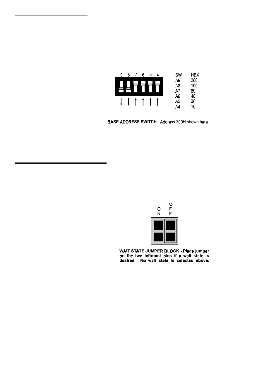
BASE ADDRESS
The InstaCal program will request that you 'SELECT BASE ADDRESS', which
allows you to choose a desired base address and adjusts the base address if necessary
to place it on an 16 bit boundary.
After a base address is chosen, a
diagram of the switch setting is
drawn on the PC screen. Set the
switches on your base address
switch as shown on the diagram.
Unless there is already a board in
your system which uses address
300 HEX (768 Decimal) then you
can leave the switches as they are
set at the factory.
In the example shown here, the CIO-DDA06 is set for base address 300H (768 Decimal).
WAIT STATE JUMPER
The CIO-DDA06 boards have a wait
state jumper which can enable an onboard wait state generator. A wait
state is an extra delay injected into the
processor's clock via the bus. This
delay slows down the processor when
the processor addresses the CIODDA06 board so that signals from
slow devices (chips) will be valid.
The wait state generator on the CIODDA06 is only active when the CIODDA06 is being accessed. Your PC
will not be slowed down in general by
using the wait state.
4
Page 7
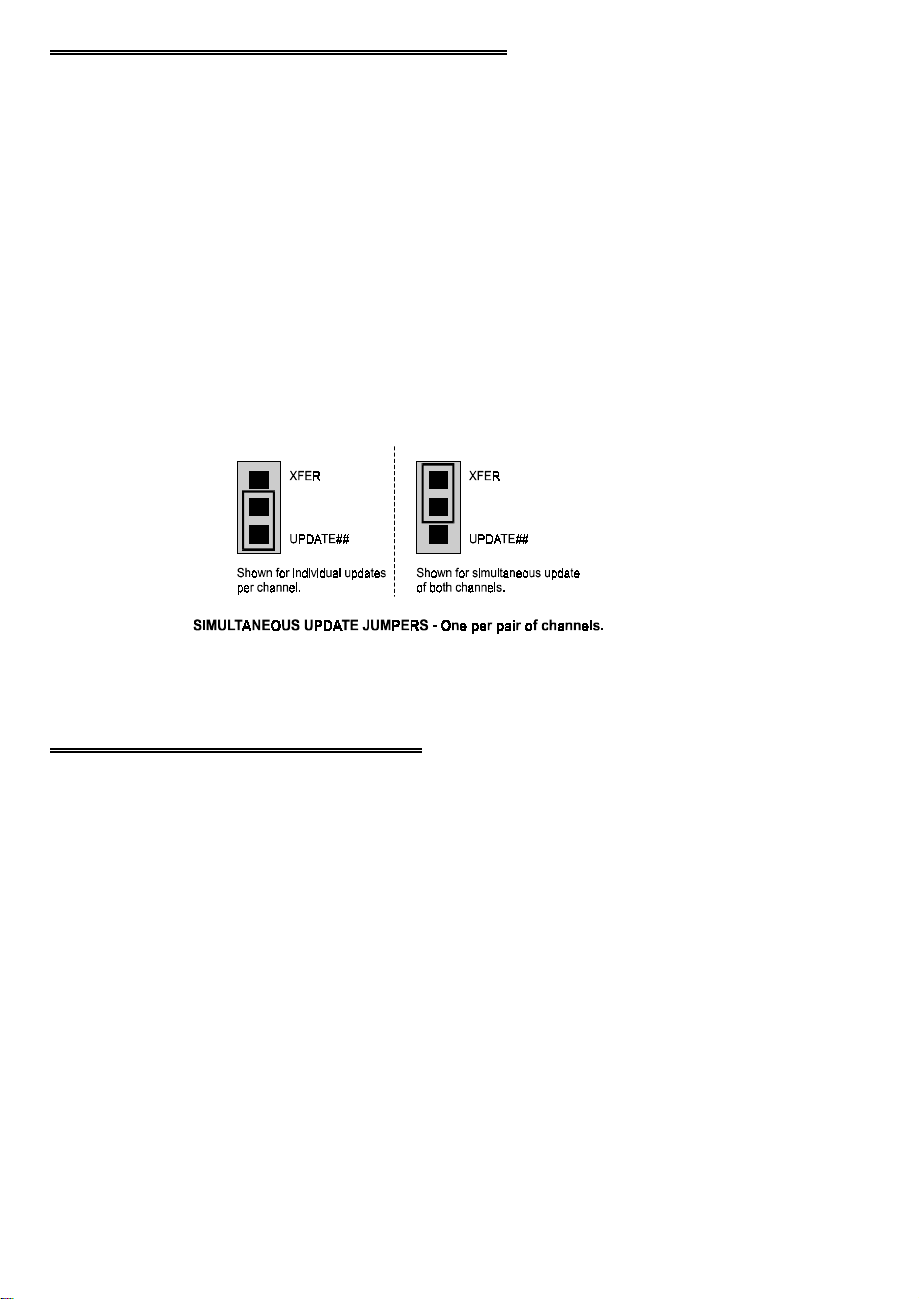
SIMULTANEOUS UPDATE JUMPER
The analog outputs may be jumpered so that new output data is held until several
DACs have been loaded with new digital data, then, as a group, have that new data
update the voltage outputs. The simultaneous update occurs whenever any of the
CIO-DDA06 addressed BASE+0 through BASE+Care read.
The analog output chips on the CIO-DDA06 are dual DACs. Two analog outputs are
on each chip. A single jumper sets both DACs on a single chip to be simultaneous
UPDATE or individual TRANSFER update.
The diagram below shows the jumper block in each configuration. If you look on the
CIO-DDA06 board, you will see the numbers 45, 23, and 01 ( left to right) next to the
simultaneous update jumpers. Those numbers indicate which channels that jumper
selects.
If you are familiar witht the DDA-06, you have probably noticed that only
pairs, and not individual channels, may be selected for simultaneous update.
POWER UP STATE JUMPER
The analog outputs may be jumpered so that their power up state is 0V. A single
jumper sets this option for all six channels. In the zero volts mode,“ZERO”, they are
held at 0V until one of the DAC “Most Significant Nibble” registers is written to and
then any of the DAC registers are read. In the standard mode,“STD”, they power up
in an undetermined state.
5
Page 8

The diagram below shows the jumper block in each configuration.
ANALOG OUTPUT RANGE SWITCH
The analog output voltage range of each channel may be set via a six position DIP
switch. The switches are located on the board directly below the calibra tion potentiometers and are labeled GAIN 5 through GAIN 0.
Set the switches for an individual channel as shown here.
RANGE
DNDNDNUPDNUP+/-10
DNDNUPDNDNUP+/-5
DNUPDNDNDNUP+/-2.5
UPDNDNDNDNUP+/-1.67
DNDNDNUPUPDN0-10
DNDNUPDNUPDN0-5
DNUPDNDNUPDN0-2.5
UPDNDNDNUPDN0-1.67
To set in a chosen range, read the switch positions as Up or DN (down) from left to
right in the row beside the range you desire.
For example, the ñ5V range is: UP DN DN UP DN DN.
If you are familiar with the DDA-06, you may have noticed that the CIODDA06 has more voltage ranges available but lack a 4-20mA output.
6
Page 9

INSTALLING THE CIO-DDA06 IN THE COMPUTER
Turn the power off.
Remove the cover of you computer. Please be careful not to dislodge any of the
cables installed on the boards in your computer as you slide the cover off.
Locate an empty expansion slot in your computer.
Push the board firmly down into the expansion bus connector. If it is not seated fully
it may fail to work and could short circuit the PC bus power onto a PC bus signal.
This could damage the motherboard in your PC as well as the CIO-DDA06.
CABLING TO THE CIO-DDA06
The CIO-DDA06 connector is accessible through the PC/AT expansion bracket. The
connector is a standard 37 pin male connector. A mating female connector may be
purchased from Radio Shack or other electronic supply outlets.
Those familiar with the DDA-06 will find the signal levels and pin assignments are identical with those on the CIO-DDA06. Those familiar with the
PIO12 and CIO-DIO24, 24H and 48 will find the pin assignments of the 24 digital bits
of those boards are identical with those on the CIO-DDA06
Several cabling and screw termination options are available.
DFCON-37
C37FFS-#
CIO-TERMINAL
ISO-RACK08
D connector, D shell and termination pins to contruct your
own cable.
2 foot (and longer) ribbon cable with 37 pin D connectors.C37FF-#
5 foot and 10 foot shielded round cable with molded ends
housing 37 pin connecotrs.
Simple, 40 position 4”x4” screw terminal board.CIO-MINI37
Full featured 4”x16” screw terminal board with prototyping
and interface circuitry.
24 position Solid State Relay mounting and interface board.SSR-RACK24
8 position Isolated Analog Module mounting and interface
board.
Enclosure for the MINI37.ENC-MINI37
Enclosure for larger external accessory boards.ENC-17-3
7
Page 10

SIGNAL CONNECTION
The analog outputs of the CIO-DDA06 are two-wire hook-ups. A signal, labeled D/A
# OUT on the connector diagram below, and a Low Level Ground (LLGND). The
low level ground is an ana log ground and is the ground reference which shoul d be
used for all analog hook-ups.
Possible analog output ranges are:
+/-1.67V+/-2.5V+/-5V+/-10VBipolar Ranges
and
0-1.67V0-2.5V0-5V0-10VUnipolar Ranges
See the range select switch in section 5.4
All the digital outputs inputs on the CIO-DDA06 connector are TTL level. TTL is an
electronics industry term, short for Transistor Transistor Logic, which describes a
standard for digital signals which are either at 0V or 5V. The binary logic inside the
PC is all TTL or LSTTL (Low power Schotky TTL).
Under normal operating conditions, the voltages on the 8255 pins range from 0 to
0.45 volts for the low state to between 2.4 to 5. 0 volts for the high state. At a voltage
of 0.45 volts the 8255 can safely sink 2 mA. At a voltage of 2.4 volts the 8255 can
source 0.4 mA. These values are typical of TTL devices.
The voltages and currents associated with external devices range from less than a hundred mA at a few volts for a small flash light bulb to 50 Amps at 220 volts for a large
electric range. Attempting to connect either of these devices directly to the CIODDA06 would destroy the I/O chip.
In addition to voltage and load matching, digital signal sources often need to be debounced. A complete discussion of digital interfacing will be found in the section on
Interface Electronics in this manual.
CONNECTOR DIAGRAM
The CIO-DDA06 connector and the is a 37 pin D type connector accessible from the
rear of the PC through the expansion backpla te. The signa ls availa ble are identical to
those of the DDA-06.
The connector accepts female 37 D type connectors, such as those on the C37FF-2, 2
foot cable with connectors.
8
Page 11

If frequent changes to signal connections or signal conditioning is required, please
refer to the information on the CIO-TERMINAL, CIO-SPADE50 and CIOMINITERM screw terminal boards.
9
Page 12

CALIBRATION
A calibration option is supplied with InstaCal.
The steps to calibrate the CIO-DDA06 are simple to follow. The are:
UNIPOLAR
1. To calibrate D/A 0, connect a DVM to analog output 0. The positive lead is
connected to D/A 0 OUT, Pin 18. The ground lead is connected to LLGND,
pin 19.
2. OFFSET ADJUST: Program the DAC with code=0. Adjust the offset
potentiometer for a reading of 0.000 volts.
3. GAIN ADJUST: Program the DAC with code = 4095. Adjust the potentiometer for the full scale (FS) voltage - 1 LSB. For example, if you have set
the D/A range switches for 0-10V, then (+FS - 1LSB) = (10 - 1LSB). One
LSB equals the full scale range divided by 4095. In this case, 10/4095 =
0.00244. So, (10 - 0.00244) = 9.998V
4. Repeat the process above for the other DACs, 1-5
BIPOLAR
1. To calibrate D/A 0, connect a DVM to analog output 0. The positive lead is
connected to D/A 0 OUT, Pin 18. The ground lead is connected to LLGND,
pin 19.
2. OFFSET ADJUST: Program the DAC with code = 2048. Adjust the offset
potentiometer for a reading of 0.000V on the DVM.
3. GAIN ADJUST: Program the DAC with code = 4095. Adjust the potentiometer for the positive full scale (+FS) voltage - 1 LSB. For example, if you
have set the D/A range switches for ñ5 V, then (+FS - 1LSB) = (5 - 1LSB).
One LSB equals the full scale range divided by 4095. In this case, 10/4095 =
0.00244. So, (5 - 0.00244) = 4.998V
4. Repeat the procedure for DACs 1-5.
10
Page 13

ARCHITECTURE
The CIO-DDA06 is a simple board to understand right down to its lowest level. All
control and data is read/written with simple I/O read and write signals. No interrupt
or DMA control software is required. Hence, the board's functions are easy to control
directly from BASIC, C or PASCAL.
Architecturally, the board may be viewed as two separate function blocks (see the
block diagram below). The digital block consists of a single 82C55, 24 line digital
I/O chip. The analog block consists of 3 identical circuits, each comprised of one dual
DAC, two OP07 output buffers and range control. Each of the analog outputs may be
individually controlled, or groups of 2, 4 or all 6 outputs may be controlled simultaneously.
CONTROL & DATA REGISTERS
The CIO-DDA06 has 12 analog output registers. There are two for each channel, one
for the lower 8 bits and one for the upper 4 bits. An additional 4 address are occupied
by the 82C55 data (3) and control (1) registers. The board occupies 16 I/O addresses
in all.
The first address, or BASE ADDRESS, is determined by setting a bank of switches on
the board.
A register is easy to read and write to. Most often, register manipulation is best left to
ASSEMBLY language p rograms as most of the CIO-DDA06 po ssible functions are
implemented in an easy to use BASIC CALL.
The register descriptions all follow the format:
01234567
A0A1A2A3A4A5A6A7
Where the numbers along the top row are the bit positions within the 8 bit byte and the
numbers and symbols in the bottom row are the functions associated with that bit.
To write to or read from a register in decimal or HEX, the following weights apply:
11
Page 14

HEX VALUEDECIMAL VALUEBIT POSITION
110
221
442
883
10164
20325
40646
801287
To write a control word or data to a register, the individual bits must be set to 0 or 1
then combined to form a Byte. Data read from registers must be analyzed to determine which bits are on or off.
The method of programming required to set/read bits from bytes is beyond the scope
of this manual. It will be covered in most Introduction To Programming books, available from a bookstore.
In summary form, the registers and their function are listed on the following table.
Within each register are 8 bits which may constitute a byte of data or 8 individual bit
set/read functions.
READ FUNCTIONWRITE FUNCTIONADDRESS
Initiate simultaneous up/enable DACsD/A 0 Least Significant ByteBASE + 0
Initiate simultaneous up/enable DACsD/A 0 Most Significant NibbleBASE + 1
Initiate simultaneous up/enable DACsD/A 1 Least Significant ByteBASE + 2
Initiate simultaneous up/enable DACsD/A 1 Most Significant NibbleBASE + 3
Initiate simultaneous up/enable DACsD/A 2 Least Significant ByteBASE + 4
Initiate simultaneous up/enable DACsD/A 2 Most Significant NibbleBASE + 5
Initiate simultaneous up/enable DACsD/A 3 Least Significant ByteBASE + 6
Initiate simultaneous up/enable DACsD/A 3 Most Significant NibbleBASE + 7
Initiate simultaneous up/enable DACsD/A 4 Least Significant ByteBASE + 8
Initiate simultaneous up/enable DACsD/A 4 Most Significant NibbleBASE + 9
Initiate simultaneous up/enable DACsD/A 5 Least Significant ByteBASE + 10
Initiate simultaneous up/enable DACsD/A 5 Most Significant NibbleBASE + 11
Initiate simultaneous up/enable DACsPort A Input of 8255BASE + 12
Initiate simultaneous up/enable DACsPort B InputBASE + 13
Initiate simultaneous up/enable DACsPort C InputBASE + 14
Initiate simultaneous up/enable DACsNoneBASE + 15
12
Page 15

ANALOG REGISTERS
BASE ADDRESS +0 through +11
WRITE
Writing to any DAC "most significant nibble" is the first step in enabling the outputs
when the "Zero" power up mode is set.
READ
Reading these registers is the second step in enabling the DAC outputs when the
"Zero" powerup mode is set as well as initialinzing a simultaneous update.
NOTE: Even if you are not using the simultaneous up date fea ture, you must perfor m
a read to enable the DAC outputs if you are using the "ZERO" power up mode
feature.
DIGITAL I/O REGISTERS
D/A 0 LEAST SIGNIFICANT 8 BITS
BASE ADDRESS + 0 300 HEX, 768 Decimal
01234567
D12D11D10D9D8D7D6D5
D/A 0 MOST SIGNIFICANT 4 BITS
BASE ADDRESS + 1 301 HEX, 769 Decimal
01234567
D4D3D2D1XXXX
Writing data to the LSB loads that data into the D/A load register b ut does not upd ate
the D/A output. Writing data to the MSB both loads the uppe r 4 bits of the 12 bit
digital value and updates the output of the D/A.
The function and bit layout of the remaining 10 registers (5 D/As) is identical to that
shown above.
PORT A DATA
BASE ADDRESS + 12 30C HEX, 780 Decimal
01234567
A0A1A2A3A4A5A6A7
Pin 37Pin 36Pin 35Pin 34Pin 33Pin 32Pin 31Pin 30
13
Page 16

PORT B DATA
BASE ADDRESS + 13 30D HEX, 781 Decimal
01234567
B0B1B2B3B4B5B6B7
Pin 10Pin 9Pin 8Pin 7Pin 6Pin 5Pin 4Pin 3
Ports A & B may be programmed as input or output. Each is written to and read from
in Bytes, although fo r control and monitor ing purposes the individua l bits are more
interesting. it set/reset and bit read functions require that unwanted bits be masked out
of reads and ORed into writes.
PORT C DATA
BASE ADDRESS + 14 30E HEX, 782 Decimal
01234567
C1C2C3C4C5C6C7C8
CL1CL2CL4CL4CH1CH2CH3CH4
128 Bit
Weight
80 Bit
Port C may be used as one 8 bit port of either input or output, or it may be split into
two 4 bit ports which may be independently input or output. The notation for the
upper 4 pit port is PCH3 - PCH0, and for the lower, PCL3 - PCL0.
40
Weight
HEX
12481632 Dec.64
12481020
Pin 29Pin 28Pin 27Pin 26Pin 25Pin 24Pin 23Pin 21
Although it may be split, every read and write to port C carries 8 bits of data so
unwanted information must be ANDed out of reads, and writes must be ORed with the
current status of the other port.
OUTPUT PORTS
In 8255 mode 0 configuration, ports configured for output hold the output data written
to them. This output byte may be read back by reading a port configured for output.
INPUT PORTS
In 8255 mode 0 configuration, ports configured for input read the state of the input
lines at the moment the read is executed, transitions are not latched. or information on
modes 1 (strobed I/O) and 2 (bi-directional strobed I/O), you will need to acquire an
Intel or AMD data book and see the 8255 data sheet.
8255 CONTROL REGISTER
BASE ADDRESS + 15 30F HEX, 783 Decimal
01234567
CLBM1CHAM2M3MS
Group BGroup A
14
Page 17

The 8255 may be programmed to operate in Input/ Output (mode 0), Strobed Input/
Output (mode 1) or Bi-Directional Bus (mode 2).
When the PC is powered up or RESET, the 8255 is reset. This places all 24 lines in
Input mode and no further programming is needed to use the 24 lines as TTL inputs.
To program the 8255 for other modes, the following control code byte must be assembled into on 8 bit byte.
MS = Mode Set. 1 = mode set active
M3 M2 Group A Function
0 0 Mode 0 Input / Output
0 1 Mode 1 Strobed Input / Output
1 X Mode 2 Bi-Directional Bus
A B CL CH Independent Function
1111Input
0000Output
M1 = 0 is mode 0 for group B. Input / Output
M1 = 1 is mode 1 for group B. Strobed Input / Output
The Ports A, B, C High and C Low may be independently programmed for input or
output. Te two groups of ports, group A and group B, may be independently programmed in one of several modes. The most commonly used mode is mode 0, input /
output mode. The codes for programming the 8255 in this mode are shown below.
D7 is always 1 and D6, D5 & D2 are always 0.
15
CLBCUADECHEXD0D1D3D4
OUTOUTOUTOUT128800000
INOUTOUTOUT129811000
OUTINOUTOUT130820100
ININOUTOUT131831100
OUTOUTINOUT136880010
INOUTINOUT137891010
OUTININOUT1388A0110
INININOUT1398B1110
OUTOUTOUTIN144900001
INOUTOUTIN145911001
OUTINOUTIN146920101
ININOUTIN147931101
OUTOUTININ152980011
INOUTININ153991011
OUTINININ1549A0111
ININININ1559B1111
Page 18

PC/XT/AT BUS INTERFACE
The CIO-DDA06 employs the PC bus for power, communications and data transfer.
As such it draws power from the PC, monitors the address lines and control signals
and responds to it's I/O address, and it receives and places data on the 8 data lines.
The BASE address is the most important user selectable bus related feature of the
CIO-DDA06. The base address is the location that software writes to and reads from
when communicating with the CIO-DDA06.
The base addr ess switch is the means for setting the base addre ss. Each switch position corresponds to one of the PC bus address lines. By placing the switch down, the
CIO-DDA06 address decode logic is instructed to respond to that address bit.
A complete address is constructed by calculating the HEX or decimal number which
corresponds to all the address b its the CIO-DDA06 has been instructed to resp ond to.
For example, shown to the right are address 9 and 8 down, all others up.
Address 9 = 200H (512D) and address 8 = 100H (256D), when added together they
equal 300H (768D).
Certain address are used by the PC, others are free and may be used by the CIODDA06 and other expansion boards. We recommend BASE = 300H (768D) be tried
first.
The CIO-DDA06 BASE switch may
be set for address in the range of 0003F0 so it should not be hard to find a
free address area for you CIO-DDA06.
Once again, if you are not using IBM
prototyping cards or some other board
which occupies these addresses, then
300-31F HEX are free to use.
Address not specifically listed, such as
390-39F, are free.
FUNCTIONHEX
RANGE
FUNCTIONHEX
RANGE
EGA2C0-2CF8237 DMA #1000-00F
EGA2D0-2DF8259 PIC #1020-021
GPIB (AT)2E0-2E78253 TIMER040-043
SERIAL PORT2E8-2EF8255 PPI (XT)060-063
SERIAL PORT2F8-2FF8742 CONTROLLER (AT)060-064
16
Page 19

070-071
CMOS RAM & NMI MASK (AT)
PROTOTYPE CARD300-30F
PROTOTTYPE CARD310-31FDMA PAGE REGISTERS080-08F
HARD DISK (XT)320-32F8259 PIC #2 (AT)0A0-0A1
PARALLEL PRINTER378-37FNMI MASK (XT)0A0-0AF
SDLC380-38F8237 #2 (AT)0C0-0DF
SDLC3A0-3AF80287 NUMERIC CO-P (AT)0F0-0FF
MDA3B0-3BBHARD DISK (AT)1F0-1FF
PARALLEL PRINTER3BC-3BFGAME CONTROL200-20F
EGA3C0-3CFEXPANSION UNIT (XT)210-21F
CGA3D0-3DFBUS MOUSE238-23B
SERIAL PORT3E8-3EFALT BUS MOUSE23C-23F
FLOPPY DISK3F0-3F7PARALLEL PRINTER270-27F
SERIAL PORT3F8-3FFEGA2B0-2BF
OPTIONAL DC/DC CONVERTER
An optional DC/DC converter may be installed . The DC/DC
converter provides +/-15V, eliminating the need for the +/-12V supply of the PC.
This option is useful only to those who wish to install the CIO-DDA06 in a PC that
does not have both 12V, such as a portable.
This $30 option must be specified at the time of order by adding a CIO-PG408 to the
order.
17
Page 20

POWER CONSUMPTION
CIO-DDA06
+5V Supply 435 mA typical / 525 mA max.
+12V Supply 50mA typical / 80 mA max.
-12V Supply 120 mA typical / 160 mA max
CIO-DDA06 WITH DC/DC INSTALLED
+5V Supply 935 mA typical / 1.025A max.
ANALOG OUTPUTS
Channels 6
Resolution 12 bits (1 part in 4095)
D/A type Dual DAC, AD7237
Latches Double buffered w/ optional sim. update.
Linearity 1/2 bit
Monotonicity 1/2 bit
Temperature drift 1 ppM typical, 3 ppM max @ 0
15 ppM typical, 30 ppM max @ full scale gain.
Output ranges 0 to 10 volts
0 to 5 volts
0 to 2.5 volts
0 to 1.67 volts
10 volts
5 volts
2.5 volts
1.67 volts
Load current 5mA max
Short circuit current 40mA max
Output resistance <0.1 ohm
Settling time +FS 0.01% 3uS typical, 5uS max
Settling time -FS 0.01% 5uS typical, 10uS max
Power Up Mode 0V(with jumper set to "Zero")
undefined jumper set to "STD")
SPECIFICATIONS
18
Page 21

DIGITAL I/O
TTL LEVEL DIRECT TO/FROM 8255 CHIPS
8255 output high 2.4 V min @ -200 uA
8255 output low 0.5 V max @ 2.5 mA
8255 input high 2.0 V min, 7 V max
8255 input low -0.5 V min, 0.8 V max
8255 drive capability 5 LSTTL loads
ENVIRONMENTAL
Operating Temperature 0 - 50 deg C
Storage Temperature -20 to 70 deg C
Humidity 0 to 90% non-condensing
Weight 6.35 oz
19
Page 22

EC Declaration of Conformity
Analog Output BoardCIO-DDA06
DescriptionPart Number
to which this declaration relates, meets the essential requirements, is in conformity
with, and CE marking has been applied according to the relevant EC Directives listed
below using the relevant section of the following EC standards and other normative
documents:
EU EMC Directive 89/336/EEC
compatibility.
EU 55022 Class B
characteristics of information technology equipment.
EN 50082-1
IEC 801-2
and control equipment.
IEC 801-3
measurements and control equipment.
IEC 801-4
equipment.
Carl Haapaoja, Director of Quality Assurance
: Electrostatic discharge requirements for industrial process measurement
: Radiated electromagnetic field requirements for industrial process
: Electrically fast transients for industrial process measurement and control
: Limits and methods of measurements of radio interference
: EC generic immunity requirements.
: Essential requirements relating to electromagnetic
Page 23

 Loading...