

Page 1

User's Guide
http://www.omega.com
e-mail: info@omega.com
CIO-DAS-TC
PCI-DAS-TC
Page 2

Table of Contents
1.0 INTRODUCTION
............................................
2.0 INSTALLATION
................................................
2.1 SOFTWARE INSTALLATION
....................................
2.1.1 WINDOWS 95, 98, NT AND ABOVE
.............................
2.1.2 UNIVERSAL LIBRARY INSTALLATION OPTIONS
2.1.3 FILE DEFAULT LOCATION
..................................
2.1.4 INSTALLATION QUESTIONS
...............................
2.1.5 INSTALLATION COMPLETION
..............................
2.1.6 DOS AND WINDOWS 3.x
....................................
2.2 CIO-DAS-TC HARDWARE INSTALLATION
......................
2.2.1 SETTING THE BASE ADDRESS SWITCH
........................
2.2.2 RUN InstaCAL
.............................................
2.2.3 PLUG IN THE CIO-DAS-TC BOARD
............................
2.2.4 RUN InstaCAL AGAIN
.......................................
2.3 PCI-DAS-TC HARDWARE INSTALLATION
.......................
2.3.1 PHYSICAL INSTALLATION
..................................
2.3.2 RUN InstaCAL
.............................................
2.3.3 TESTING THE INSTALLATION
...............................
2.4 EXTERNAL CONNECTIONS & THE CIO-STA-TC
2.4.1 DAS-TC CONNECTOR PINOUT
...............................
2.4.2 THE CIO-STA-TC
.........................................
2.4.3 OPEN THERMOCOUPLE DETECTION
........................
3.0 PROGRAMMING & APPLICATIONS
..........................
3.1 PROGRAMMING LANGUAGES
................................
3.2 PACKAGED THIRD-PARTY APPLICATIONS PROGRAMS
................
.................
........
Page 4
Page 6
Page 6
Page 6
Page 6
Page 6
Page 6
Page 6
Page 6
Page 7
Page 7
Page 7
Page 8
Page 8
Page 8
Page 8
Page 8
Page 9
Page 9
Page 9
Page 10
Page 10
Page 11
Page 11
Page 11
Page 3

Table of Contents
4.0 THEORY OF OPERATION
.....................................
4.1 ISOLATED ANALOG INPUT
....................................
4.2 PROCESSING AND CONTROL
.................................
4.3 PROCESS FLOW
..............................................
5.0 SELF-CALIBRATION
.......................................
6.0 REGISTER DESCRIPTION
..................................
6.1 PCI-DAS-TC REGISTER OVERVIEW
6.1.1 PCI Local Register Map
.....................................
6.1.2 Board I/O Register Map
.....................................
6.2 CIO-DAS-TC REGISTER OVERVIEW
6.3 REGISTER MAP DETAILS
.....................................
6.2 DUAL PORT RAM MEMORY MAP
6.3 DUAL PORT RAM BIT DEFINITIONS
6.3.1 Configuration Region (0x300 - 0x31F)
6.3.2 Float Region (0x320 - 0x363)
.................................
6.3.3 A/D Count Region (0x370 - 0x395)
6.3.4 AM188 Mailbox (0x3FE)
.....................................
6.3.5 PC Mailbox (0x3FF)
........................................
6.4 COMMANDS FROM THE PC TO THE DAS-TC
6.4.1 Modify sampling parameters
..................................
6.4.2 Modify one or more channel parameters
6.4.3 Read a single channel’s temperature
6.4.4 Read multiple channels’ temperature
6.4.5 Read A/D counts for all channels
6.4.6 Read the firmware version number
6.4.7 Read the voltages from all channels
............................
............................
..............................
...........................
..........................
.............................
....................
.........................
...........................
...........................
..............................
.............................
............................
Page 12
Page 12
Page 12
Page 12
Page 13
Page 14
Page 14
Page 14
Page 14
Page 15
Page 15
Page 16
Page 17
Page 17
Page 18
Page 18
Page 18
Page 18
Page 19
Page 19
Page 19
Page 19
Page 20
Page 20
Page 21
Page 21
Page 4

Table of Contents
6.5 ERROR CODES FROM THE DAS-TC
............................
6.6 HOW TO READ FLOATING POINT TEMPERATURE
7.0 ELECTRICAL SPECIFICATIONS
..........................
..............
Page 22
Page 22
Page 23
Page 5
1.0 INTRODUCTION
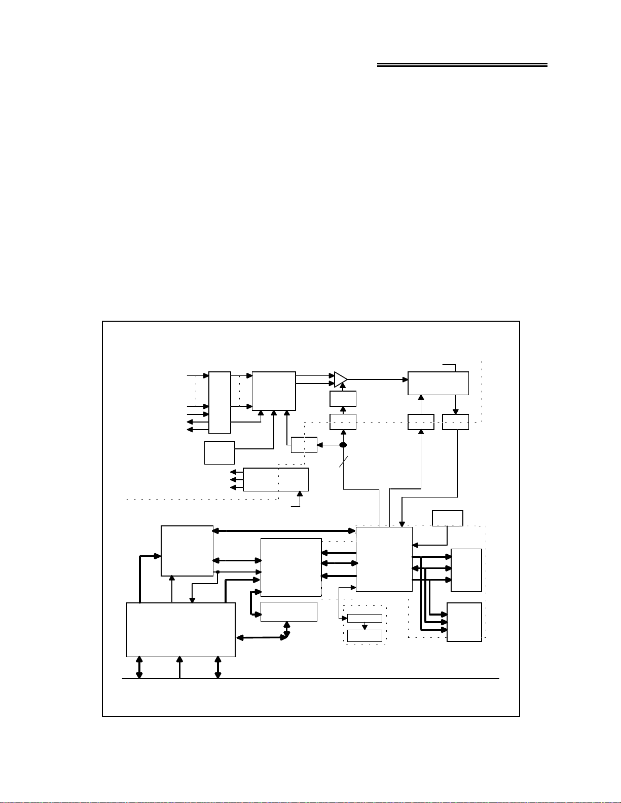
Thank you for purchasing a CIO-DAS-TC or PCI-DAS-TC. These boards represent the latest
technology and are easy to use, powerful and extremely accurate. The DAS-TC includes the CIO-STA-TC, a screw
terminal board with an isothermal block and CJC sensor, as well as a C37FFS-5 five-foot shielded cable.
The CIO-DAS-TC and PCI-DAS-TC are 16-channel thermocouple/voltage input boards for the ISA and PCI bus,
respectively. The DAS-TC boards accept seven different types of thermocouple input (J, K, E, T, R, S, and B), and
provide the user with a temperature in either degrees C or F. An onboard microprocessor handles all the control and
math functions including; CJC (Cold Junction Compensation), automatic gain and offset calibration, and thermocouple linearizati on, thus off-loading the computer CPU from performing these functions. The analog input section is
fully isolated from the computer. A block diagram of the DAS-TC is shown on the following page.
The CIO-DAS-TC and PCI-DAS-TC are similar in all respects except two: first, the CIO-DAS-TC is designed to
work with the ISA bus and the PCI-DAS-TC with the PCI bus. Second, the CIO-DAS-TC has an onboard dip switch
for setting the base address; while the PCI-DAS-TC is completely plug-and-play, with no jumpers or switches to set!
For the sake of clarity in this manual, we will refer to both boards collectively as DAS-TC, except where these two
differences apply.
The DAS-TC is supported by the powerful Universal Library driver package. The boards are also
supported by many third-party, high-level data acquisition software.
Isolated Analog Input Section
TC Input
Channels
0 - 15
CJC
+15ISO
(for
CJC)
Control
Signals
AGND
ISOLATION
BARRIER
PROGRAMMABLE
LOGIC
Board
Select
Control
Logic
Control
Registers
Input
Connector
37
pin
+10V
Prec.
Ref
RefRefRef
+5ISO
+15ISO
-15ISO
Local
Control
Address
+9.9V
PLX9052
PCI I/F
Control
Address
Data
20
Channel
Mux
DC/DC
Converter
+5System
DUAL PORT
SRAM
Data Bus
Transceiver
Data
INA
Gain
Mux
OPTO OPTO OPTO
OPTO
Address
Data
Control
D0:7
Processing and Control Section
CJC
Gain
7
Channel
Calibration
DEBUG
'232XCVR
10 PIN
Header
Select
AM188
CPU
Ser0
LOCAL BUS
+10VRef
V/F
Converter
CLK
IN
Control
Data
Address
Fout
OSC
SRAM
Flash/
Eprom
32Bit, 33MHz, 5V PCI BUS
PCI-DAS-TC Block Diagram
Page 4
Page 6
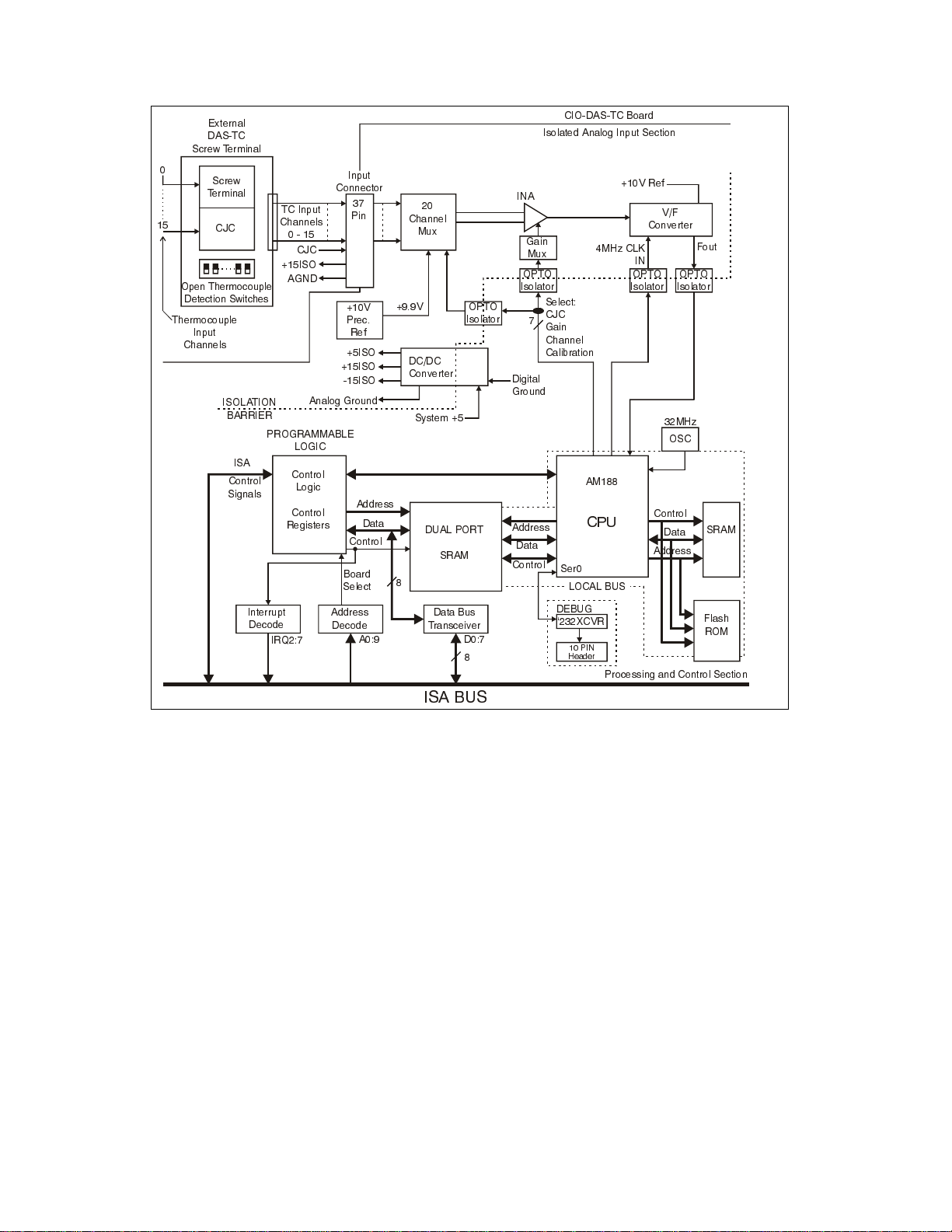
([WHUQDO
'$67&
6FUHZ 7HUPLQDO
7HUPLQDO
2SHQ 7KHUPRFRXSOH
'HWHFWLRQ 6ZLWFKHV
7KHUPRFRXSOH
,QSXW
&KDQQHOV
6FUHZ
&-&
,62/$7,21
%$55,(5
,6$
&RQWURO
6LJQDOV
7& ,QSXW
&KDQQHOV
&-&
,62
$*1'
352*5$00$%/(
/2*,&
&RQWURO
/RJLF
&RQWURO
5HJLVWHUV
,QWHUUXSW
'HFRGH
,54
,QSXW
&RQQHFWRU
3LQ
9
3UHF
5HI
,62
,62
,62
$QDORJ *URXQG
$GGUHVV
'DWD
&RQWURO
%RDUG
6HOHFW
$GGUHVV
'HFRGH
$ '
&KDQQHO
0X[
9
'&'&
&RQYHUWHU
6\VWHP
2372
,VRODWRU
'8$/ 3257
65$0
'DWD %XV
7UDQVFHLYHU
,6$ %86
&,2'$67& %RDUG
,VRODWHG $QDORJ ,QSXW 6HFWLRQ
,1$
*DLQ
0X[
2372
,VRODWRU
'LJLWDO
*URXQG
$GGUHVV
'DWD
&RQWURO
6HOHFW
&-&
*DLQ
&KDQQHO
&DOLEUDWLRQ
$0
&38
6HU
/2&$/ %86
'(%8*
¶;&95
3,1
+HDGHU
0+] &/.
9 5HI
9)
&RQYHUWHU
,VRODWRU
0+]
26&
&RQWURO
'DWD
$GGUHVV
)RXW
2372
65$0
)ODVK
520
,1
2372
,VRODWRU
3URFHVVLQJ DQG &RQWURO 6 HFWLRQ
CIO-DAS-TC Block Diagram
Page 5
Page 7

2.0 INSTALLATION
The installation routine varies only slightly depending upon whether you are installing the CIO-DAS-TC or the
TM
PCI-DAS-TC board. The CIO-DAS-TC r equire s that you run the included Insta
program, then verifying and,
Cal
if necessary, changing t he base addr ess using an onboar d dip switc h before pl ugging the board in. If you ar e install ing the PCI-DAS-TC, you need only plug it in. The base address is allocated by the PCI plug & play procedure.
2.1 SOFTWARE INSTALLATION
2.1.1 WINDOWS 95, 98, NT AND ABOVE
If you will be using the Universal Library with your board, insert the Universal Library diskette or CD in an appropriate drive run the program SETUP.EXE, and follow the installation instructions provided. This program will install
both Insta
98, you will have the option of installing the 16-bit and/or 32-bit library. Unless you have a specific reason to use the
16-bit library (e.g. compatibility with an existing program) install the 32-bit version. Please note that the DAS-TC
boards are not currently supported by the 16-bit library and so are not currently compatible with the DOS or
Windows 3.x operating systems. Please contact the factory if you require 16-bit library support.
If you are not using the Universal Library, insert the disk or CD labeled Insta
run SETUP.EXE. The install wizard will now launch and you will then be prompted for additional information.
Follow the instructions and, if possible, accept the defaults, especially if this is your first installation. It will be easier
for us to assist you in the unlikely event of trouble during your system setup and operation.
2.1.2 UNIVERSAL LIBRARY INSTALLATION OPTIONS
The Universal Library p rovides example programs for a wide variety of programmi ng la nguages. If you are installing
the Universal Library, an "Installation Options" dialog box will allow you to select which languages' example
programs are loaded onto your computer. Select the desired example programs by checking the appropriate box(s).
TM
( setup and test utility) and the Universal Library. (If you are using Windows 95 or
Cal
TM
Cal
into an appropriate drive, and
2.1.3 FILE DEFAULT LOCATION
InstaCal will place all appropriate files in "C:CB" If you change this default location remember where the installed
files are placed as you may need to access them later.
2.1.4 INSTALLATION QUESTIONS
At the end of the installation process the installation wizard will ask a series of questions updating your startup files.
Unless you have knowledge to the contrary, simply accept the default (YES) when prompted. You will also be asked
if you would like to read an updated README file. If possible, please choose yes and take a look at the information
in the file. It will include the latest information regarding the software you are installing.
2.1.5 INSTALLATION COMPLETION
After the installation of InstaCal is complete you should restart your computer to take advantage of changes made to
the system.
2.1.6 DOS AND WINDOWS 3.x
Most users are now installing PCI Bus boards in systems with 32-bit operating syste ms (e.g., Windows 95, 98 or
NT). The DAS-TC is not currently supported by the 16-bit library required to run under DOS or Windows 3.x.
Please contact us if your application is running under DOS or Windows 3.x.
Page 6
Page 8
2.2 CIO-DAS-TC HARDWARE INSTALLATION
2.2.1 SETTING THE BASE ADDRESS SWITCH
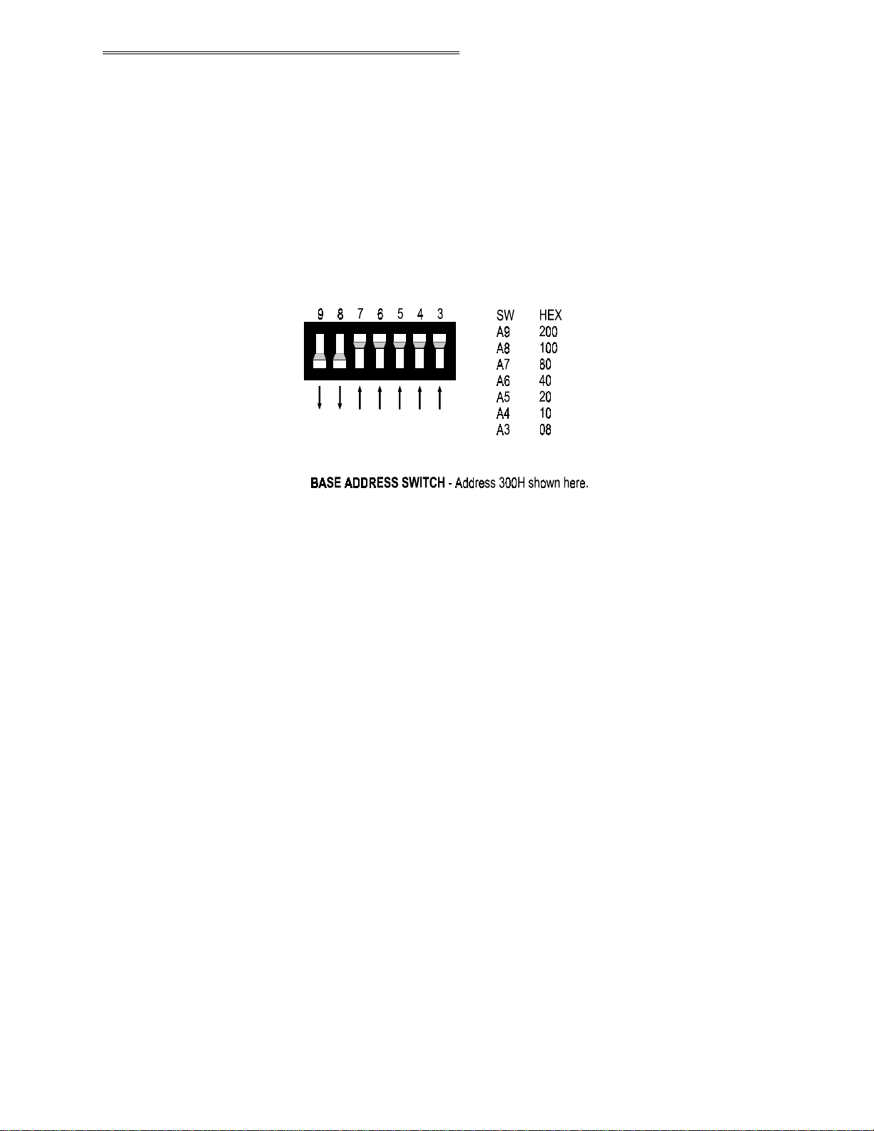
Prior to installing the CIO-DAS-TC board, you need to set the base address by using the dip switch located on the
board. The easiest way to set the base address switch is to let InstaCAL show you the correct settings. This process is
described in the section (2.2.2).
However, if are already familiar with setting ISA base addresses, you may use the base address switch description
below to guide your base address selection.
Unless there is already another board in your system using address 300 HEX (768 Decimal), you can leave the
switches as they are set at the factory. The example shown in the following diagram shows the settings for the factory
default base address of 300H.
A complete address is constructed by calculating the HEX or decimal number which corresponds to all the address
bits the CIO-DAS-TC has been instructed to respond to. In the default configuration, shown above, addresses 9 and
8 are DOWN, and all others are UP. Address 9 = 200H (512D) and address 8 = 100H (256D), when added together
they equal 300H (768D).
NOTE
DO NOT PAY ATTENTION TO THE NUMBERS PRINTED ON THE SWITCH. PLEASE REFER
TO THE NUMBERS PRINTED IN WHITE ON THE PRINTED CIRCUIT BOARD!
The InstaCAL software package will also help you set the base address switch. If you have questions regarding the
following diagram, run InstaCAL, and follow the instructions provided.
2.2.2 RUN InstaCAL
InstaCal
To run
TM
from Windows 95, 98 or NT use the familiar START>PROGRAM>ComputerBoards>InstaCAL.
Alternatively you may use the START>RUN sequence, type INSCAL32 and hit OK, or find the file named
INSCAL32.EXE using your file management system (located in C:\CB\ unless you selected an alternative directory
during installation) and double click your mouse on it.
1. Select
2. Select
Install
(either highlight it and hit enter or double click your mouse on it).
Add Board
3. Select the CIO-DAS-TC
4. Select
5. Select
Install
again
Configure
. The CIO-DAS-TC switch selection options will be displayed.
Page 7
Page 9

2.2.3 PLUG IN THE CIO-DAS-TC BOARD
Once you are done selecting and verifying the base address, you may shut the computer off and open the case.
Locate an empty ISA expansion slot in your computer. Push the board firmly down into the expansion bus
connector. If it is not seated fully it may fail to work and could short circuit the PC bus power onto a PC bus signal.
This could damage the motherboard in your PC as well as the DAS-TC. We also highly recommend that you use the
screw provided on your computer's back plate to secure the DAS-TC in it's location.
Replace the cover to the computer and turn it on. Plug one end of the cable provided into the DAS-TC board, and the
other into the CIO-STA-TC. Your hardware is now installed.
2.2.4 RUN InstaCAL AGAIN
Run the InstaCal progr am in order to test your bo ard and co nfigure it for run-time use. By confi guring the boar d,
you add information to the configuration file, cb.cfg, that is used by the Universal Library and other third-party data
acquisition packages that use the Universal Library to access the board.
Check that the CIO-DAS-TC is still listed as an installed board. Then proceed to the " Calibrate" or "T est" functions
of InstaCAL to assure that your board is functioning properly. Once the board has been tested, select FILE then
Exit, and the configuration file will be written to your hard disk.
2.3 PCI-DAS-TC HARDWARE INSTALLATION
2.3.1 PHYSICAL INSTALLATION
The PCI-DAS-TC is completely plug and play. Simply follow the steps shown below to install your PCI hardware.
1.
Turn your computer off, unplug it, open it up and insert the PCI board into any available PCI slot.
2.
Close your computer up, plug it back in and turn it on. Plug one end of the cable provided into the DAS-TC
board, and the other into the CIO-STA-TC. Your hardware is now installed. Run InstaCal
may use one of the built-in test functions to assure the board is operating properly
3.
Windows will automatically detect the board as it starts up. If the board's configuration file is already on the
system, it will load without user interaction. If the configuration file is not detected, you will be prompted to
insert the disk containing it. The required file is on the InstaCal or Universal Library disk you received with
your board. Simply insert the CD (or Disk 1 if your software is on floppy disk) into an appropriate drive and
click on CONTINUE. The appropriate file should then be automatically loaded and the PCI board will
appear in the Device Manager under DAS Component.
2.3.2 RUN InstaCAL
Run the InstaCal progr am in order to test your bo ard and co nfigure it for run-time use. By confi guring the boar d,
you add information to the configuration file, cb.cfg, that is used by the Universal Library and other third-party data
acquisition packages that use the Universal Library to access the board.
Launch InstaCal by going to your Start Menu then to Programs, then to ComputerBoards, and finally choosing Insta-
Cal. You may also launch the program by going to START >RUN and typing INSCAL32, or by finding the file
named "inscal32.exe" in your installation directory and double clicking it.
InstaCal will display a dialog box indicating the boards that have been detected in the system. If there are no other
boards currently installed by InstaCal, then the PCI-DAS-TC board will be assigned board number 0. Otherwise it
will be assigned the next available board number.
TM
again and you
You can now view and change the board configuration by clicking the properties icon or selecting the
Install>Configure menu.
Page 8
Page 10

In the PCI-DAS-TC installation, InstaCal reads the base address from the PCs BIOS and stores it in the configuration
file CB.CFG. This file is accessed by the Universal Library for programmers. Note also that the Universal Library is
the I/O board interface for packaged applications such as Labtech Notebook and HP-VEE, therefore the InstaCal
settings must be made in order for these and other third-party applications to run.
A word of warning is in order here. We do not advise direct writes to the addresses simply by reference to the base
address of the PCI board I/O registers. Since the addresses assigned by the PCI plug & play software are not under
your control, there is no way to guarantee that your program will run in any other computer. In addition, when you
install new systems or components in your computer, previous base address assignments may be changed, or a
particular board may be moved. It is best to use a library such as Universal Library or a program such as HP-VEE to
make measurements with your PCI board.
2.3.3 TESTING THE INSTALLATION
With InstaCal running,
a.
Select the board you just installed
b.
Select the "Test" function
c.
Follow the instructions provided to test for proper board operation.
2.4 EXTERNAL CONNECTIONS & THE CIO-STA-TC
2.4.1 DAS-TC CONNECTOR PINOUT
The DAS-TC uses a single 37-pin connector on the back plate of the board to bring out 16 thermocouple input
channels, CJC input, and ground. See the following connector diagram for the correct pinouts on the back plate of
the DAS-TC.
Both the CIO-DAS-TC and the PCI-DAS-TC come with the CIO-STA-TC, a screw terminal board that provides an
isothermal block and cold-junction sensor, as well as with the C37FFS-5, a 5 foot shielded cable. A descriptio n of
these items is contained in the following section
9 ,62/$7(' 92/7$*( 6285&(
&+ /2
&+ /2
$1$/2* *5281'
&+ /2
&+ +,
&+ /2
&+ +,
&+ /2
&+ +,
&+ /2
&+ +,
&+ /2
&+ +,
&+ /2
&+ +,
&K /2
&+ +,
$1$/2* *5281'
121(
&+ +,
+,
&+
&+ /2
&+ +,
&+ /2
&+ +,
&+ /2
&+ +,
&+ /2
&+ +,
&+ /2
&+ +,
&+ /2
&+ +,
&+ /2
&+ +,
&-& ,1387
Page 9
Page 11

2.4.2 THE CIO-STA-TC
The CIO-STA-TC is a specially configured screw terminal adapter board designed specifically for use with the
DAS-TC series. The board provides screw terminals for each thermocouple channel, a cold junction sensor
integrated into an isothermal bar, and the option of installing an "open thermocouple detection" circuit.
Each thermocoup le i nput is made thr ough two scr e w ter minals (o ne + and o ne -) . Simpl y connec t your ther moc oup le
wires to the appropriate terminals, connect the CIO-STA-TC to the DAS-TC with the shielded cable pro vided, and
your system is ready to go!
2.4.3 OPEN THERMOCOUPLE DETECTION
The only user configurable option in the CIO-STA-TC is the open thermocouple detection resistors. These are a
series of 20 MegOhm resistors that can be connected between the + terminal of the thermocouple, and a known input
voltage that is larger than any allowable thermocouple output.
The 20 MegOhm is large enough so that it does not affect the reading from the thermocouple, but if the thermocouple junction happ ens to open c ircuit, the 20 MegOhm will drive the inp ut voltage high enough, so the software can
recognize that it is not a valid thermocouple reading.
The open thermocouple detection circuitry is set via dip switch on the CIO-STA-TC. The DIP switches are labeled ,
and each channel has a unique switch. To enable the open thermocouple detection scheme, set the switch to on (up
towards the isothermal block). To disable the circuits, simply set the switch to off (down, towards the outside of the
board). The units are shipped with the open thermocouple detection circuitry disabled..
Page 10
Page 12

3.0 PROGRAMMING & APPLICATIONS
The DAS-TC is supported by the powerful Universal Library. We strongly recommend that you take
advantage of the Universal Library as your software interface. In particular, the complexity of the PCI-BIOS's
dynamic allocation of PCI bus addresses and internal resources makes the PCI-DAS-TC series very challenging to
program via direct register I/O operations.
3.1 PROGRAMMING LANGUAGES
The Universal Library provides complete access to the DAS-TC functions from a range of
Windows programming languages. If you are planning to write programs, or would like to run the example
programs for Visual Ba sic or a ny other l anguage, plea se re fer to the Uni versa l Libra ry manual . For de tails r egar ding
programming with Universal Library, please refer to the Universal Library documentation.
The optional VIX Components package may greatly simplify your programming effort. VIX Components is a set of
programming tools based on a DLL interface to Windows languages. A set of VBX, OCX, and ActiveX interfaces
allows point and click construction of graphical displays, analysis and control structures. Please see a
product catalog or contact us for a complete description of VIX Components.
3.2 PACKAGED THIRD-PARTY APPLICATIONS PROGRAMS
In addition to DAS-Wizard, many packaged third-party application programs such as Labtech
Notebook and HP-VEE have, or will soon have drivers for the DAS-TC. If the package you own does not appear to
have drivers for the DAS-TC, please fax or e-mail the package name and the revision number from the install disks.
We will research the package for you and advise how to obtain DAS-TC drivers.
Some application drivers that are included with Universal Library are not included with third-party application
packages. If you have purchased an application package directly from the software vendor, you may need to
purchase our Universal Library and drivers. Please contact us for more information on this topic.
Page 11
Page 13

4.0 THEORY OF OPERATION
4.1 ISOLATED ANALOG INPUT
The analog input section of the DAS-TC consists of a CJC (Cold Junction Compensation) sensor input, a 16 (differential) channel multiplexer, a precision 9.90V source, an analog ground source, a programmable gain amplifier
suitable for sc aling the seven thermocouple types, and a high frequency synchronous V-F A/D convert er. During
normal operation, the V-F converts the CJC input, calibrates the gain at a Gain = 1 using the 9.9 V input, o ffset using
the ground input, and measures the thermocouple or voltage depending on the setup. The CJC and the gain/offset
values are stored in onboard RAM to allow proper cold junction scaling and calibration. These parameters are
sampled continuously.
The V-F converter is the Analog Devices AD652 SVFC (Synchronous V-F Converter) which offers full scale
frequency up to 2 MHz and extremely low linearity error. The 4 MHz clock for the V/F converter is supplied by
TIMER1 and p asse s thro ugh o p to -iso lat io n. T he o utp ut o f the V /F c onve rt er , p assi ng bac k thro ugh o p to -iso lat io n, is
supplied to TIMER0. TIMER0 is gated on by TIMER2 for a period dependent upon the specified conversion
frequency of 50Hz, 60Hz or 400Hz. At the end of the sampling period, the count in TIMER0 represents the voltage
input. In general, the longer the count time, the higher the resolution and better the noise reduction, unless in the
case of periodic noise where the periodic frequency (i.e. 50, 60, and 400 Hz) is more effective in reducing the noise.
4.2 PROCESSING AND CONTROL
This section of the DAS-TC consists of ISA or PCI control and decode logic, a microcontroller and local memory to
perform channel scanning, CJC measurements, calibration, linearization, averaging, and voltage/temperature translation. The above parameters are set up from a configuration file which is downloaded by the PC to the microcontroller’s local memory through the d ua l po rt RAM. O nce the micro co ntr o lle r i s given the co mmand to star t c onve r sio ns,
these parameters are set on a channel-by-channel basis with data reported to the PC in the format specified by the
configuration file. For thermocouple inputs, the microcontroller reads the counter, adjusts the data based on the CJC
value and gain/offset calibration, then linearizes and converts the reading to the appropriate temperature units.
To perform linearization, the microcontroller gets the raw frequency count from TIMER0, translates that into bits,
factors in the CJC correction and gain/offset calibration, then refers to a previously stored lookup table stored in
ROM, with a separate table for each thermocouple. The lookup tables are a method to optimize the linearization by
using more reference points along areas of greatest temperature/voltage change instead of using mathematical translation, which requires lengthy polynomial manipulation. The lookup tables require finding two consecutive points,
one greater and the next less than the measured value, then interpolating the measured value to the temperature.
4.3 PROCESS FLOW
The PC itself performs very few functions for the DAS-TC. The driver software included with the DAS-TC board
will set up individual channels, including the thermocouple type, CJC on/off, voltage or thermocouple gain, channel,
and temperature units. The sample rate and sample averaging configuration are also set by the software driver,
though these settings are for all cha nnels. Both during initializ ation and when the configuratio n changes, this information will be passed to the CPU through the Dual Port RAM and stored for the specified channel. The PC will
notify the CPU to start taking measurements. When the CPU completes a conversion, an interrupt is generated so
that the PC reads the data from the dual port RAM which the CPU had written to. The 32-bit floating point data is
stored in four consecutive locations in the dual port RAM. See section 7.4 for more details on this process.
The onboard CPU has a much more complicated task. The CPU must set all the parameters for the channel selected
to convert. Once converted, it must get the data, adjust based on the CJC measurement stored, calibrate against
gain/offset error, linearize based on lookup tables for each associated thermocouple type, and report the data to the
PC through the dual p ort RAM. During this p roc ess, the CP U must go to the ne xt channel and set up the par ameters
for that channel to allow proper time for settling before the next conversion begins.
Page 12
Page 14

5.0 Self-Calibration
The DAS-TC is shipped fully-calibrated from the factory with calibration coefficients stored in nonvolatile RAM.
At run time, these calibration factors are loaded into system memory and are automatically retrieved each time a
different range is specified. The user has the option to recalibrate with respect to the factory-measured voltage
standards at any time by simply selecting the "Calibrate" option in InstaCal. InstaCAL will calibrate all channels at
all six ranges. Each channel takes less than a minute to calibrate.
Page 13
Page 15

6.0 Register Description
We strongly urge users to take advantage of the Universal Library software package rather than attempt to write
register level software for the DAS-TC series. The register level programming information is provided as a matter of
completeness only. Register level programming of this or any other PCI board is quite complex and should only be
attempted by a highly experienced programmer.
The PCI- and CIO-DAS-TC register maps are virtually identical. The PCI board actually provides two base
addresses. The first (BADR1) provides access to the board's PLX 9052 PCI interface chip. This address also
provides the interrupt control status and control registers for the board. The second address (BADR2) actually
performs the data and address reads and writes.
The CIO-DAS-TC only provides a single base address that is virtually identical to the BADR2 address on the PCI
board. The following sections provide a more detailed description of the various addresses and their functions.
6.1 PCI-DAS-TC REGISTER OVERVIEW
OPERATIONSWRITE FUNCTIONREAD FUNCTIONREGISTER
32-bitDWORDInterrupt ControlInterrupt StatusBADR1+4C hex
8-bit BYTEDual Port RAM Addr (LSBs)N/ABADR2 + 0
8-bit BYTEDual Port RAM Addr (MSBs)N/ABADR2 + 1
8-bit BYTEDual Port RAM Data WriteDual Port RAM Data ReadBADR2 + 2
8-bit BYTEN/AN/ABADR2 + 3
8-bit BYTEResets DAS-TC microprocessorResets DAS-TC microprocessorBADR2 + 4
8-bit BYTEDAS-TC Mode RegisterN/ABADR2 + 5
6.1.1 PCI Local Register Map
%$'5 &KH[
: PLX9052 Interrupt Register: Read/Write
01234567
INTEINTPOLINT---PCI_EN-
This register, as with all the 9052 registers, is 32-bits in length. Since the rest of the register has specific control
functions, they would need to be masked off in order to access the interrupt control functions.
INTE is the Local Interrupt Enable: 0 = disabled, 1 = enabled (default).
INTPOL is the Interrupt Polarity: 0 = active low (default), 1 = active high.
INT is the Interrupt Status: 0 = interrupt is not active, 1 = interrupt is active.
PCI_EN is the PCI Interrupt Enable: 0 = disabled (default), 1 = enabled. This control signal allows the interrupt to
be passed to the PCI bus.
The PC de-asserts the interrupt by reading the mailbox location 0x3FF
1
in the Dual Port RAM.
6.1.2 Board I/O Register Map
The PCI-DAS-TC and CIO-DAS-TC have virtually identical I/O register maps. These are described in section 6.3,
with any differences between the boards noted there.
1
Location 0x3FF is the mailbox for the right side of the DPRAM which is connected to the ISA bus. Please refer to the data
sheets for the Cypress CY7C130 and Cypress application note “Understanding Asynchronous Dual-Port RAMs”.
Page 14
Page 16

6.2 CIO-DAS-TC REGISTER OVERVIEW
OPERATIONSWRITE FUNCTIONREAD FUNCTIONREGISTER
8-bit BYTEDual Port RAM Addr (LSBs)N/ABADR + 0
8-bit BYTEDual Port RAM Addr (MSBs)N/ABADR + 1
8-bit BYTEDual Port RAM Data WriteDual Port RAM Data ReadBADR + 2
8-bit BYTEInterrupt Control RegisterInterrupt Status RegisterBADR + 3
8-bit BYTEResets DAS-TC microprocessorResets DAS-TC microprocessorBADR + 4
8-bit BYTEDAS-TC Mode RegisterN/ABADR + 5
A detailed description of the registers and their functions is provided in the following section (6.3).
6.3 REGISTER MAP DETAILS
%DVH
: Dual Port RAM Address Byte (LSB): Write Only
01234567
DPRA0DPRA1DPRA2DPRA3DPRA4DPRA5DPRA6DPRA7
%DVH
: Dual Port RAM Address Byte (MSB): Write Only
01234567
DPRA8DPRA9------
Select the location of the DPRAM to be accessed by writing its address to BASE+0 and BASE+1. The data from this
location can be read by reading from BASE+2 or data can be written to this location by writing to BASE+2
%DVH
: Dual Port RAM Data Byte: Read/Write
Data from the DPRAM can be read by reading this register. Conversely, data can be written to DPRAM by writing to
this location. The location of the DPRAM is specified in register BASE+0 and BASE+1 respectively.
01234567
DPRD0DPRD1DPRD2DPRD3DPRD4DPRD5DPRD6DPRD7
%DVH
: PC Interrupt Control Register: Write (No function on the PCI-DAS-TC)
Writing to this register selects the interrupt line used to interrupt the PC. The PC can determine the cause of the
2
interrupt and simultaneously de-assert the interrupt by reading mailbox location 0x3FF
in the DPRAM.
01234567
INT1INT2INT4-----
Interrupt Enable/Select:
Selected IRQINT1INT2INT4
None000
IRQ2010
IRQ3110
IRQ4001
IRQ5101
IRQ6011
IRQ7111
2
Location 0x3FF is the mailbox for the right side of the DPRAM which is connected to the ISA bus. Please refer to the data
sheets for the Cypress CY7C130 and Cypress application note “Understanding Asynchronous Dual-Port RAMs”.
Page 15
Page 17

%DVH
: PC Interrupt Status Register: Read (No function on the PCI-DAS-TC)
01234567
INT1INT2INT4---INTL/INTR/
INT1-INT4 : Interrupt that is selected by writing to BASE+3.
3
This bit is 0 when the microcontroller writes to the PC’s mailbox location 0x3FF in the DPRAM.
INTR/
The PC can determine the cause of the interrupt and/or status and simultaneously clear the INTR/ bit
(i.e. make it 1) by reading mailbox location 0x3FF in the DPRAM.
4
INTL/
This bit is 0 as soon as the PC writes to the microcontroller’s mailbox location 0x3FE in the
DPRAM. This bit will be 1 after the microcontroller has read its mailbox. The PC should only write
to the microcontroller’s mailbox when this bit is 1.
%DVH
Reading or writing to this register will reset the microcontroller on the DAS-TC
: DASTC reset register: Read/Write
5
.
01234567
--------
%DVH
: Mode select register : Write only
This register is used to select the mode of the DAS-TC on power-up. This register is read by the processor only
during power up initialization.
01234567
-------
MODE
MODE This bit is 0 for normal operation mode. In normal mode, the board executes the firmware. On
power up this bit is cleared.
If this bit is set to 1, the board is forced to download firmware via the dual port RAM and program
it into FLASH.
After toggling the MODE bit, the board should be reset, by writing to BASE+4 register, because
the processor reads the bit only during initialization.
6.2 DUAL PORT RAM MEMORY MAP
The PC and the AM188 processor in the DAS-TC board communicate and share data through a 1Kx8 d ual-port
RAM. The PC accesses the DPRAM indirectly via registers at address BASE+0 through BASE+2 as explained in
section on page . The AM188 processor, however, accesses the DPRAM directly.
The DPRAM is divided into regions where predefined data is written by one processor and read by the other. The
top most two bytes in the DPRAM have special hardware logic associated with them and serve as mailboxes. Byte
0x3ff is the PC’s mailbox and byte 0x3fe is the AM188’s
mailbox. When the PC writes to the AM188’s mailbox, it
is notified about the arrival of data by the assertion of the INTL/ signal. When the AM188 reads its mailbox this
signal is de-asserted. Conversely, when the AM188 writes to the PC’s mailbox, the PC is notified either via an inter-
rupt or by the INTR/ bit in register BASE+3. When the PC reads its mailbox, this signal is de-asserted.
3
This bit reflects the status of the INTR/ output of the DPRAM.
4
This bit reflects the status of the INTL/ output of the DPRAM.
5
Moving the reset control from BASE+3 to a separate register (BASE+4) insures that the DAS-TC is not accidentally reset.
Page 16
Page 18

Addr
(Hex)
300 - - AVG3 AVG2 AVG1 AVG0 RS1 RS0 Configuration to 188
310 - F1 F0 G1 G0 TCT2 TCT1 TCT0 CH0 Confi guration to 188
311 - F1 F0 G1 G0 TCT2 TCT1 TCT0 CH1 Confi guration to 188
31F - F1 F0 G1 G0 TCT2 TCT1 TCT0 CH15 Configuration to 188
320 D7 D6 D5 D4 D3 D2 D1 D0 CH0 Float (Byte 0) to PC
321 D7 D6 D5 D4 D3 D2 D1 D0 CH0 Float (Byte 1) to PC
322 D7 D6 D5 D4 D3 D2 D1 D0 CH0 Float (Byte 2) to PC
323 D7 D6 D5 D4 D3 D2 D1 D0 CH0 Float (Byte 3) to PC
324 D7 D6 D5 D4 D3 D2 D1 D0 CH1 Float (Byte 0) to PC
325 D7 D6 D5 D4 D3 D2 D1 D0 CH1 Float (Byte 1) to PC
326 D7 D6 D5 D4 D3 D2 D1 D0 CH1 Float (Byte 2) to PC
327 D7 D6 D5 D4 D3 D2 D1 D0 CH1 Float (Byte 3) to PC
35C D7 D6 D5 D4 D3 D2 D1 D0 CH15 Float (Byte 0) to PC
35D D7 D6 D5 D4 D3 D2 D1 D0 CH15 Float (Byte 1) to PC
35E D7 D6 D5 D4 D3 D2 D1 D0 CH15 Float (Byte 2) to PC
35F D7 D6 D5 D4 D3 D2 D1 D0 CH15 Float (Byte 3) to PC
360 D7 D6 D5 D4 D3 D2 D1 D0 CJC Float (Byte 0) to PC
361 D7 D6 D5 D4 D3 D2 D1 D0 CJC Float (Byte 1) to PC
362 D7 D6 D5 D4 D3 D2 D1 D0 CJC Float (Byte 2) to PC
363 D7 D6 D5 D4 D3 D2 D1 D0 CJC Float (Byte 3) to PC
D7 D6 D5 D4 D3 D2 D1 D0 Description of data Data
flow
* * * *
* * * *
** **
** **
** **
370 D7 D6 D5 D4 D3 D2 D1 D0 CH0 count (Byte 0) to PC
371 D7 D6 D5 D4 D3 D2 D1 D0 CH0 count (Byte 1) to PC
372 D7 D6 D5 D4 D3 D2 D1 D0 CH1 count (Byte 0) to PC
373 D7 D6 D5 D4 D3 D2 D1 D0 CH1 count (Byte 1) to PC
38E D7 D6 D5 D4 D3 D2 D1 D0 CH15 count (Byte 0) to PC
38F D7 D6 D5 D4 D3 D2 D1 D0 CH15 count (Byte 1) to PC
390 D7 D6 D5 D4 D3 D2 D1 D0 0V count (Byte 0) to PC
391 D7 D6 D5 D4 D3 D2 D1 D0 0V count (Byte 1) to PC
392 D7 D6 D5 D4 D3 D2 D1 D0 9.9V count (Byte 0) to PC
393 D7 D6 D5 D4 D3 D2 D1 D0 9.9V count (Byte 1) to PC
394 D7 D6 D5 D4 D3 D2 D1 D0 CJC count (Byte 0) to PC
395 D7 D6 D5 D4 D3 D2 D1 D0 CJC count (Byte 1) to PC
3FED7D6D5D4D3D2D1D0AM188 Mailbox to 188
3FFD7D6D5D4D3D2D1D0PC Mailbox to PC
6.3 DUAL PORT RAM BIT DEFINITIONS
6.3.1 Configuration Region (0x300 - 0x31F)
These 32 bytes in the DPRAM are used to set up and configure data acquisition parameters. The configuration
region specifies global parameters which affect all channels and parameters for each individual channel. Section on
page describes the sequence of operations required to set the configuration.
Page 17
Page 19

6DPSOLQJ 3DUDPHWHUV $GGUHVV [
RS1:0 Resolution:
Resolution (Hz)RS0RS1
50X0
6010
40011
AVG3-AVG0 The number of data values used in computing the moving average from each channel. The micro-
controller stores the values from each channel in a circular buffer whose size is specified by
AVG3-AVG0. When a new sample is acquired, it is added to the buffer overwriting the oldest
sample and the moving average is computed. This number must be between 0 and 15; the number
of samples used to compute the average is 1 more than this.
&KDQQHO 3DUDPHWHUV $GGUHVV [[I
This area sets the parameters for each individual channel:
F1:0 Temperature format.
F0F1
Centigrade00
Fahrenheit10
KelvinX1
G1:0 Voltage gain
TCT2:0 Thermocouple Type
Thermocouple TypeTCT0TCT1TCT2
B000
E100
J010
K110
R001
S101
T011
Not connected111
6.3.2 Float Region (0x320 - 0x363)
These bytes are used to store either the temperature or voltage from the channels. This region is divided into 4-byte
blocks where each block has the data from a channel.
6.3.3 A/D Count Region (0x370 - 0x395)
These bytes are used to store the average A/D count from the thermocouple channels, CJC channel and the ground
and 9.9V reference voltage on the board. This region is divided into 2-byte blocks where each block has the 16-bit
count from a channel.
6.3.4 AM188 Mailbox (0x3FE)
This byte is used to send commands to the microcontroller in the DAS-TC. Please refer to section for details about
the commands. When the PC writes to this location, bit INTL/ in BASE+3 becomes 0. After the microcontroller
reads from this location, INTL/ goes high.
6.3.5 PC Mailbox (0x3FF)
This byte is used by the DAS-TC to convey information to the PC. When the microcontroller in the DAS-TC writes
to this location, bit INTR/ in BASE+3 (see page ) becomes 0 and simultaneously the interrupt selected in BASE+3
is asserted. After the PC reads this location, INTR/ becomes 1 and the interrupt, if any is selected, is de-asserted.
Page 18
Page 20

6.4 COMMANDS FROM THE PC TO THE DAS-TC
This section describes the software commands between the PC and the DAS-TC. The commands carry out the
following operations.
•
Load a new configuration.
•
Read a single channel’s temperature.
•
Read multiple channels’ temperature.
•
Read the CJC temperature
•
Read version number of firmware.
6.4.1 Modify sampling parameters
a)
The PC modifies one or more of the sampling parameters in byte 0x300.
b)
The PC writes the following command to the AM188 mailbox in the DPRAM.
D0D1D2D3D4D5D6D7Addr
000000013FE
c)
The DAS-TC reads, processes the new configuration and then writes a return code into the PC mailbox in
DPRAM. This causes bit INTR/ in BASE+3 to go low and an interrupt (if any is selected) is asserted to the PC.
The PC can either poll INTR/ or respond to the interrupt. Note, that it may take some time for the DAS-TC to
set the new sampling parameters and start sampling.
d)
When bit INTR/ in BASE+3 is low, the PC reads the following return code from the PC mailbox. Reading the
mailbox causes INTR/ to go high and the selected interrupt to be de-asserted.
D0D1D2D3D4D5D6D7Addr
ERR0ERR1ERR2ERR3ERR40013FF
Please refer to the return codes given in the next section.
6.4.2 Modify one or more channel parameters
e)
The PC modifies one or more of the channel configuration bits in the configuration region of DPRAM (refer to
section ).
f)
The PC writes the following command to the AM188 mailbox in the DPRAM.
D0D1D2D3D4D5D6D7Addr
100000013FE
g)
The DAS-TC reads, processes the new configuration and then writes a return code into the PC mailbox in
DPRAM. This causes bit INTR/ in BASE+3 to go low and an interrupt (if any is selected) is asserted to the PC.
The PC can either poll INTR/ or respond to the interrupt.
h)
When bit INTR/ in BASE+3 is low, the PC reads the following return code from the PC mailbox. Reading the
mailbox causes INTR/ to go high and the selected interrupt to be de-asserted.
D0D1D2D3D4D5D6D7Addr
ERR0ERR1ERR2ERR3ERR40013FF
Please refer to the return codes given in the next section.
6.4.3 Read a single channel’s temperature
i)
The PC writes the following command to the AM188 mailbox in the DPRAM specifying the channel to be read
D0D1D2D3D4D5D6D7Addr
CHL0CHL1CHL2CHL310013FE
where CHL3-CHL0 specify the channel number.
b)
The DAS-TC writes the temperature into the specified channel’s 4-byte block and a return code into the PC
mailbox signifying that data is available in DPRAM. This causes bit INTR/ in BASE+3 to go low and an
Page 19
Page 21

interrupt (if any is selected) is asserted to the PC. The PC can either poll INTR/ or r e spond to the interrupt. Note
that the CJC channel’s temperature in Centigrade is simultaneously updated to bytes 0x360-0x363.
c)
When bit INTR/ in BASE+3 is low, the PC reads the following return code from the PC mailbox. Reading the
mailbox causes INTR/ to go high and the selected interrupt to be de-asserted.
D0D1D2D3D4D5D6D7Addr
ERR0ERR1ERR2ERR3ERR40013FF
Please refer to the return codes given in the next section.
d)
If there are no errors, the PC reads four bytes of data for the selected channel from the float region of the
DPRAM. Please refer to section on page for details about data organization in the dual port RAM.
6.4.4 Read multiple channels’ temperature
a)
The PC writes the following command to the AM188 mailbox in the DPRAM specifying the low channel
number in the block of channels to be read
D0D1D2D3D4D5D6D7Addr
CHL0CHL1CHL2CHL301013FE
where CHL3-CHL0 specify the low channel number.
b)
The PC polls bit IN TL/ in BASE+3 to go high. T his bit will go high as soon as the microcontroller has read its
mailbox.
c)
The PC writes the following command to the AM188 mailbox in the DPRAM specifying the high channel
number in the block of channels to be read
D0D1D2D3D4D5D6D7Addr
CHH0CHH1CHH2CHH311013FE
where CHH3-CHH0 specify the high channel number.
d)
The DAS-TC writes the temperature for the specified channels into the appropriate 4-byte blocks in the float
region of the DPRAM. A return code is also written to the PC mailbox signifying that data is available in
DPRAM. This causes bit INTR/ in BASE+3 to go low and an interrupt (if any is selected) is asserted to the PC.
The PC can either poll INTR/ or respond to the interrupt. Note that the CJC channel’s temperature in Centigrade is simultaneously updated to bytes 0x360-0x363.
e)
When bit INTR/ in BASE+3 is low, the PC reads the following return code from the PC mailbox. Reading the
mailbox causes INTR/ to go high and the selected interrupt to be de-asserted.
D0D1D2D3D4D5D6D7Addr
ERR0ERR1ERR2ERR3ERR40013FF
Please refer to the return codes given in the next section.
f)
If there are no errors, the PC reads four bytes of data for each channel from the data region of the DPRAM.
Note that the four bytes of data constitute a floating point value. Please refer to section on page for details
about data organization in the dual port RAM.
Page 20
Page 22

6.4.5 Read A/D counts for all channels
(a)
The PC writes the following command to the AM188 mailbox in the DPRAM
D0D1D2D3D4D5D6D7Addr
010000113FE
(b)
The DAS-TC writes a return code into the PC mailbox in DPRAM signifying that data is available in DPRAM.
This causes bit INTR/ in BASE+3 to go low and an interrupt (if any is selected) is asserted to the PC. The PC
can either poll INTR/ or respond to the interrupt.
(c)
When bit INTR/ in BASE+3 is low, the PC reads the following return code from the PC mailbox. Reading the
mailbox causes INTR/ to go high and the selected interrupt to be de-asserted.
D0D1D2D3D4D5D6D7Addr
ERR0ERR1ERR2ERR3ERR40013FF
Please refer to the return codes given in the next section.
(d)
If there are no errors, the PC reads two bytes of A/D count for each channel from the A/D count region of the
DPRAM. Please refer to section on page for details about data organization in the dual port RAM.
6.4.6 Read the firmware version number
a)
The PC writes the following command to the AM188 mailbox in the DPRAM .
D0D1D2D3D4D5D6D7Addr
000000113FE
b)
The DAS-TC writes the firmware version number into the PC mailbox in DPRAM. This causes bit INTR/ in
BASE+3 to go low and an interrupt (if any is selected) is asserted to the PC. T he PC can either poll INTR/ or
respond to the interrupt.
c)
When bit INTR/ in BASE+3 is low, the PC reads the following value from the PC mailbox. Reading the mailbox
causes INTR/ to go high and the selected interrupt to be de-asserted.
D0D1D2D3D4D5D6D7Addr
MIN0MIN1MIN2MIN3MAJ0MAJ1MAJ2MAJ33FF
where MAJ3:0 is the major version number and MIN3:0 is the minor version number. There is an implied
decimal point between the major and minor version number.
6.4.7 Read the voltages from all channels
a)
The PC writes the following command to the AM188 mailbox in the DPRAM
D0D1D2D3D4D5D6D7Addr
110000113FE
b)
The DAS-TC writes the voltages of all 16 thermocouple channels and the CJC channel into the float region of
the DPRAM and a return code into the PC mailbox signifying that data is available. This causes bit INTR/ in
BASE+3 to go low and an interrupt (if any is selected) is asserted to the PC. T he PC can either poll INTR/ or
respond to the interrupt.
c)
When bit INTR/ in BASE+3 is low, the PC reads the following return code from the PC mailbox. Reading the
mailbox causes INTR/ to go high and the selected interrupt to be de-asserted.
D0D1D2D3D4D5D6D7Addr
ERR0ERR1ERR2ERR3ERR40013FF
Please refer to the return codes given in the next section.
d)
If there are no errors, the PC reads four bytes of data for each channel from the float region of the DPRAM. The
readings are in volts. Please refer to section on page for details about data organization in the dual port RAM.
Page 21
Page 23

6.5 ERROR CODES FROM THE DAS-TC
After the DAS-TC executes a command sent by the PC, it writes back a result code to the PC’s mailbox. These are
the error codes and their description.
DescriptionCode in HEX
Command executed successfully.80
81
83
Note that the most significant bit of the error code is always ‘1’
Sampling and channel parameters have not been loaded from the PC. This is the error code when
the DAS-TC is powered up.
Input voltage exceeds the chosen thermocouple’s range.82
Low channel number is more than the high c hannel number in the co mmand to read a block of
channels.
Unknown command.84
Open thermocouple.85
6.6 HOW TO READ FLOATING POINT TEMPERATURE
Each channel’s temperature reading is stored as 4-bytes in the DPRAM.. The following function illustrates how the
PC can read a given channel’s temperature after issuing either the command to read the temperature from a single
channel or multiple channels.
//Reads the DPRAM and returns the specified channel's temperature.
//The DAS_TC must be sent the command to read one channel or a block of
//channelsprior to reading the DPRAM
//Params nBaseAddr = base address of the board
//
float ReadChanTemp(int nBaseAddr, int nChan)
{
nChan is the channel number to read.
int nOffset; //offset into dual port RAM for the channels temp.
float fVal=0.0f; //reading which is in float
nOffset= 0x320 + nChan*sizeof(float);
//Read the 4 individual bytes which make up the float, starting from the
//lowest byte to the highest byte
BYTE *yTmp= (BYTE *)&fVal;
for (int nP=nOffset; nP<=nOffset+3; nP++, yTmp++)
*yTmp= ReadDPRAM(nBaseAddr, nP);
return fVal;
}
//Reads a byte from the specified offset in the DPRAM
//Params : nBaseAddr=Base address of the board
// nOffset = byte offset into the DPRAM
//Returns : Byte read
BYTE ReadDPRAM(int nBaseAddr, int nOffset)
{
//Write the low byte of the offset addr
_outp(nBaseAddr+REG_ADDR_LO, nOffset);
//Write the high byte of the offset addr
_outp(nBaseAddr+REG_ADDR_HI, (nOffset>>8));
//read the data register and return the byte
return (_inp(nBaseAddr+REG_DATA));
}
Page 22
Page 24

7.0 Electrical Specifications
Typical for 25°C unless otherwise specified.
Analog input section
A/D converter type AD652 V/F Converter
Accuracy & Resolution (voltage measurements):
Gain
1 -2.5 to 10V ±.01% of reading ±2.5mV 312.5µV 375µV 2.5mV
125 -20 to 80mV ±.01% of reading ± 20µV 2.5µV 3.0µV 20.0µV
166.7 -15 to 60mV ±.01% of reading ± 15µV 1.88µV 2.25µV 15.0µV
400 -6.25 to 25mV ±.02% of reading ± 6.25µV 0.781µV .938µV 6.25µV
Accuracy & Resolution (Thermocouple measurements, not including CJC errors):
Type
J 0 to 750°C ±0.5 °C 0.05 °C 0.05 °C 0.40 °C
K -200 to 1250°C ±1.4 °C 0.04 °C 0.05 °C 0.40°C
E -200 to 900°C ±1.1 °C 0.03 °C 0.04 °C 0.25 °C
T -270 to 350°C ±0.9 °C 0.03 °C 0.04 °C 0.25 °C
R 0 to 1450°C ±2.3 °C 0.06 °C 0.07 °C 0.44 °C
S 0 to 1450°C ±2.3 °C 0.06 °C 0.08 °C 0.52 °C
B 0 to 1700°C ±3.0 °C 0.07 °C 0.08 °C 0.54 °C
Range Accuracy (Worst Case) @ 50Hz @ 60Hz @ 400Hz
Range Accuracy (Worst Case) @ 50Hz @ 60Hz @ 400Hz
Resolution
Resolution
Number of channels 16 differential Thermocouple inputs, 1 CJC input
Programmable ranges -2.5V to +10V, -20mV to +80mv, -15mV to +60mV,
-6.25mV to 25mV
Voltage Gains 1, 125, 166.7, 400
Thermocouple Types J, K, E, T, R, S, B
A/D pacing Continuous conversions, software programmable for 50 Hz, 60 Hz,
or 400 Hz
A/D Trigger sources Software triggered
Data transfer Single I/O register transfer through Dual Port RAM
Conversion Rates (Integrating time) 50 Hz, 60 Hz, 400 Hz, software programmable
*Conversion Rates (per channel) 22.2 msec @ 50 Hz typical, 22.3 msec max
18.8 msec @ 60 Hz typical, 18.9 msec max
4.6 msec @ 400 Hz typical, 4.7 msec max
*This is the total time to convert the channel, process the data, and
provide a delay to switch the gain and channel.
Linearity error (A/D specs) ±0.05% @ 4 MHz fclock
Gain drift (A/D specs) ±75ppm/°C max
Zero drift (A/D specs) ±50uV/°C max
Power Supply Rejection Ratio 0.01 %/V
Page 23
Page 25

Overvoltage Protection -40 to +55V
CMRR @ 60Hz 80dB min
Input leakage current ±80 nA max
Input impedance 100Meg Ohms min
Absolute maximum input voltage -40V to +55V
Isolation to PC 500V min through DC/DC converter and opto-isolators
Miscellaneous Averaging - Moving average, 1 to 16 samples, software selectable
Calibration - Calibration is performed with each channel scan to
remove offset and gain error. CJC channel also measured with
each calibration.
Processor Reset - On power-up, watchdog timeout, or software
command. Processor boots within 1 second of reset. Active low.
Watchdog timer - 1.6 seconds nominal. Processor generates
watchdog disable signal after boot-up.
Temperature units - Programmable for conversion to degrees C or
degrees F
Interrupts 2, 3, 4, 5, 6 or 7
Interrupt enable Programmable
Interrupt sources Dual Port RAM when the Processor Mailbox has data.
Crystal oscillator
Frequency 32MHz
Frequency accuracy 100ppm
CIO-STA-TC Adapter
CJC Type AD592CN
Configuration CJC centered in an iso-thermal block on which the screw terminals
have been mounted.
Channels 16 (plus CJC output)
Calibration error
@25 °C 0.3°C typ, 0.5°C max
-25°C to +105 °C 0.5°C typ, 1.0°C max
Linearity Error
-25°C to +105 °C 0.1°C typ, 0.35°C max
Temperature Coefficient 1µA/° C typ
Long Term Stability 0.1 °C / month
Open Thermocouple detect On/Off switch selectable for each channel, full scale reading
Power consumption
+5V Operating 887mA typical, 1441 mA max
Environmental
Operating temperature range 0 to 50°C
Storage temperature range -20 to 70°C
Humidity 0 to 90% non-condensing
Page 24
Page 26

EC Declaration of Conformity
CIO-DAS-TC
PCI-DAS-TC
to which this declaration relates, meets the essential requirements, is in conformity with, and CE marking has been
applied according to the relevant EC Directives listed below using the relevant section of the following EC standards
and other normative documents:
EU EMC Directive 89/336/EEC
EU 55022 Class B
technology equipment.
EN 50082-1
IEC 801-2
IEC 801-3
IEC 801-4
Carl Haapaoja, Director of Quality Assurance
: EC generic immunity requirements.
: Electrostatic discharge requirements for industrial process measurement and control equipment.
: Radiated electromagnetic field requirements for industrial process measurements and control equipment.
: Electrically fast transients for industrial process measurement and control equipment.
: Limits and methods of measurements of radio interference characteristics of information
ISA bus thermocouple input board
PCI bus thermocouple input board
DescriptionPart Numbers
: Essential requirements relating to electromagnetic compatibility.
Page 25
Page 27

 Loading...