


User's Guide
http://www.omega.com
e-mail: info@omega.com
CIO-DAS16/M1/16

Table of Contents
1 INTRODUCTION
2 QUICK START
.................................................
...................................................
3 INSTALLATION & CONFIGURATION
4 SIGNAL CONNECTIONS
4.3.1 KEEP HIGH AND LOW WIRES TOGETHER
4.3.2 SHIELDING
4.3.4 FLOATING SIGNAL SOURCE
4.3.5 AVOIDING GROUND LOOPS
4.6.1 DT-CONNECT IN MASTER MODE ONLY
..........................................................
.............................................
.............................................
........................................
..................................
...................................
..........................
2
3
3 2.1 INSTALL THE INSTACALTM SOFTWARE ..................................
3 2.2 RUN INSTACALTM ....................................................
5
5 3.1 BASE ADDRESS .......................................................
6
6 4.1 ANALOG CONNECTOR DIAGRAM .......................................
7 4.2 ANALOG INPUTS .......................................................
7 4.3 CONNECTING SIGNALS TO THE ANALOG INPUTS .........................
7
7
8
9
9 4.4 DIGITAL OUTPUTS & INPUTS ............................................
10 4.5 24 DIGITAL I/O CONNECTOR ...........................................
10 4.6 DT-CONNECT .........................................................
10
5 SOFTWARE
6 CIO-DAS16/M1/16 REGISTER MAP
6.9.1 8254 COUNTER 0 DATA - GENERAL PURPOSE OR RESIDUAL COUNTER
6.9.2 8254 COUNTER 1 DATA - PACER DIVIDER LOWER
6.9.3 8254 COUNTER 2 DATA - PACER DIVIDER UPPER
6.9.4 8254 CONTROL REGISTER
.....................................................
.............................
..........................
............................
.............................................
..........
11
11 5.1 CUSTOM SOFTWARE UTILIZING THE UNIVERSAL LIBRARY ..............
11 5.2 FULLY INTEGRATED SOFTWARE PACKAGES (e.g. HP VEE) ................
11 5.3 DIRECT REGISTER LEVEL PROGRAMMING ..............................
12
12 6.1 DAS16/M1/16 REGISTER MAP ..........................................
12 6.2 A/D DATA WORD REGISTER ...........................................
13 6.3 CHANNEL MUX HI/LO LIMITS WORD REGISTER .........................
13 6.4 8-BIT DIGITAL I/O REGISTERS .........................................
14 6.5 STATUS REGISTER ....................................................
14 6.6 INTERRUPT AND PACER CONTROL REGISTER ...........................
15 6.7 BURST LENGTH, EXTERNAL TRIGGER, CTR0/TRG0 .......................
16 6.8 COUNTER, GAIN/RANGE CONTROL ....................................
17 6.9 8254 DATA AND CONTROL REGISTERS .................................
17
17
17
17

Table of Contents
6.10 8255 DIGITAL I/O DATA AND CONTROL REGISTERS ......................
6.10.1 8255 PORT A DATA
6.10.2 8255 PORT B DATA
6.10.3 8255 PORT C DATA
6.10.4 8255 CONTROL REGISTER
7 CALIBRATION AND TEST
8 SPECIFICATIONS
.....................................................
.....................................................
.....................................................
...............................................
.....................................
...............................................
18
18
18
18
18
20
20 7.1 REQUIRED EQUIPMENT ...............................................
20 7.2 CALIBRATING THE A/D CONVERTERS ..................................
21

1 INTRODUCTION
CIO-DAS16/M1/16 sets the standard for high speed, 16-bit data acquisition boards for ISA bus compatible computers. The board
provides 8 fully differ2ential input channels with a variety of software programmable input ranges. The board will transfer a full 1
million samples per 2second to ComputerBoards’ MEGA-FIFO memory board, and directly over the ISA bus when used in high speed
(200 MHz+) pentium computers.
The board supports a variety of trigger modes. Triggers may be edge based on falling/rising or high/low states. The board also provides
32-bits of digital I/O (24-bits CMOS, 8-bits TTL). 2
The CIO-DAS16/M1/16 is fully supported by Universal Library® package which supplies a language interface for all Windows and
DOS based programming languages. The board includes helpful InstaCal® installation, test and calibration software package. The
CIO-DAS16/M1/16 is also supported by a wide variety of third party data acquisition and analysis software packages.
2

2 QUICK START
The installation and operation of CIO-DAS16/M1/16 is very straightforward. This quick start procedure will help you quickly and
easily setup, install and test your board. We assume you already know how to open the PC and install expansion boards. If you are
unfamiliar or uncomfortable with board installation, please refer to your computer’s documentation.
We recommend you perform the software installation described in sections 2.1 and 2.2 below prior to installing the board in your
computer. The InstaC
TM
operations below will show you how to properly set the switches on the board prior to p hysically installing
al
the board in your computer.
2.1 INSTALL THE INSTACALTM SOFTWARE
Windows (in its various forms) and DOS users install the program by running the Install.exe (some versions of the software will also
have a file named Setup.exe. If your disk contains this file, please run it rather than Install.exe) program supplied on the disk you
received labeled Insta
run install and follow the on-screen instructions. The default location of the installed files is on your main hard drive in a directory or
folder named C:\CB\. However at installation time, you have the option to select a different drive or directory name.
2.2 RUN INSTACAL
To run Insta
click your mouse on it. In DOS simply type instacal and press the Enter key.
Once running, Insta
Select
Install
Select
Board #0
TM
Cal
(either highlight it and hit enter or double click your mouse on it).
(select another number if Board #0 is already installed)
. It will create all required folders/directories and unpack the various pieces of compressed software. Simply
Cal
TM
in the various forms of Wind ows, find the file named InstaCal. exe using your file management system and double
TM
provides four sub-menus (plus exit).
Cal
Select
Board Type
Move through the selections and highlight the particular board you are installing (e.g. CIO-DAS16/M1/16) Either double click on the
board or hit enter. The board’s default settings are then displayed. The board’s defaults are:
Base Address (hex): 300
Interrupt Level: 5
Ext Memory Board: Not Connected
Counter Source: External
The program will also show you how to set the onboard base address switch. If this is the first installation, we recommend you keep the
board set at it’s factory default configuration unless you have a specific consideration that forces you to make a change.
You are now ready to install the board in your computer. Turn off and unplug your computer. It is now safe to open your PC and install
the board. After the board is installed and the computer is closed up, turn the power back on.
3

Run InstaCalTM again, and at the main menu select Test.
Select the board you just installed
Select Input, and then CH 0
Select Source, and then DIO 1
Select Plot, the required connections to complete the test will then be shown on your computer screen. Either use the jumper wires
provided with the board to make the connections directly on the board’s I/O connector, or make the connection with a jumper wire on
your Screw Terminal Adapter board.
Once you have connected the digital I/O output to the A/D input, proceed and plot the waveform. You should observe a square wave. If
you do, your board is installed and working properly. If not we suggest the following.
1. Make certain you have connected the correct pins according to the connector diagram.
2. Go back through the installation procedure and make sure you have installed the board according to the instructions.
3. Go back through the installation procedure and select an alternate base address.
If this does not get you to the squarewave display, please call us (or contact your local distributor) for additional assistance.
4

3 INSTALLATION & CONFIGURATION
The CIO-DAS16/M1/16 has only one switch to set prior to installing the board in your computer. By far the simplest way to configure
your board is to use the Insta
TM
program included with your board. Insta
Cal
TM
will show you all available options, how to config-
Cal
ure the various switches and jumpers to match your application requirements, and will create a configuration file that your application
software (and the Universal Library) will refer to so the software you use will automatically know the exact configuration of the board.
Please refer to Chapter 1 regarding the installation and operation of Insta
TM
. The following hard copy information is provided as a
Cal
matter of completeness, and will allow you to set the hardware configuration of the CIO-DAS16/M1/16 board if you do not have
TM
immediate access to Insta
and/or your computer.
Cal
3.1 BASE ADDRESS
Unless there is already a board in your system using address 300 HEX (768 Decimal), you can leave the switches as they are set at the
factory.
In the example shown below, the CIO-DAS16/M1/16 is set at base address 300H.
9876
5
4
SW
A9
A8
A7
A6
A5
A4
HEX
200
100
80
40
20
10
BASE ADDRESS SWITCH
- Address 300H shown here.
5
4 SIGNAL CONNECTIONS
There are two co nnecto rs on t he CI O-DAS16 /M1/ 16. T he 37 pi n conne ctor which extend s thro ugh the mounting p late and extend s out
the rear of the PC is primarily for analog signals, and is called the analog connector. The 40 pin header connector at the rear of the
board carries the 24 digital I/O and is called AUX DIO connector.
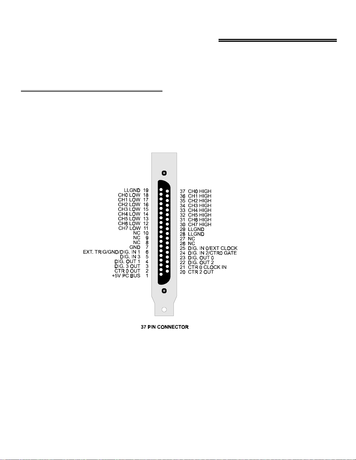
4.1 ANALOG CONNECTOR DIAGRAM
The CIO-DAS16/M1/16 analog connector is a 37 pin D type connector accessible from the rear of the PC through the expansion
backplate. With the exception of the missing D/A signals, the signals available are identical to the CIO-DAS16.
The connector accepts female 37 D type connectors, such as those on the C73FF-2, 2 foot cable with connectors. If frequent changes to
signal connections or signal conditioning is required, please refer to the information on the CIO-TERMINAL or CIO-MINI37 screw
terminal boards.
6

4.2 ANALOG INPUTS
Analog inputs to the CIO-DAS16/M1/16 should be connected in the manner shown in the following sections. Strict attention must be
paid to cabling and grounding of the shield. Failure to cable as shown WILL LIKELY RESULT IN SIGNAL NOISE.
WARNING - PLEASE READ
Here is a good tip. Measure the voltage (difference) between the ground signal at the signal source and the PC. Use
a volt meter and place the red probe on the PC ground and the black probe on the signal ground. If there is a difference of more than 10 volts, do not connect the CIO-DAS16/M1/16 to this signal source because you will not be able
to make any reading. If the difference is more than 20 volts, DO NOT connect this signal to the CIO-DAS16/M1/16
because it will damage the board and possibly the computer.
4.3 CONNECTING SIGNALS TO THE ANALOG INPUTS
Signal wiring to the CIO-DAS16/M1/16 should be done with consideration for the high speed sampling involved. Even if your A/D
pacing rate is not high, the converter is always converting in under 1uS and the internal MUX switching is done at similarly high
speeds. Close attention must be paid to how analog signals are connected to the board.
The CIO-DAS16/M1/16 has 8 differential analog input channels. Each channel has a signal high input and a signal low input. The
measurement made by the A/D is the voltage difference between the LOW and HIGH inputs. Differential inputs have a common mode
range (see application note). The CIO-DAS16/M1/16 may have as much as +11V or -6V of common mode between LLGND and
signal LOW.
4.3.1 KEEP HIGH AND LOW WIRES TOGETHER
Keep the signal wires for a channel together. Ideally they should form a twisted pair. This will aid the differential inputs in rejecting
EMI or RFI noise from your input signal.
4.3.2 SHIELDING
To further protect the input signals from noise, a shield should be employed. Shielded twisted pair cab le is readily available. The shield
should be connected as shown in the diagrams below otherwise ground loops and signals noise may result.
7

4.3 GROUNDED SIGNAL SOURCE
g
p
A grounded signal source is defined as having the signal low referenced to chassis ground. If an instrument has only two poles, HI and
LOW, it is probably referenced to chassis ground internally. It is easy to check with an Ohm meter between LOW and the power cord
ground prong. If an instrument has three poles, a HI, LOW and GND then you may strap LO to GND as shown here, or use the connection for Floating Signal Source.
CIO -DAS16/M1/16
Instrument
Shielded Cable
Signal High
Channel # High
Signal Low
Tie Lo w to GND
GND
GROUNDED SIGNAL SOURCE - Suggested way to connect
signal and cable shield. Ground is completed through
power coards and power lines. Potential between outlet
grounds not to exceed the common mode range.
4.3.4 FLOATING SIGNAL SOURCE
A floating signal source is defined as having the signal low with no reference to earth ground (PC Chassis ground or LLGND).
Examples are a battery, an isolated precision power supply or a sensor which is not earth grounded.
A reference between signal LOW and LLGND must be provided because the CIO-DAS16/M1/16 inputs are differential. Failure to
supply the reference (10K resistor) will result in unrepeatable readings.
Channel # Low
LLGND
CIO-DAS16/M1/16
Shielded Cable
Signal High
Signal Low
Channel # High
Channel # Low
LLGN D
FLOATING SIGNAL SOURCE - Suggested way to c o nn e ct s ignals
an d cable sh ield . C onne c ti on is made t o Ea rt h
round through
ower cord.
8

4.3.5 AVOIDING GROUND LOOPS
This is a diagram of how to connect to a grounded signal the wrong way and create a gr ound loop. The current flowing through the
ground will be sufficient to interfere with your reading as will the voltage potential between the grounds.
CIO-DAS16/M1/16
Shielded Cable
Signal High
Channel # High
Signal Low
Ground Loop
Created Here
WRONG WAY! - This is the wrong way to connect signal and
cable shield.
Channel # Low
LLGND
DO NOT HOOK UP THIS WAY!
4.4 DIGITAL OUTPUTS & INPUTS
All the digital outputs and inputs on main I/O connector are TTL level. TTL is an electronics industry term, short for Transistor
Transistor Logic, which describes a standard for digital signals which are either at 0V or 5V. The binary logic inside the PC is all TTL
or LSTTL (Low power Schotky TTL).
If you desire to control or sense any device other than TTL IC chips, please use appropriate signal conditioning, such as solid state
relays or electromechanical relays. See the catalog for SSR-RACK24 and CIO-ERB24 interface accessories.
9

4.5 24 DIGITAL I/O CONNECTOR
A second connector at the rear of the board contains signals from one 82C55. These 24 bits of digital I/O (82C55) are available for
on/off control, switch condition monitoring or other digital interface tasks. The connector and register alignment is identical to that of
the CIO-DIO24.
The 40 pin header at the rear of the CIO-DAS16/M1/16 is pinned out such that when connected to a 37 pin connector via a BP40-37,
the 37 pin connector's pinouts are identical to that of the CIO-DIO24. We recommend that you purchase and use a BP40-37 if you
desire access to the 24 bits of digital I/O and 3 counters on the rear connector.
Shown here is the pin out of a BP40-37 connected to the digital/connector.
4.6 DT-CONNECT
There is no hardware configuration or installation required for DT-Connect. Software enables/disables DT-Connect, and of course, you
must have a DT-Connect equipped accessory board before using the DT-Connect.
4.6.1 DT-CONNECT IN MASTER MODE ONLY
The CIO-DAS16/M1/16 implements DT-Connect MASTER MODE only. DT-Connect is always enabled and is never busy. The
ENABLED and BUSY signal levels are fixed in hardware. Since DT-Connect is always enabled, any A/D conversions are always transferred out the DT-Connect regardless of the bus transfer method specified. The CIO-DAS16/M1/16 can only operate in DT-Connect
schemes where it is the sole master.
To assure that DT-Connect is properly initialized prior to any A/D transfer, the DT-Connect DT-Request handshake line is reset each
time the programmable gain (Base + 11) register is written to. Therefore, it is not possible to use the DT-Connect for A/D sets which
involve setting the gain between samples. This is not really a problem because any such scheme would be low speed and therefore store
data to disk, obviating the need to use DT-Connect to store data on a memory board.
Please see the data sheet on the MEGA-FIFO, TheWO 128 million sample buffer board as an example of a DT-Connect
accessory.
10

5 SOFTWARE
There are three common approaches to software for the CIO-DAS16/M1/16. These are: Writing custom software utilizing our Universal
Library package, using a fully integrated software package (e.g. Labtech Notebook), or direct register level programming.
5.1 CUSTOM SOFTWARE UTILIZING THE UNIVERSAL LIBRARY
Most customers write custom software using UniversalLibrary. The Universal Library takes care of all the board I/O commands and lets
you concentrate on the application part of the software. For additional information regarding using the Universal Library, please refer to
the documentation supplied with the Universal Library.
Insta
acquisition board. InstaCal also creates a configuration file required for programmers who use the Universal Library.
TM
is a complete installation, calibration and test package. Use it to guide the installation procedure and to calibrate your data
Cal
5.2 FULLY INTEGRATED SOFTWARE PACKAGES (e.g. HP VEE)
Many customers also take advantage of the power and simplicity offered by one of the upper level data acquisition packages. Please
refer to the package’s documentation for setup and usage details.
5.3 DIRECT REGISTER LEVEL PROGRAMMING
Though uncommon, so me applicat ions do not allow the use o f our Universal Librar y, and are not a good match for an upper level
package. For these sophisticated programmers, we provide a detailed register mapping in Chapter 5.
11

6.1 DAS16/M1/16 REGISTER MAP
6 CIO-DAS16/M1/16 REGISTER MAP
WRITE FUNCTIONREAD FUNCTIONADDRESS
Software Start A/D ConversionA/D Data - 16 bits BASE
Not UsedNot UsedBASE + 1
Channel Mux read/Reset FIFOChannel Mux SetBASE + 2
Digital Output Bits 0-3ID, Digital In 0-3, External ControlBASE + 3
Not UsedNot UsedBASE + 4
Not UsedNot UsedBASE + 5
Not UsedNot UsedBASE + 6
Not UsedNot UsedBASE + 7
Clear the interruptStatus, Mux settingBASE + 8
Interrupt selection, Pacer/triggerInterrupt Enable/select, Pacer/triggerBASE + 9
Burst Length, Trigger, CTR0/TRG0 Burst Length, Trigger, CTR0/TRG0BASE + 10
Gain/Range Control, Res CTRGain/Range status, FFNE, Res CTRBASE + 11
Counter 0 Data - Residual CounterCounter 0 Data - Residual CounterBASE +12
Counter 1 Data - A/D PacerCounter 1 Data - A/D Pacer ClockBASE +13
Counter 2 Data - A/D PacerCounter 2 Data - A/D Pacer ClockBASE + 14
Pacer Clock (8254) ControlNone. No read back on 8254BASE +15
8255 Port A Data8255 Port A DataBASE+400h
8255 Port B Data8255 Port B DataBASE+401h
8255 Port C Data8255 Port C DataBASE+402h
8255 Control RegisterNo 8255 Read-backBASE+403h
DAS16/M1/16 REGISTER DESCRIPTION
The CIO-DAS16/M1/16 register map shown above is 8-bit transfers, except for BASE + 1 which is the A/D data register which is
16-bit transfers only. This allows for high-speed REP-INSW operation.
6.2 A/D DATA WORD REGISTER
BASE + 0 Example, 300 HEX, 768 Decimal
0132456789101112131415
AD15
MSB
A read/write register. The A/D Data Register is configured as a word because REP INSW can be used to quickly read data from the
board, allowing for higher A/D conversion rates than would be possible if using DMA, which accesses the A/D data as two bytes.
AD1AD2AD3AD4AD5AD6AD7AD8AD9AD10AD11AD12AD13AD14
AD0
LSB
12

READ
On read, the 16-bit ADC value is presented in 'left-justified' format, with the Most-significant ADC bit occupying the data word bit
position #15; the lease significant ADC bit occupies bit position #0 of the data word.
WRITE
A write to the base address will cause an A/D conversion, (Bits 0&1 of BASE+9 must be 0.)
Also, the write to base address acts as an Internal Trigger to start conversions if the method of converting is External or Internal Pacer.
6.3 CHANNEL MUX HI/LO LIMITS WORD REGISTER
BASE ADDRESS +2 Example, 302 HEX, 770 Decimal
01324567
CH1LCH2LCH4LCH8LCH1HCH2HCH4HCH8H
This register functions the same as DAS1600 products in 8 channel differential mode. The channel mux setting is written and read from
in this register. To configure the channels to convert, the upper nibble sets the high channel and the lower nibble sets the low channel.
For example:
- To sample channel 1 only, write 11 hex to BASE+2
- To sample channels 0 - 2, write 20 hex to BASE+2
- To sample channels 5 and 6, write to 65 hex to BASE+2
WRITE
Sets the channel mux and resets the FIFO.
READ
Reads the current channel mux which the A/D will convert on the next trigger pulse.
6.4 8-BIT DIGITAL I/O REGISTERS
BASE ADDRESS +3 Example, 303 HEX, 771 Decimal
READ
01324567
DI30011
The 4 digital inputs and the upper nibble of the board ID, and are read as one byte. Three of the pins have special functions in addition
to being digital input pins. They are:
ExtPacer/DI0 External Pacer: Single A/D conversion on each active edge.
ExtTrig/DI1 External Trigger/Gate: Starts Pacer (Internal/External) which generates A/D Conversions on each active
edge of pacer.
GATE0/DI2 Gate for CTR0 Used to Gate Counter 0.
WRITE
DI2
GATE0
DI1
ExtTrig
DI0
ExtPacer
01324567
DO0DO1DO2DO3Not UsedNot UsedNot UsedNot Used
All of the 4 bits are latched TTL outputs.
The WRITE to this register also clears external trigger latched bit.
13

6.5 STATUS REGISTER
BASE ADDRESS + 8 Example, 308 HEX, 776 Decimal
READ
Description of Status Register read bits:
EOC
- End of Conversion. 1 = Busy, 0 = Conversion complete.
U/B
- Unipolar/Bipolar. 0 = Bipolar A/D input, 1 = Unipolar A/D input.
OVRN
- FIFO Overrun status. 0 = has not overrun (not full), 1 = overrun (FIFO is full).
(The OVRN bit is latched. The latch is cleared by a FIFO clear write to Base + 2).
INTB
- State of interrupt flop. Latched. 0 = no interrupt occurred, 1 = interrupt occurred.
MA3:0
WRITE
The write function clears the interrupt.
- Current channel mux setting for next conversion.
6.6 INTERRUPT AND PACER CONTROL REGISTER
01234567
MA0MA1MA2MA3INTB OVRNU/B EOC
BASE ADDRESS +9 Example, 309 HEX, 777 Decimal
READ/WRITE
01234567
TS0TS1-BMDEINT1INT2INT4INT8
Burst Mode is a method of performing pseudo-simultaneous sample-and-hold on a specified number of channels without using an external sample-and-hold board or providing individual sample-and-hold amplifiers or A/D converters on each channel. For the
DAS16/M1/16, when Burst Mode is selected, each channel in the burst will be sampled at the maximum speed of the A/D converter - 1
MHz - and the time between bursts is set by TS1:0. The channels contained in the burst are set by register BASE+2 and the number of
channels in the burst are set by register BASE+10.
The interrupts are enabled/disabled and selected using the following 4 bits. The routing of the interrupts is set by the TS0/TS1 bits.
When TS1 is set to 1 (not Software conversions), the interrupt is generated by FIFO Half Full. That is, when the A/D is sampling and
reaches 512 samples, this interrupt is generated to allow the user to perform a REP INSW block transfer. When TS0 and TS1 are set to
0, Software triggers are enabled in Low Speed Mode and the interrupts are generated at the end of each FIFO write. That is, when a
sample of data is written into the FIFO an interrupt is generated to allow the user to read it. Finally, when performing REP INSW, if
the number of samples is not a 512 block multiple, there will be a residual number of samples to be taken. By setting the Enhanced bit
(register Base + 11), when RCG is set, the residual samples are to be taken and the interrupts are generated from the residual counter Counter 0 (see Base + 11 for further description).
14

INT4:1 - Interrupt selection
INTERRUPTINT1INT2INT4INT8
DISABLED0000
Not Available1000
20100
31100
40010
51010
60110
71110
Not Available0001
Not Available1001
100101
111101
120011
Not Available1011
140111
151111
BMDE - Burst Mode Enable. 0 = disable, 1 = enabled. The number of channels in the burst are set in BASE+10 register.
TS1:0 - A/D trigger source
TRIGGER SOURCETS0TS1
Software TriggerX0
Rising External Pacer 01
Internal Paced 11
To perform conversions in Software Mode, the A/D converter samples at 1 MHz. The maximum delay from the trigger to the first 1
MHz convert pulse is < 1 uSec, since the trigger enables the 1 MHz pulse train to pass through to the counter circuit to count 3 pulses
which in turn will generate the FIFO write pulse. Therefore, the maximum delay from the Software Trigger (Base + 0 Write) is 3 uSec.
To perform conversions in Pacer modes, the following sequence must be followed by the program:
The counter (Internal Paced) or DIN0 (External Paced) must be set.
Set the Pacer generator, TS1/0, appropriately.
To initiate the conversions, perform a WRITE to Base + 0 (as in Software Mode) or set an external trigger/gate.
To stop conversions, perform a Base + 9 Write cycle. If using an external trigger, the clearing of the trigger pulse will end conversions.
6.7 BURST LENGTH, EXTERNAL TRIGGER, CTR0/TRG0
BASE ADDRESS +10 Example, 30A HEX, 778 Decimal
READ/WRITE
01234567
TRG0CTR0TRGSELTRGPOLBL0BL1BL2BL3
15

BL3:0 - Burst Length. The number of channels in the burst are set by BL3:0, where the channels that are contained in the burst are set
by register BASE+2. For example:
- To perform a channel burst conversion on channels 0 - 2, set BASE+2 to 20 hex and the upper nibble of BASE+10 to 3.
TRGPOL - Trigger polarity. 0 = rising trigger/high gate, 1 = falling trigger/low gate.
TRGSEL - Trigger select. 0 = Gate - generate conversions while signal is active, 1 = Trigger - single edge to initiate conversions.
CTR0 - Counter 0 control. 0 = external clock input to counter 0, 1 = internal 1 MHz input.
TRG0 - Trigger enable. 0 = Gates for counters 1 and 2 enabled preventing external triggers, 1 = external trigger enabled allowing
rising edge to trigger counter (A/D converter).
6.8 COUNTER, GAIN/RANGE CONTROL
BASE ADDRESS +11 Example, 30B HEX, 779 Decimal
READ/WRITE
01234567
G0G1U/BFFNE*RCGEnhancedNot UsedNot Used
* Read Only
Enhanced Mode and RCG bits are used in REP INSW conversion mode to allow the correct number of samples to be taken. In REP
INSW, an interrupt is generated every 512 samples at which point the REP INSW function is used to perform a block transfer of the
512 samples. When the number of samples to be taken is not a multiple of 512, the final interrupt would never be generated. Therefore,
a mechanism has been implemented allowing the software to know how many samples are left in the FIFO. The Residual Counter
functions as follows:
The software knows how many samples the user wants to convert, and divides this number by 512 (the number of samples in a REP
INSW block) - this will be the total number of interrupts generated by the FIFO. The remaining number of samples is written to
Counter 0.
The user then starts conversions, taking interrupts every 512 sample blocks. When the number of interrupts is 1 less than the total,
software will set the RCG bit. When the last interrupt is generated, each subsequent conversion counts down Counter 0 until it reaches
terminal count, at which time the final interrupt is generated to read off remaining samples.
ENHANCED - Enhanced Mode. Enhanced Mode is used to enable Counter 0 to function as the residual counter, disconnecting it from
being a general purpose counter to the user. 0 = default, 1 = Enhanced mode.
RCG - Residual Counter Gate. 0 = disabled, 1 = enabled. The Residual Counter Gate gates Counter 0 'on' to allow the software to
count the residual number of samples taken off the FIFO in REP INSW mode.
FFNE - FIFO Not Empty. 0 = FIFO is not empty - contains A/D data, 1 = FIFO is empty.
UNI/BIP - A/D input Unipolar/Bipolar mode select. 0 = Bipolar mode, 1 = Unipolar mode.
G1:0 - A/D input Gain setting.
ANALOG INPUT VOLTAGE RANGEANALOG INPUT GAING0G1
0-10V or ±5V100
0-5V or ±2.5V210
0-2.5V or ±1.25V401
0-1.25V or ±.625V811
16

6.9 8254 DATA AND CONTROL REGISTERS
6.9.1 8254 COUNTER 0 DATA - GENERAL PURPOSE OR RESIDUAL COUNTER
BASE + 12 Example, 30C hex, 780 decimal
READ/WRITE
01324567
D1D2D3D4D5D6D7D8
In default mode, Counter 0 is a general purpose counter supplied to the user. When REP INSW conversions are performed and the user
sets Enhanced Mode, Counter 0 becomes a residual counter (See register Base + 11 for further description).
*NOTE: Total count must be greater than 512 for the residual counter to work correctly.
6.9.2 8254 COUNTER 1 DATA - PACER DIVIDER LOWER
BASE + 13 Example, 30D hex, 781 decimal
READ/WRITE
01324567
D1D2D3D4D5D6D7D8
6.9.3 8254 COUNTER 2 DATA - PACER DIVIDER UPPER
BASE + 14 Example, 30E hex, 782 decimal
READ/WRITE
01324567
D1D2D3D4D5D6D7D8
Counter 1 is the lower 16 bits of the 32-bit pacer clock divider. It's output is fed to the clock input of Counter 2 which is the upper
16-bits of the pacer clock divider. The clock input to Counter 1 is a 10 MHz precision oscillator source.
Counter 2's output is called the 'Internal Pacer' and can be selected by software to be the A/D Pacer source. Counters 1 & 2 should be
configured to operate in 8254 Mode 2.
6.9.4 8254 CONTROL REGISTER
BASE + 15 Example, 30F hex, 783 decimal
WRITE ONLY
01324567
D1D2D3D4D5D6D7D8
The control register is used to set the operating Modes of 8254 Counters 0,1 & 2. A counter is configured by writing the correct Mode
information to the Control Register, then the proper count data must be written to the specific Counter Register.
The Counters on the 8254 are 16-bit devices. Since the interface to the 8254 is only 8-bits wide, Count data is written to the Counter
Register as two successive bytes. First the low byte is written, then the high byte. The Control Register is 8-bits wide. Further information can be obtained on the 8254 data sheet, available from Intel or Harris.
17

6.10 8255 DIGITAL I/O DATA AND CONTROL REGISTERS
The 8255 Digital I/O port is at Register BASE+400hex to follow the register configuration of the CIO-DAS1600 family.
6.10.1 8255 PORT A DATA
BASE + 400hex Example, 700 hex, 1792 decimal
READ/WRITE
6.10.2 8255 PORT B DATA
BASE + 401hex Example, 701 hex, 1793 decimal
READ/WRITE
6.10.3 8255 PORT C DATA
BASE + 402hex Example, 702 hex, 1794 decimal
READ/WRITE
01324567
D1D2D3D4D5D6D7D8
01324567
D1D2D3D4D5D6D7D8
01324567
D1D2D3D4D5D6D7D8
6.10.4 8255 CONTROL REGISTER
BASE + 403hex Example, 703 hex, 1795 decimal
WRITE ONLY
01324567
D1D2D3D4D5D6D7D8
The control register is used to set the operating Modes of 8255 Ports A, B, and C. A port is configured by writing the correct Mode
information to the Control Register, then the proper data must be written to the specific digital output register or read from the specific
input register. Further information can be obtained on the 8255 data sheet, available from Intel or Harris.
WRITE FUNCTIONREAD FUNCTIONADDRESS
Port A OutputPort A Input of 82C55 BASE + 400
Port B OutputPort B InputBASE + 401
Port C OutputPort C InputBASE + 402
Configure 82C55 None. No read back on 82C55BASE + 403
18

The two groups of ports, group A and group B, may be independently programmed in one of several modes. The most commonly used
mode is mode 0, input / output mode. The codes for programming the 82C55 in this mode are shown below. D7 is always 1 and D6,
D5 & D2 are always 0.
CLBCUADECHEXD0D1D3D4
OUTOUTOUTOUT128800000
INOUTOUTOUT129811000
OUTINOUTOUT130820100
ININOUTOUT131831100
OUTOUTINOUT136880010
INOUTINOUT137891010
OUTININOUT1388A0110
INININOUT1398B1110
OUTOUTOUTIN144900001
INOUTOUTIN145911001
OUTINOUTIN146920101
ININOUTIN147931101
OUTOUTININ152980011
INOUTININ153991011
OUTINININ1549A0111
ININININ1559B1111
19

7 CALIBRATION AND TEST
Every board was fully tested and calibrated before being placed in finished goods inventory at the factory. For normal environments a
calibration interval of 6 months to one year is recommended. If frequent variations in temperature or humidity are common then recalibrate at least once every three months. It takes less than 30 minutes to calibrate the CIO-DAS16/M1/16.
7.1 REQUIRED EQUIPMENT
You will will need a precision voltage source and a few pieces of wire.
You will not need an extender card to calibrate the board b ut you will need to have the cover off your computer with the power on, so
trim pots can be adjusted during calibration. For that reason a plastic screwdriver has been supplied with your CIO-DAS16/M1/16. In
the event that the screwdriver is dropped into the PC, no damage will result from short circuits.
7.2 CALIBRATING THE A/D CONVERTERS
The A/D is calibrated by applying a known voltage to an analog input channel and adjusting trim pots for offset and gain. There are
two trim pots requiring adjustment to calibrate the analog input section of the CIO-DAS16/M1/16. The entire procedure is described in
detail in the Insta
TM
, calibration routine.
Cal
The CIO-DAS16/M1/16 should be calibrated for the range you intend to use it in. When the range is changed, slight variation in Zero
and Full Scale may result. These variations can be measured and removed in software if necessary.
20

8 SPECIFICATIONS
Analog input section
A/D converter type Datel ADS-30356 Subranging
Resolution 16 bits
Programmable ranges ±5V, ±2.5V, ±1.25V,±.625V, 0 - 10V, 0 - 5V, 0 - 2.5V, 0 - 1.25V
A/D pacing Programmable: internal counter or external source (Din0, rising edge) or software
polled
Burstmode intersample time 1 µs
Data transfer Word wide from 1ksample FIFO via REP INSW, interrupt, DT Connect or software
polled
Polarity Unipolar/Bipolar software selectable, 10mS delay switching
Number of channels 8 differential
A/D Trigger sources External trigger/gate (DIN1)
A/D Triggering Modes
Digital: Software configurable for edge (triggered) or level-activated (gated). Programmable
polarity (rising/falling edge trigger, high/low gate).
A/D conversion time 1 µs
Throughput 1 MHz max
Differential Linearity error ±1 LSB max
Integral Linearity error ±6 LSB max
Offset Error ±10 LSB max
Common Mode Range +11V, -6V
CMRR (60Hz, Vin = CMR) 90dB
1
No missing codes guaranteed 16 bits
Gain drift (A/D specs) ±30ppm/°C, all ranges
Input leakage current (@25 Deg C) < 200nA
Input impedance Min 10Meg Ohms
Absolute maximum input voltage ±15V
Digital Input / Output
Digital Type (Main Connector)
Input: 74LS244
Output: 74LS197
Configuration Two dedicated ports, 4 input and 4 output
Output High 2.7 volts @ -.4mA min
Output Low 0.4 volts @ 8 mA min
Input High 2.0 volts min, 7 volts absolute max
Input Low 0.8 volts max, -0.5 volts absolute min
Digital Type (Auxiliary Connector) 82C55
Configuration 2 banks of 8, 2 banks of 4, programmable by bank as input or output
Output High 3.0 volts min @ -2.5mA
Output Low 0.4 volts max @ 2.5mA
Input High 2.0 volts min, 5.5 volts absolute max
Input Low 0.8 volts max, -0.5 volts absolute min
Interrupts Programmable levels 2-7, 10-12, 14, 15; Positive edge triggered
Interrupt enable Programmable
Interrupt sources A/D End-of-conversion, A/D FIFO half full, A/D Residual Counter
1
Offset error can be trimmed to zero by adjusting the offset potentiometer for zero offset at the sampling frequency to be used.
21

Counter section
Counter type 82C54
Configuration 3 down counters, 16 bits each
Counter 0 - General purpose counter or ADC residual sample counter when using
REPINSW.
Source: Programmable: external (CTR0IN), internal (1MHz osc) or ADC
pacer(when using REPINSW).
Gate: Programmable source: external (DIN2) or internal (when using
REPINSW)
Output: Programmable: user connector, end-of-acquisition interrupt (when
using REPINSW).
Counter 1 - ADC Pacer Lower Divider
Source: 10 MHz oscillator
Gate: Tied to Counter 2 gate, programmable source: external (DIN1) or
internal.
Output: Chained to Counter 2 Clock.
Counter 2 - ADC Pacer Upper Divider
Source: Counter 1 Output.
Gate: Tied to Counter 1 gate, programmable source: external (DIN1) or
internal.
Output: ADC Pacer clock, output available at user connector (CTR2 Out).
Clock input frequency 10Mhz max
High pulse width (clock input) 30ns min
Low pulse width (clock input) 50ns min
Gate width high 50ns min
Gate width low 50ns min
Input low voltage 0.8V max
Input high voltage 2.0V min
Output low voltage 0.4V max
Output high voltage 3.0V min
Environmental
Operating temperature range 0 to 60°C
Storage temperature range -40 to 100°C
Humidity 0 to 90% non-condensing
Power consumption
+5V: Operating 2.25 A typ / 2.9 A max
All Specifications typical for 25 DegC unless otherwise specified.
22

Declaration of Conformity
DescriptionPart number
High-speed analog input boardCIO-DAS16/M1/16
to which this declaration relates, meets the essential requirements, is in conformity with, and CE marking has been applied according to
the relevant EC Directives listed below using the relevant section of the following EC standards and other normative documents:
EU EMC Directive 89/336/EEC
EU 55022 Class B
EN 50082-1
IEC 801-2
IEC 801-3
IEC 801-4
Carl Haapaoja, Director of Quality Assurance
: Electrostatic discharge requirements for industrial process measurement and control equipment.
: Radiated electromagnetic field requirements for industrial process measurements and control equipment.
: Electrically fast transients for industrial process measurement and control equipment.
: Limits and methods of measurements of radio interference characteristics of information technology equipment.
: EC generic immunity requirements.
: Essential requirements relating to electromagnetic compatibility.
23

24
 Loading...