

Page 1
AD590JFAD590JF AD590KF
User’s Guide
Shop online at
AD590JH AD590KH
omega.com
e-mail: info@omega.com
For latest product manuals:
omegamanual.info
AD590
Temperature Sensors
Page 2

OMEGAnet®Online Service Internet e-mail
omega.com info@omega.com
Servicing North America:
U.S.A.: One Omega Drive, P.O. Box 4047
ISO 9001 Certified Stamford, CT 06907-0047
TEL: (203) 359-1660
FAX: (203) 359-7700
e-mail: info@omega.com
Canada: 976 Bergar
Laval (Quebec) H7L 5A1, Canada
TEL: (514) 856-6928
FAX: (514) 856-6886
e-mail: info@omega.ca
For immediate technical or application assistance:
U.S.A. and Canada: Sales Service: 1-800-826-6342/1-800-TC-OMEGA
Customer Service: 1-800-622-2378/1-800-622-BEST
Engineering Service: 1-800-872-9436/1-800-USA-WHEN
Mexico: En Espan˜ ol: (001) 203-359-7803
e-mail: espanol@omega.com
FAX: (001) 203-359-7807
info@omega.com.mx
®
®
®
Servicing Europe:
Czech Republic: Frystatska 184, 733 01 Karviná, Czech Republic
TEL: +420 (0)59 6311899
FAX: +420 (0)59 6311114
Toll Free: 0800-1-66342
e-mail: info@omegashop.cz
Germany/Austria: Daimlerstrasse 26, D-75392 Deckenpfronn, Germany
TEL: +49 (0)7056 9398-0
FAX: +49 (0)7056 9398-29
Toll Free in Germany: 0800 639 7678
e-mail: info@omega.de
United Kingdom: One Omega Drive, River Bend Technology Centre
ISO 9002 Certified Northbank, Irlam, Manchester
M44 5BD United Kingdom
TEL: +44 (0)161 777 6611
FAX: +44 (0)161 777 6622
Toll Free in United Kingdom: 0800-488-488
e-mail: sales@omega.co.uk
It is the policy of OMEGA Engineering, Inc. to comply with all worldwide safety and EMC/EMI
regulations that apply. OMEGA is constantly pursuing certification of its products to the European Ne
Approach Directives. OMEGA will add the CE mark to every appropriate device upon certification
The information contained in this document is believed to be correct, but OMEGA accepts no liability for any
errors it contains, and reserves the right to alter specifications without notice.
WARNING: These products are not designed for use in, and should not be used for, human applications.
.
w
Page 3

2-Terminal IC
–
Temperature Transducer
FEATURES
Linear current output: 1 µA/K
Wide temperature range: −55°C to +150°C
Pr
obe-compatible ceramic sensor package
2-terminal device: voltage in/current out
Laser trimmed to ±0.5°C calibration accuracy (AD590M)
Excellent linearity: ±0.3°C over full range (AD590M)
Wide power supply range: 4 V to 30 V
isolation from case
Sensor
Low cost
GENERAL DESCRIPTION
e AD590 is a 2-terminal integrated circuit temperature
tran
sducer that produces an output current proportional to
absolute temperature. For supply voltages between 4 V and
V, the device acts as a high impedance, constant current
30
regulator passing 1 µA/K. Laser trimming of the chip’s thin-film
resistors is used to calibrate the device to 298.2 µA output at
298
.2 K (25°C).
e
AD590 should be used in any temperature-sensing
application below 150°C in which conventional electrical
temperature sensors are currently employed. e inherent
low cost of a monolithic integrated circuit combined with the
elimination of support circuitry makes the AD590 an attractive
alternative for many temperature measurement situations.
Linearization circuitry, precision voltage amplifiers, resistance
measuring circuitry, and cold junction compensation are not
needed in applying the AD590.
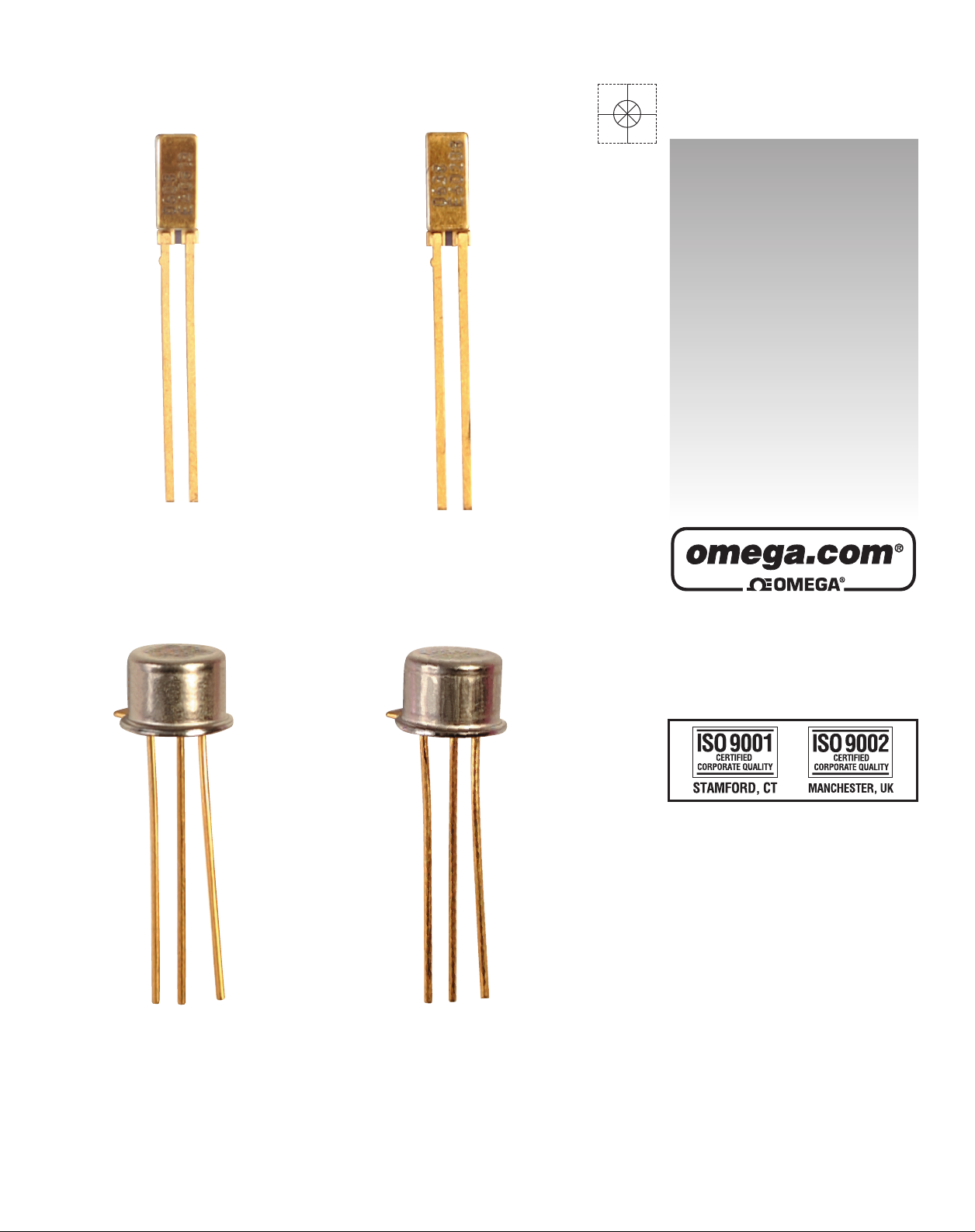
AD590
PIN CONFIGURATIONS
NC
1
2
V+
TOP VIEW
(Not to Scale)
V–
3
4
420-3
3
500
+ –
Fi
gure 1. 2-Lead CQFP Figure 2. 8-Lead SOIC
+
gure 3. 3-Pin TO-52
Fi
5
2
0-
3
35
0
NC
NC = NO CONNECT
PRODUCT HIGHLIGHTS
1. e AD590 is a calibrated, 2-terminal temperature sensor
requiring only a dc voltage supply (4 V to 30 V). Costly
transmitters, filters, lead wire compensation, and linearization
ci
rcuits are all unnecessary in applying the device.
2. State-of-the-art laser trimming at the wafer level in
conjunction with extensive final testing ensures that
AD
590 units are easily interchangeable.
NC
8
7
NC
NC
6
5
NC
100
33500
In addition to temperature measurement, applications include
temperature compensation or correction of discrete components,
biasing proportional to absolute temperature, flow rate
measurement, level detection of fluids and anemometry.
e
AD590 is available in chip form, making it suitable for
hybrid circuits and fast temperature measurements in
protected environments.
e AD590 is particularly useful in remote sensing applications.
e
device is insensitive to voltage drops over long lines due to
its high impedance current output. Any well-insulated twisted
pair is sufficient for operation at hundreds of feet from the
receiving circuitry. e output characteristics also make the
easy to multiplex: the current can be switched by a
AD590
3. Superior interface rejection occurs because the output is a
current rather than a voltage. In addition, power
requirements are low (1.5 mW @ 5 V @ 25°C). ese
features make the AD590 easy to apply as a remote sensor.
4. e high output impedance (>10 MΩ) provides excellent
rejection of supply voltage dri and ripple. For instance,
ging the power supply from 5 V to 10 V results in only
chan
a 1 µA maximum current change, or 1°C equivalent error.
5. e AD590 is electrically durable: it withstands a forward
voltage of up to 44 V and a reverse voltage of 20 V.
e
refore, supply irregularities or pin reversal does not
damage the device.
CMOS multiplexer, or the supply voltage can be switched by a
lo
gic gate output.
Page 4

AD590
TABLE OF CONTENTS
Features.............................................................................................. 1
Ge
neral Description ......................................................................... 1
Explanation of Temperature Sensor Specifications ..................7
Calibration Error...........................................................................7
Configurations ...........................................................................1
Pin
Product Highlights ........................................................................... 1
Revision History ............................................................................... 2
Specifications..................................................................................... 3
AD590J
AD590L
Absolute Maximum Ratings............................................................ 5
ESD Caution.................................................................................. 5
Ge
Circuit Description....................................................................... 6
and AD590K Specifications ......................................... 3
and AD590M Specifications ....................................... 4
neral Description ......................................................................... 6
Error vs. Temperature: with Calibration Error Trimmed
Out...................................................................................................7
Error vs. Temperature: No User Trims .......................................7
Nonlinearity...................................................................................7
Voltage and ermal Environment Effects ...............................8
General Applications...................................................................... 10
Outline Dimensions....................................................................... 13
Page 2 of 16
Page 5

AD590
SPECIFICATIONS
AD590J AND AD590K SPECIFICATIONS
25°C and VS = 5 V, unless otherwise noted.
Table 1.
AD590J AD590K
Parameter Min Typ Max Min Typ Max Unit
POWER SUPPLY
Operating Voltage Range
OUTPUT
Nominal Current Output @ 25°C (298.2K) 298.2 298.2 µA
Nominal Temperature Coefficient 1 1 µA/K
Calibration Error @ 25°C
Absolute Error (Over Rated Performance Temperature Range)
Without External Calibration Adjustment
With 25°C Calibration Error Set to Zero
Nonlinearity
For TO-52 and CQFP Packages
For 8-Lead SOIC Package
Repeatability
Long-Term Drift
2
3
Current Noise 40 40
Power Supply Rejection
4 V ≤ VS ≤ 5 V 0.5 0.5 µA/V
5 V ≤ VS ≤ 15 V 0.2 0.2 µV/V
15 V ≤ VS ≤ 30 V 0.1 0.1 µA/V
Case Isolation to Either Lead 10
Effective Shunt Capacitance 100 100 pF
Electrical Turn-On Time 20 20 µs
Reverse Bias Leakage Current (Reverse Voltage = 10 V)
1
Specifications shown in boldface are tested on all production units at final electrical test. Results from those tests are used to calculate outgoing quality levels. All
minimum
2
Maximum deviation between +25°C readings after temperature cycling between −55°C and +150°C; guaranteed, not tested.
3
Conditions: constant 5 V, constant 125°C; guaranteed, not tested.
4
Leakage current doubles every 10°C.
and maximum specifications are guaranteed, although only those shown in boldface are tested on all production units.
1
4
30
±5.0
±10
±3.0
±1.5
±1.5
4
30 V
±2.5
±5.5
±2.0
±0.8
±1.0
°C
°C
°C
°C
°C
±0.1 ±0.1 °C
±0.1 ±0.1 °C
pA/√Hz
10
10
4
10 10 pA
10
Ω
Page 3 of 16
Page 6
AD590
K°C
AD590L AND AD590M SPECIFICATIONS
25°C and VS = 5 V, unless otherwise noted.
Table 2.
AD590L AD590M
Parameter Min Typ Max Min Typ Max Unit
POWER SUPPLY
Operating Voltage Range 4 30 4 30 V
OUTPUT
Nominal Current Output @ 25°C (298.2K) 298.2 298.2 µA
Nominal Temperature Coefficient 1 1 µA/K
Calibration Error @ 25°C ±1.0 ±0.5 °C
Absolute Error (Over Rated Performance Temperature Range) °C
Without External Calibration Adjustment ±3.0 ±1.7 °C
With ± 25°C Calibration Error Set to Zero ±1.6 ±1.0 °C
Nonlinearity ±0.4 ±0.3 °C
Repeatability
Long-Term Drift
2
3
Current Noise 40 40 pA/√Hz
Power Supply Rejection
4 V ≤ VS ≤ 5 V 0.5 0.5 µA/V
5 V ≤ VS ≤ 15 V 0.2 0.2 µA/V
15 V ≤ VS ≤ 30 V 0.1 0.1 µA/V
Case Isolation to Either Lead 10
Effective Shunt Capacitance 100 100 pF
Electrical Turn-On Time 20 20 µs
Reverse Bias Leakage Current (Reverse Voltage = 10 V)
1
Specifications shown in boldface are tested on all production units at final electrical test. Results from those tests are used to calculate outgoing quality levels. All
minimum and maximum specifications are guaranteed, although only those shown in boldface are tested on all production units.
2
Maximum deviation between +25°C readings after temperature cycling between –55°C and +150°C; guaranteed, not tested.
3
Conditions: constant 5 V, constant 125°C; guaranteed, not tested.
4
Leakage current doubles every 10°C.
1
±0.1 ±0.1 °C
±0.1 ±0.1 °C
10
10
4
10 10 pA
10
Ω
+223°
°
°F
–50
°
–100° 0° +100° +200° +300°
Figure 4. Temperature Scale Conversion Equations
+273°0°+298°
+32° +70° +212°
5
9
9
°F = °C + 32)
5
+25°
(
(
+323°
+50°
32)
+373°
+100°
+ 273.15°C = °F – K = °C
+423°
+150°
2
0
0
3
3
5
00
+ 459.7R = °F
Page 4 of 16
Page 7

AD590
ABSOLUTE MAXIMUM RATINGS
Table 3.
Parameter Rating
Forward Voltage ( E+ or E–) 44 V
Reverse Voltage (E+ to E–) −20 V
Breakdown Voltage (Case E+ or E–) ±200 V
Rated Performance Temperature Range
Storage Temperature Range
Lead Temperature (Soldering, 10 sec) 300°C
1
The AD590 was used at −100°C and +200°C for short periods of
mea
surement with no physical damage to the device. However, the absolute
erro
rs specified apply to only the rated performance temperature range.
1
1
−55°C to +150°C
−65°C to +155°C
ESD CAUTION
ESD (electrostatic discharge) sensitive device. Electrostatic charges as high as 4000 V readily accumulate on
the
human body and test equipment and can discharge without detection. Although this product features
proprietary ESD protection circuitry, permanent damage may occur on devices subjected to high energy
ctrostatic discharges. Therefore, proper ESD precautions are recommended to avoid performance
ele
ation or loss of functionality.
degrad
Stresses above those listed under Absolute Maximum Ratings
may cause permanent damage to the device. is is a stress
rating only and functional operation of the device at these or
any other conditions above those indicated in the operational
section of this specification is not implied. Exposure to absolute
ma
ximum rating conditions for extended periods may affect
device reliability.
Page 5 of 16
Page 8

AD590
(
GENERAL DESCRIPTION
e AD590H has 60 µ inches of gold plating on its Kovar leads
and Kovar header. A resistance welder is used to seal the nickel
cap to the header. e AD590 chip is eutectically mounted to
the header and ultrasonically bonded to with 1 mil aluminum
wire. Kovar composition: 53% iron nominal; 29% ± 1% nickel;
17% ± 1% co
balt; 0.65% manganese max; 0.20% silicon max;
0.10% aluminum max; 0.10% magnesium max; 0.10% zirconium
max; 0.10%
e AD590F is
titanium max; and 0.06% carbon max.
a ceramic package with gold plating on its
Kovar leads, Kovar lid, and chip cavity. Solder of 80/20 Au/Sn
composition is used for the 1.5 mil thick solder ring under the
li
d. e chip cavity has a nickel underlay between the metallization
and the gold plating. e AD590 chip is eutectically mounted in
the chip cavity at 410°C and ultrasonically bonded to with 1 mil
aluminum wire. Note that the chip is in direct contact with the
cer
amic base, not the metal lid. When using the AD590 in die
form, the chip substrate must be kept electrically isolated
(floating) for correct circuit operation.
66
MILS
V+
42MILS
PTAT current.
In this figure, Q8 and Q11 are the transistors that produce the
PTAT voltage. R5 and R6 convert the voltage to current. Q10,
whose collector current tracks the collector currents in Q9 and
Q11,
supplies all the bias and substrate leakage current for the
rest of the circuit, forcing the total current to be PTAT. R5 and
R6
are laser-trimmed on the wafer to calibrate the device at 25°C.
Figure 7 shows the typical V–I characteristic of the circuit at
25°C a
nd the temperature extremes.
Figure 6 is the schematic diagram of the AD590.
+
R1
R2
26
0Ω
1040Ω
Q2
Q1
Q7
SUBSTRATE
R6
82
0Ω
Figure 6
Q5 Q3
C1
R3
5kΩ
26pF
R4
11kΩ
Q10Q9
CH
Q6
–
IP
Q12
R5
146Ω
. Schematic Diagram
Q8
Q4
Q11
40
118
0
33
500
V–
THE AD590 IS AVAILABLE IN LASER-TRIMMED CHIP FORM;
CONSULT THE CHIP CATALOG FOR DETAILS
Fi
gure 5. Metallization Diagram
CIRCUIT DESCRIPTION
1
e AD590 uses a fundamental property of the silicon
transistors from which it is made to realize its temperature
pro
portional characteristic: if two identical transistors are
operated at a constant ratio of collector current densities, r,
then the difference in their base-emitter voltage is (kT/q)(In r).
Because both k (Boltzman’s constant) and q (the charge of an
electron) are constant, the resulting voltage is directly
portional to absolute temperature (PTAT).
pro
In the AD590, this PTAT voltage is converted to a PTAT current
by low temperature coefficient thin-film resistors. e total
current of the device is then forced to be a multiple of this
423
30
0
3350
0
)
A
298
µ
T
U
O
I
218
0 1 2
1
For a more detailed description, see M.P. Timko, “A Two-Terminal IC
Temperature
Dec.
Transducer,” IEEE J. Solid State Circuits, Vol. SC-11, p. 784-788,
1976. Understanding the Specifications–AD590.
3 4
SUPPLY VOLTAGE (V)
. V–I Plot
Figure 7
+150°C
+25°C
–55°C
5 6 3
50
0-3
3
500
0
Page 6 of 16
Page 9

AD590
(
V
EXPLANATION OF TEMPERATURE SENSOR
SPECIFICAT
e way in which the AD590 is specified makes it easy to apply
it in a wide variety of applications. It is important to understand
the meaning of the various specifications and the effects of the
suppl
y voltage and thermal environment on accuracy.
AD590 is a PTAT1 current regulator. at is, the output
e
current is equal to a scale factor times the temperature of the
sensor in degrees Kelvin. is scale factor is trimmed to 1 µA/K
at the factory, by adjusting the indicated temperature (that is,
the output current) to agree with the actual temperature. is is
done with 5 V across the device at a temperature within a few
de
grees of 25°C (298.2K). e device is then packaged and
tested for accuracy over temperature.
IONS
CALIBRATION ERROR
At final factory test, the difference between the indicated
temperature and the actual temperature is called the calibration
error. Since this is a scale factory error, its contribution to the
total error of the device is PTAT. For example, the effect of the
1°C
specified maximum error of the AD590L varies from 0.73°C at
–55°C
to 1.42°C at 150°C.
calibration error would vary from the ideal over temperature.
)A
I
ACTUAL
µ
T
UO
298.2
I
LIBRATION
CA
ERROR
Figure 8 shows how an exaggerated
ACTUAL
TRANSFER
FUNCTION
IDEAL
TRANSFER
FUNCTION
+
5
–
Figur
+
AD590
–
+
R
0Ω
10
= 1mV/K
V
T
950Ω
–
e 9. One Temperature Trim
70
0
3
3
5
0
0
ERROR VS. TEMPERATURE: WITH CALIBRATION
ERROR
Each AD590 is tested for error over the temperature range with
the calibration error trimmed out. is specification could also
be called the variance from PTAT, because it is the maximum
di
PTAT multiplication of the actual current at 25°C. is error
consists of a slope error and some curvature, mostly at the
temperature extremes.
temperature curve before and aer calibration error trimming.
TRIMMED OUT
fference between the actual current over temperature and a
Figure 10 shows a typical AD590K
2
)C
°(
RORR
E
ETUL
0
O
SBA
–2
BEFORE
CA
LIBRATION
TRIM
CALIBRATION
ERROR
AFTER
CA
LIBRATION
TRIM
–55 150
Figur
e 10. Effect to Scale Factor Trim on Accuracy
TEMPERATURE (°C)
8
00-
33
50
0
6
00-
335
298.2
TEMPERATURE (°K)
Figur
e 8. Calibration Error vs. Temperature
00
e calibration error is a primary contributor to the maximum
total error in all AD590 grades. However, because it is a scale
factor error, it is particularly easy to trim. Figure 9 shows the
most elementary way of accomplishing this. To trim this circuit,
the temperature of the AD590 is measured by a reference
te
mperature sensor and R is trimmed so that V
= 1 mV/K at
T
that temperature. Note that when this error is trimmed out at
one temperature, its effect is zero over the entire temperature
range. In most applications, there is a current-to-voltage
conversion resistor (or, as with a current input ADC, a
reference) that can be trimmed for scale factor adjustment.
ERROR VS. TEMPERATURE: NO USER TRIMS
Using the AD590 by simply measuring the current, the total
error is the variance from PTAT, described above, plus the effect
of the calibration error over temperature. For example, the
AD590L ma
3.02°C
ximum total error varies from 2.33°C at –55°C to
at 150°C. For simplicity, only the large figure is shown
on the specification page.
NONLINEARITY
Nonlinearity as it applies to the AD590 is the maximum
deviation of current over temperature from a best-fit straight
lin
e. e nonlinearity of the AD590 over the −55°C to +150°C
range is superior to all conventional electrical temperature
sensors such as thermocouples, RTDs, and thermistors.
shows the nonlinearity of the typical AD590K from
1
T(°C) = T(K) − 273.2. Zero on the Kelvin scale is absolute zero; there is no
lower temperature.
Figure 11
Figure 10.
Page 7 of 16
Page 10

AD590
V
R
A
1.6
)C°( RO
0.8
R
RE ETULOS
0
0.8°C
MAX
B
A
–0
.8
.6
–1
5 150
–5
TEMPERATURE (°C)
gure 11. Nonlinearity
Fi
0.8°C MAX
0.8°C
MAX
9
00
3
3
5
00
Figure 12 shows a circuit in which the nonlinearity is the major
contributor to error over temperature. e circuit is trimmed
by adjusting R1 for a 0 V output with the AD590 at 0°C. R2 is
then adjusted for 10 V output with the sensor at 100°C. Other
pairs of temperatures can be used with this procedure as long as
they are measured accurately by a reference sensor. Note that
for 15 V output (150°C), the V+ of the op amp must be greater
th
an 17 V. Also, note that V− should be at least −4 V; if V− is
ground, there is no voltage applied across the device.
15
AD581
2
)
C°( E
R
U
T
E
0
P
MET
–2
R1
2kΩ
35.7kΩ
27kΩ
V–
e 12. 2-Temperature Trim
Figur
5 0 150100
–5
TEMPERATURE (°C)
Figure 13. Typical 2-Trim Accuracy
97.6kΩ
AD590
R2
5kΩ
30pF
AD707A
100mV/°C
= 100mV/°C
V
T
0
10-
33
500
11
0
3
3
5
0
0
VOLTAGE AND THERMAL ENVIRONMENT EFFECTS
e power supply rejection specifications show the maximum
ex
pected change in output current vs. input voltage changes.
e in
sensitivity of the output to input voltage allows the use of
un
regulated supplies. It also means that hundreds of ohms of
resistance (such as a CMOS multiplexer) can be tolerated in
series with the device.
It is important to note that using a supply voltage other than 5 V
does not change the PTAT nature of the AD590. In other words,
this change is equivalent to a calibration error and can be
removed by the scale factor trim (see
e AD590
specifications are guaranteed for use in a low
thermal resistance environment with 5 V across the sensor.
Large changes in the thermal resistance of the sensor’s environment
change the amount of self-heating and result in changes in the
output, which are predictable but not necessarily desirable.
thermal environment in which the AD590 is used
e
termines two important characteristics: the effect of self-
de
heating and the response of the sensor with time. Figure 14 is a
model of the AD590 that demonstrates these characteristics.
?
T
JC
J
P
C
CH
e 14. Thermal Circuit Model
Figur
As an example, for the TO-52 package, θJC is the thermal
resistance between the chip and the case, about 26°C/W. θ
the thermal resistance between the case and the surroundings
and is determined by the characteristics of the thermal
connection. Power source P represents the power dissipated
on the chip. e rise of the junction temperature, T
ambient temperature, T
T
− TA = P(θJC + θCA) (1)
J
A
, is
Table 4 gives the sum of θJC and θCA for several common
thermal media for both the H and F packages. e heat sink
use
d was a common clip-on. Using Equation 1, the temperature
rise of an AD590 H package in a stirred bath at 25°C, when
driven with a 5 V supply, is 0.06°C. However, for the same
conditions in still air, the temperature rise is 0.72°C. For a given
supply voltage, the temperature rise varies with the current and
is PTAT. erefore, if an application circuit is trimmed with the
sensor in the same thermal environment in which it is used, the
scale factor trim compensates for this effect over the entire
temperature range.
Figure 10).
T
?
CA
C
C
C
+
T
A
–
2
1
0
-33500
CA
, above the
J
is
Page 8 of 16
Page 11

AD590
Table 4. ermal Resistance
θ
+ θCA
JC
(°C/
Watt)
τ (sec)
1
Medium H F H F
Aluminum Block 30 10 0.6 0.1
Stirred Oil
Moving Air
2
3
42 60 1.4 0.6
With Heat Sink 45 – 5.0 –
Without Heat Sink 115 190 13.5 10.0
Still Air
With Heat Sink 191 – 108 –
Without Heat Sink 480 650 60 30
1
τ is dependent upon velocity of oil; average of several velocities listed above.
2
Air velocity @ 9 ft/sec.
3
The time constant is defined as the time required to reach 63.2% of an
in
stantaneous temperature change.
e time response of the AD590 to a step change in
temperature is determined by the thermal resistances and the
thermal capacities of the chip, C
about 0.04 Ws/°C for the AD590. C
, and the case, CC. CCH is
CH
varies with the measured
C
medium, because it includes anything that is in direct thermal
contact with the case. e single time constant exponential
curve of
response, T (t).
se
Figure 15 is usually sufficient to describe the time
Table 4 shows the effective time constant, τ, for
veral media.
T
FINAL
E
RUTAREP
M
ET
DESNES
T
INITIAL
T(t) = T
INITIAL
τ
Figur
e 15. Time Response Curve
+ (T
FINAL
TIME
– T
INITIAL
4
τ
) × (1 – e
–t/τ
)
310-33500
Page 9 of 16
Page 12

AD590
V
A
(
V
+
V
GENERAL APPLICATIONS
Figure 16 demonstrates the use of a low cost digital panel meter
for the display of temperature on either the Kelvin, Celsius, or
Fahrenheit scales. For Kelvin temperature, Pin 9, Pin 4, and
Pin
2 are grounded; for Fahrenheit temperature, Pin 4 and Pin 2
are le open.
5
OFFSET
9
4
2
LIBRATION
CA
GAIN
SCALING
OFFSET
SCALING
410
-3
3
5
00
D590
+
–
Figure 16.
6
5
8
AD2040
3
GND
Variable Scale Display
e above configuration yields a 3-digit display with 1°C or 1°F
resolution, in addition to an absolute accuracy of ±2.0°C over
the −55°C to +125°C temperature range, if a one-temperature
libration is performed on an AD590K, AD590L, or AD590M.
ca
Connecting several AD590 units in series, as shown in
Figure 17,
allows the minimum of all the sensed temperatures to be
indicated. In contrast, using the sensors in parallel yields the
average of the sensed temperatures.
15
+
10
kΩ
0.1%)
AD590
–
+
AD590
–
+
AD590
–
+
MIN
V
T
–
e 17. Series and Parallel Connection
Figur
+
–
333
(0.1%)
.3Ω
5V
+
+
AD590
–
–
+
AVG
V
T
510-335
–
0
0
e circuit in Figure 18 demonstrates one method by which
di
fferential temperature measurements can be made. R1 and R2
can be used to trim the output of the op amp to indicate a
desi
red temperature difference. For example, the inherent offset
between the two devices can be trimmed in. If V+ and V− are
radi
cally different, then the difference in internal dissipation
causes a differential internal temperature rise. is effect can be
used to measure the ambient thermal resistance seen by the
sensors in applications such as fluid-level detectors or anemometry.
+
AD590L
#2
–
+
AD590L
#1
–
Figure 19 is an example of a cold junction compensation circuit
for a Type J thermocouple using the AD590 to monitor the
reference junction temperature. is circuit replaces an ice-bath
as
the thermocouple reference for ambient temperatures
between 15°C and 35°C. e circuit is calibrated by adjusting R
for a proper meter reading with the measuring junction at a
known reference temperature and the circuit near 25°C. Using
components with the TCs as specified in
ac
curacy is within ±0.5°C for circuit temperatures between
15°C
and 35°C. Other thermocouple types can be accommodated
with different resistor values. Note that the TCs of the voltage
reference and the resistors are the primary contributors to error.
7.5
AD580
+
V
OUT
–
Figure 19. Cold Junction Compensation Circuit for Type J Thermocouple
V
R3
10
kΩ
–
R4
kΩ
AD707A
+
R1
R2
kΩ
50
Fi
5MΩ
10
V–
gure 18. Differential Measurements
Figure 19, compensation
REFERENCE
TION
JUNC
+
AD590
–
C
52.3Ω
8.66kΩ
1kΩ
R
T
U
+
METER
RESISTORS ARE 1%, 50ppm/°C
(T1 – T2) × (10mV/°C)
IRON
+
–
MEASURING
–
JUNC
61
0
-33
50
0
CONSTANTAN
TION
T
7
1
0-
3
35
00
Page 10 of 16
Page 13

AD590
V
4m
m
20m
V
F
V
A
Figure 20 is an example of a current transmitter designed to be
used with 40 V, 1 kΩ systems; it uses its full current range of 4
to 20 mA for a narrow span of measured temperatures. In this
ex
ample, the 1 µA/K output of the AD590 is amplified to
/°C and offset so that 4 mA is equivalent to 17°C and
1 mA
20 mA is e
quivalent to 33°C. R
is trimmed for proper reading
T
at an intermediate reference temperature. With a suitable choice
of resistors, any temperature range within the operating limits
of the AD590 can be chosen.
+
+
12
0.01µF
A = 17°C
A = 25°C
A = 33°C
AD590
AD581
V
OUT
–
+
–
10
kΩ
35.7kΩ
5kΩ
12.7kΩ
10Ω
R
T
30pF
–
AD707A
+
5kΩ 500Ω
8
1
0-
3
3
5
V–
00
Figure 20. 4 to 20 mA Current Transmitter
Figure 21 is an example of a variable temperature control circuit
hermostat) using the AD590. R
(t
gh and low limits for R
hi
SET
and RL are selected to set the
H
. R
could be a simple pot, a
SET
calibrated multiturn pot, or a switched resistive divider. Powering
the AD590 from the 10 V reference isolates the AD590 from
supply variations while maintaining a reasonable voltage (~7 V)
ac
ross it. Capacitor C1 is oen needed to filter extraneous noise
from remote sensors. R
is determined by the β of the power
B
transistor and the current requirements of the load.
+
AD581
V+
OUT
V–
10
V
R
H
AD590
R
SET
R
L
gure 21. Simple Temperature Control Circuit
Fi
+
–
2
–
3
+
C1
10
kΩ
7
LM311
4
R
1
GND
HEATING
B
ELEMENTS
91
0
33500
20p
1.25kΩ
–15V
DAC OUT
BIT 1 BIT 8
BIT 2 BIT 7
BIT 3 BIT 6
BIT 4 BIT 5
6.98kΩ
1kΩ, 15T
+
AD590
–
–15V
1408/1508
3
LM311
2
–15V
6.8kΩ
MC
+5V +5V
8
1
4
Figure 22. DAC
REF
+5V
1.15kΩ
200Ω, 15T
+5V
+2.5V
200Ω
1kΩ
OUTPUT HIGHTEMPERATURE ABOVE SETPOINT
7
OUTPUT LOWTEMPERATURE BELOW SETPOINT
5.1MΩ
Setpoint
AD580
02
0
-33
5
0
0
e voltage compliance and the reverse blocking characteristic
of the AD590 allow it to be powered directly from 5 V CMOS
gic. is permits easy multiplexing, switching, or pulsing for
lo
min
imum internal heat dissipation. In
Figure 23, any AD590
connected to a logic high passes a signal current through the
current measuring circuitry, while those connected to a logic
zero pass insignificant current. e outputs used to drive the
AD590s can
be employed for other purposes, but the additional
capacitance due to the AD590 should be taken into account.
5
+
D590
CMOS
GATES
+
–
+
–
gure 23. AD590 Driven from CMOS Logic
Fi
–
+
–
1kΩ (0.1%)
1
2
0-33
5
0
Figure 22 shows that the AD590 can be configured with an 8-bit
DAC to produce a digitally controlled setpoint. is particular
circuit operates from 0°C (all inputs high) to 51.0°C (all inputs
low) in 0.2°C steps. e comparator is shown with 1.0°C
hysteresis, which is usually necessary to guard-band for extraneous
noise. Omitting the 5.1 MΩ resistor results in no hysteresis.
Page 11 of 16
Page 14

AD590
V
CMOS analog multiplexers can also be used to switch AD590
current. Due to the AD590’s current mode, the resistance of
such
switches is unimportant as long as 4 V is maintained
across the transducer.
the principle demonstrated in
CMOS
multiplexer. e resulting circuit can select 1 to 80
Figure 24 shows a circuit that combines
Figure 23 with an 8-channel
sensors over only 18 wires with a 7-bit binary word.
10
0
3
1
14
2
2
SE
ROW
LECT
11
12
13
10
16
4028
CMOS
-TO-
BCD
DECIMAL
DECODER
8
+
–
22
e i
nhibit input on the multiplexer turns all sensors off for
min
imum dissipation while idling.
Figure 25 demonstrates a method of multiplexing the AD590 in
the 2-trim mode (see
Figure 12 and Figure 13). Additional AD590s
and their associated resistors can be added to multiplex up to
eight channels of ±0.5°C absolute accuracy over the temperature
range of −55°C to +125°C. e high temperature restriction of
+
–
+
–
12
125°C is
150°C can
02
due to the output range of the op amps; output to
be achieved by using a 20 V supply for the op amp.
+
+
+
–
–
21
+
–
01
11
–
+
+
AD590
–
00
–
10
20
COLUMN
SELECT
INHIBIT
AD581
+15V
+
–
9
10
11
6
V
OUT
10V
16
LOGIC
LEVEL
INTERFACE
7 8
35.7kΩ
35.7kΩ
2kΩ
2kΩ
BINARY TO 1-OF-8 DECODER
gure 24. Matrix Multiplexer
Fi
5kΩ
97.6kΩ
5kΩ
97.6kΩ
S1
S2
DECODER/
S8
AD7501
+15V
–15V
TTL/DTL TO CMOS
INTERFACE
DR
15
IVER
0131142
27
51 CMOS ANALOG
40
MULTIPLEXER
10kΩ 10mV/°C
V+
AD707A
–15V
kΩ
10mV/°C
22
0-3
35
0
0
+
+
AD590L
–5V TO –15V
AD590L
–
–
gure 25. 8-Channel Multiplexer
Fi
EN
BINARY
CHANNEL
SELECT
3
2
0
3
3
5
00
Page 12 of 16
Page 15

AD590
OUTLINE DIMENSIONS
0.030 (0.76)
0.019 (0.48)
0.017 (0.43)
0.015 (0.38)
0.055 (1.40)
0.050 (1.27)
0.045 (1.14)
TYP
0.500 (12.69)
MIN
0.0065 (0.17)
0.0050 (0.13)
0.0045 (0.12)
Figure 26. 2-Lead Ceramic Flat Package [CQFP]
Dimensions shown in inches and (millimeters)
POSITIVE LEAD
INDICATOR
0.240 (6.10)
0.230 (5.84)
0.220 (5.59)
(F-2)
0.210 (5.34)
0.200 (5.08)
0.190 (4.83)
4.00 (0.1574)
3.80 (0.1497)
0.093 (2.36)
0.081 (2.06)
0.050 (1.27)
0.041 (1.04)
0.015 (0.38)
TYP
5.00 (0.1968)
4.80 (0.1890)
8 5
6.20 (0.2440)
5.80 (0.2284)
41
0.500 (12.70)
0.150 (3.81)
0.115 (2.92)
)59.4( 591.0
)2
)
)13.5( 902.0
4
5
8
.
.
4
5(
(
87
03
1
2
.
.0
0
0.030 (0.76) MAX
CONTROLLING DIMENSIONS ARE IN INCHES; MILLIMETER DIMENSIONS
(IN PARENTHESES) ARE ROUNDED-OFF INCH EQUIVALENTS FOR
REFERENCE ONLY AND ARE NOT APPROPRIATE FOR USE IN DESIGN.
MIN
0.250 (6.35) MIN
0.050 (1.27) MAX
0.019 (0.48)
0.016 (0.41)
0.021 (0.53) MAX
BASE & SEATING PLANE
0.100
(2.54)
T.P.
0.050 (1.27) T.P.
2
0.050
(1.27)
T.P.
45° T.P.
0.048 (1.22)
0.028 (0.71)
0.046 (1.17)
0.036 (0.91)
3
1
Figure 27. 3-Pin Metal Header Package [TO-52]
(H-03)
Dimensions shown in inches and (millimeters)
1.27 (0.0500)
BSC
0.25 (0.0098)
0.10 (0.0040)
COPLANARITY
0.10
CONTROLLING DIMENSIONS ARE IN MILLIMETERS; INCH DIMENSIONS
(IN PARENTHESES) ARE ROUNDED-OFF MILLIMETER EQUIVALENTS FOR
REFERENCE ONLY AND ARE NOT APPROPRIATE FOR USE IN DESIGN.
SEATING
PLANE
COMPLIANT TO JEDEC STANDARDS MS-012-AA
Fi
gure 28. 8-Lead Standard Small Outline Package [SOIC]
mensions shown in millimeters and (inches)
Di
1.75 (0.0688)
1.35 (0.0532)
0.51 (0.0201)
0.31 (0.0122)
rrow Body
Na
(R-8)
0.25 (0.0098)
0.17 (0.0067)
0.50 (0.0196)
0.25 (0.0099)
8°
1.27 (0.0500)
0°
0.40 (0.0157)
× 45°
Page 13 of 16
Page 16

AD590
NOTES:
Page 14 of 16
Page 17

AD590
NOTES:
Page 15 of 16
Page 18

AD590
NOTES:
Page 16 of 16
Page 19

WARRANTY/DISCLAIMER
OMEGA ENGINEERING, INC. warrants this unit to be free of defects in materials and workmanship for a
period of 13 months from date of purchase. OMEGA’s WARRANTY adds an additional one (1) month
grace period to the normal one (1) year product warranty to cover handling and shipping time. This
ensures that OMEGA’s customers receive maximum coverage on each product.
If the unit malfunctions, it must be returned to the factory for evaluation. OMEGA’s Customer Servic
Department will issue an Authorized Return (AR) number immediately upon phone or written request
Upon examination by OMEGA, if the unit is
charge. OMEGA’s WARRANTY does not
found to be defective, it will be repaired or replaced at no
apply to defects resulting from any action of the purchaser,
including but not limited to mishandling, improper interfacing, operation outside of design limits,
improper repair,
having been
or current,
or unauthorized modification. This WARRANTY is VOID if the unit shows evidence of
tampered with or shows evidence of having been damaged as a result of excessive corrosion;
heat, moisture or vibration; improper specification; misapplication; misuse or other operating
conditions outside of OMEGA’s control. Components in which wear is not warranted, include but are not
limited to contact points, fuses, and triacs.
OMEGA is pleased to offer suggestions on the use of its various products. However,
OMEGA neither assumes responsibility for any omissions or errors nor assumes liability for any
damages that result from the use of its products in accordance with information provided by
OMEGA, either verbal or written. OMEGA warrants only that the parts manufactured by the
company will be as specified and free of defects. OMEGA MAKES NO OTHER WARRANTIES OR
REPRESENTATIONS OF ANY
TITLE, AND
ALL IMPLIED WARRANTIES INCLUDING ANY WARRANTY OF MERCHANTABILITY
KIND WHATSOEVER, EXPRESSED OR IMPLIED, EXCEPT THAT OF
AND FITNESS FOR A PARTICULAR PURPOSE ARE HEREBY DISCLAIMED. LIMITATION OF
LIABILITY: The remedies of purchaser set forth herein are exclusive, and the total liability of
OMEGA with respect to this order, whether based on contract, warranty, negligence,
indemnification, strict liability or otherwise, shall not exceed the purchase price of the
co mponent upo n whi ch liabilit y is based. In no event shal l OME GA be lia ble for
consequential, incidental or special damages.
CONDITIONS: Equipment sold by OMEGA is not intended to be used, nor shall it be used: (1) as a “Basic
Component” under 10 CFR 21 (NRC), used in or with any nuclear installation or activity; or (2) in medical
applications or used on humans. Should any Product(s) be used in or with any nuclear installation or
activity, medical
as set forth in our basic WARRANTY/DISCLAIMER language,
OMEGA
and hold OMEGA harmless from any liability or damage whatsoever arising out of the use of the
application, used on humans, or misused in any way, OMEGA assumes no responsibility
and, additionally, purchaser will indemnify
Product(s) in such a manner.
e
.
RETURN REQUESTS/INQUIRIES
Direct all warranty and repair requests/inquiries to the OMEGA Customer Service Department. BEFORE
RETURNING ANY PRODUCT(S) TO OMEGA, PURCHASER MUST OBTAIN AN AUTHORIZED RETUR
(AR) NU M B ER FROM OM E G A’S CUSTOME R S ERV I CE DEPARTME N T ( IN ORDER T O AV OID
PROCESSING DELAYS). The assigned AR number should then be marked on the outside of the retur
package and on any correspondence.
The purchaser is responsible for shipping charges, freight, insurance and proper packaging to preven
breakage in transit.
FOR WARRANT
following information available BEFORE
contacting OMEGA
1. Purchase Order number under which the produc
was PURCHASED,
2. Model and serial number of the product unde
warranty, an
3. Repair instructions and/or specific problems
relative to the product.
OMEGA’s policy is to make running changes, not model changes, whenever an improvement is possible. This affords
our customers the latest in technology and engineering.
OMEGA is a registered trademark of OMEGA ENGINEERING, INC
© Copyright 2008 OMEGA ENGINEERING, INC. All rights reserved. This document may not be copied, photocopied,
reproduced, translated, or reduced to any electronic medium or machine-readable form, in whole or in part, without th
prior written consent of OMEGA ENGINEERING, INC
Y RETURNS, please have the
:
d
FOR NON-WARRANTY REPAIRS,
consult OMEGA
for current repair charges. Have the following
information available BEFORE contacting OMEGA
t
1. Purchase Order number to cover the COST
of the repair,
r
2. Model and serial number of the product, an
3. Repair instructions and/or specific problems
.
relative to the product.
.
d
N
n
t
:
e
Page 20

Where Do I Find Everything I Need for
Process Measurement and Control?
OMEGA…Of Course!
Shop online at omega.com
SM
TEMPERATURE
Thermocouple, RTD & Thermistor Probes, Connectors, Panels & Assemblies
Wire: Thermocouple, RTD & Thermistor
Calibrators & Ice Point References
Recorders, Controllers & Process Monitor
Infrared Pyrometers
PRESSURE, STRAIN AND FORCE
Transducers & Strain Gage
Load Cells & Pressure Gage
Displacement Transducers
Instrumentation & Accessories
s
s
FLOW/LEVEL
Rotameters, Gas Mass Flowmeters & Flow Computers
Air Velocity Indicator
Turbine/Paddlewheel Systems
Totalizers & Batch Controllers
s
s
pH/CONDUCTIVITY
pH Electrodes, Testers & Accessories
Benchtop/Laboratory Meters
Controllers, Calibrators, Simulators & Pumps
Industrial pH & Conductivity Equipment
DATA ACQUISITION
Data Acquisition & Engineering Softwar
Communications-Based Acquisition Systems
Plug-in Cards for Apple, IBM & Compatibles
Datalogging Systems
Recorders, Printers & Plotters
e
HEATERS
Heating Cabl
Cartridge & Strip Heaters
Immersion & Band Heaters
Flexible Heaters
Laboratory Heaters
e
ENVIRONMENTAL
MONITORING AND CONTRO
Metering & Control Instrumentatio
Refractometers
Pumps & Tubing
Air, Soil & Water Monitor
Industrial Water & Wastewater Treatment
pH, Conductivity & Dissolved Oxygen Instrument
s
n
L
s
M0287/0308
 Loading...