

Page 1

User’s Guide
Shop online at
omega.com
e-mail: [email protected]
For latest product manuals:
www.omegamanual.info
SM
OM-USB-32DIO
32-Channel High Speed Digital
I/O USB Data Acquisition Module
Page 2

omega.com [email protected]
Servicing North America:
U.S.A.: Omega Engineering, Inc., One Omega Drive, P.O. Box 4047
Stamford, CT 06907-0047 USA
Toll-Free: 1-800-826-6342 (USA & Canada only)
Customer Service: 1-800-622-2378 (USA & Canada only)
Engineering Service: 1-800-872-9436 (USA & Canada only)
Tel: (203) 359-1660 Fax: (203) 359-7700
e-mail: [email protected]
For Other Locations Visit omega.com/worldwide
The information contained in this document is believed to be correct, but OMEGA accepts no liability for any errors it contains, and reserves
the right to alter specifications without notice.
Page 3

3
Preliminary
Table of Contents
Pre fa ce*
About this User's Guide ............................................................................... 4 *
What you will learn from this user's guide ..........................................................................................................4*
Conventions in this user's guide ...........................................................................................................................4*
Where to find more information ..........................................................................................................................4*
Chapt er 1 *
Int roducing t he OM- USB-32DIO .................................................................... 5 *
Functional block diagram ....................................................................................................................................5*
Chapt er 2 *
Inst alling t he OM- USB- 32DIO ........................................................................ 6 *
Unpacking ............................................................................................................................................................6*
Installing the software ..........................................................................................................................................6*
Installing the hardware .........................................................................................................................................6*
Firmware updates .................................................................................................................................................6*
Chapt er 3 *
Funct ional De t ails ....................................................................................... 7 *
External components ............................................................................................................................................7*
Screw terminals ................................................................................................................................................................... 7*
USB connector .................................................................................................................................................................... 7*
LED indicators .................................................................................................................................................................... 8*
Signal connections ...............................................................................................................................................8*
Digital I/O ........................................................................................................................................................................... 8*
Clock I/O ............................................................................................................................................................................. 8*
Trigger input ........................................................................................................................................................................ 8*
Data transfer output ............................................................................................................................................................. 8*
User voltage power output .................................................................................................................................................. 9*
Ground ................................................................................................................................................................................. 9*
Digital operations .................................................................................................................................................9*
Digital output scanning ....................................................................................................................................................... 9*
Pull-up/down configuration ................................................................................................................................................. 9*
Triggering ..........................................................................................................................................................11*
Digital triggering ............................................................................................................................................................... 11*
Pattern triggering ............................................................................................................................................................... 11*
Mechanical drawings .........................................................................................................................................12*
Chapt er 4 *
Spe cif icat ions ........................................................................................... 13*
Digital input/output ............................................................................................................................................13*
External trigger ..................................................................................................................................................13*
Pattern trigger ....................................................................................................................................................14*
Clock input/output .............................................................................................................................................14*
Memory ..............................................................................................................................................................15*
Power .................................................................................................................................................................15*
USB ....................................................................................................................................................................15*
Environmental ....................................................................................................................................................15*
Mechanical .........................................................................................................................................................15*
Signal connector ................................................................................................................................................15*
Screw terminal pinout ........................................................................................................................................16*
Page 4
About t his User' s Guide
What you w ill lea rn f rom t his use r' s guide
This user's guide describes the Omega Engineering OM-USB-32DIO data acquisition device and lists device
specifications.
Conv ent ions in t his user' s guide
Fo r more in f orma t ion
Text presented in a box signifies additional information and helpful hints related to the subject matter you are
reading.
Shaded caution statements present information to help you avoid injuring yourself and others,
damaging your hardware, or losing your data.
bold text Bold text is used for the names of objects on a screen, such as buttons, text boxes, and check boxes.
italic text Italic text is used for the names of manuals and help topic titles, and to emphasize a word or phrase.
Whe re t o f ind m ore inf or mat ion
Additional information about OM-USB-32DIO Series hardware is available on our website at
www.omega.com. You can also contact Omega Engineering by phone, fax, or email with specific questions.
•
Phone: (203) 359-1660
•
Fax: (203) 359-7700
•
Email: [email protected]
4
Page 5

Int roducing t he OM- USB- 32DIO
The OM-USB-32DIO is a USB 2.0 high-speed synchronous digital I/O device that provides the following
features:
•
32 bits of bidirectional TTL digital I/O
•
Pattern detection and generation
•
Input scan rate up to 8 MS/s
•
Output update rate of up to 8 MS/s
•
Independent input and output scan clocks
•
24 mA source, 10 mA sink output current
•
External trigger input
•
Screw terminals for field wiring connections
The OM-USB-32DIO is powered by the +5 volt USB supply from your computer; no external power is
required. A USB
cable is shipp
Funct ional block dia gra m
OM-USB-32DIO functions are illustrated in the block diagram shown here.
ed with the device. A board-only OEM form factor is available.
Figur e 1 . Funct ional block diagram
5
Page 6

Inst alling t he OM- USB- 32DIO
Unpacking
As with any electronic device, take care while handling to avoid damage from static electricity. Before
removing the OM-USB-32DIO from its packaging, ground yourself using a wrist strap or by simply touching
the computer chassis or other grounded object to eliminate any stored static charge.
If any components are missing or damaged, notify Omega Engineering immediately by phone, fax, or e-mail.
•
Phone: (203) 359-1660
•
Fax: (203) 359-7700
•
Email: [email protected]
Inst alling t he soft w are
Refer to the Software User's Guide for instructions on installing the software on the CD. This booklet is
available in PDF at http://www.omega.com/manuals/manualpdf/M4803.pdf.
Inst alling t he ha rdw are
To connect the OM-USB-32DIO to your system, turn on your computer and connect the USB cable to an
available USB port on the computer or to an external USB hub connected to the computer. Connect the other
end of the USB cable to the USB connector on the device. No external power is required. A green
turns on when power is applied.
St at us LED
When you connect the device for the first time, a
system detects the device. The dialog
closes after the device is installed.
Fo und New H ardware dialog opens when the operating
Firm ware upda t es
OM-USB-32DIO firmware can be updated in the field using InstaCal if required.
6
Page 7

Funct ional De t ails
Ext er nal com pone nt s
The OM-USB-32DIO has the following external components:
•
Screw terminals
•
USB connector
•
LED indicators
Scre w t e r minals
The screw terminals provide the following connections:
•
32 digital I/O bits configured as two 16-bit ports (
•
External input scan clock input (
•
External output scan clock input (O CLKI) and output (OCLKO) for digital outputs
•
External trigger input (
•
Data transfer output (
•
Power output (
•
Digital ground (GN D)
+ VO)
T RIG)
T XA CK)
The pinout is shown in Figure 2.
ICL KI) and output (ICL KO ) for digital inputs
P0 D0 to P1 D1 5 )
Figur e 2 . OM-USB-32DIO pinout
USB conne ct or
The USB connector provides +5 V power and communication. No external power supply is required.
7
Page 8

OM-USB-32DIO User's Guide Functional Details
LED ind icat ors
The OM-USB-32DIO has two LED indicators that indicate the status of power and data. The LEDs are stacked
one above the other; refer to Figure 3.
Figur e 3 . LED indicat ors
•
The St at us LED turns on when power is applied.
•
Act iv it y LED blinks when data is being transmitted over the USB bus.
The
Signa l connec t ions
Digit a l I/ O
The OM-USB-32DIO provides 32 digital I/O bits that are configured as two ports of 16-bits each. You can
connect up to 16 DIO lines to port 0 (
P1 D1 5 ). Each digital bit is individually configurable for input or output. Refer to Digital operations on page 9
P0 D0 through D0 D1 5 ), and up to 16 DIO lines to port 1 (P1 D0 through
for more information.
Clo ck I/ O
You can pace input scanning operations using the onboard input scan clock or with an external signal connected
to
ICKLI. The input clock frequency is 8 MHz, maximum.
When the internal input clock paces operations, a duty cycle of 50% is maintained on
clock is used, the signal is output immediately after the external clock input is received.
Input pacer clock connections:
•
ICL KI: accepts an external scan clock signal to pace the internal input scan.
•
ICL KO: outputs the internal input scan clock. When externally clocked, this pin outputs a delayed version
ICL KI signal. The delay is no more than 83.33 ns, and is due to the time required for the signal to
of the
propagate from the external clock to the device's FPGA before it is output.
You can pace the output pattern generation using the onboard output scan clock or with an external signal
connected to
OCKLI. The output clock frequency is 8 MHz, maximum.
Output pacer clock connections:
•
OCL KI: accepts an external scan clock signal to pace the output scan.
•
OCL KO: outputs the internal output scan clock. When externally clocked, this pin outputs a delayed
version of the O
CLKI signal. The delay is no more than 83.33 ns, and is due to the time required for the
signal to propagate from the external clock to the device's FPGA before it is output.
ICL KO. When an external
Tr igge r input
The T RIG terminal is an external digital trigger input that can be used to trigger digital input or output scans.
Dat a t ransf e r out put
The T XACK pin is a timing output that may be used when transferring data to an external peripheral device or
to a second OM-USB-32DIO. Refer to the Digital output scanning section on page 9 for more information.
8
Page 9

OM-USB-32DIO User's Guide Functional Details
User vo lt age po w er out p ut
The + VO terminal can output up to 10 mA maximum. You can use this terminal to supply power to external
devices or circuitry.
The + V O terminal is an output. Do not connect to an external power supply or you may damage
the device and possibly the computer.
Ground
The digital ground (GND) pins provide a common ground for all I/O signals and the power terminal.
Digit al opera t io ns
When performing software polling operations, the port can contain any combination of input or output bits.
When performing hardware-paced output scans, all bits in the port must be set for output. For input scans,
however, any bits in the port that are configured for output are ignored. Since each port is configured
independently, both software polling
The digital I/O terminals can detect the state of any TTL-level input. Refer to the schematic shown in Figure 4.
and hardware scanning operations can be performed at the same time.
Figur e 4 . Schemat ic sho wing swit ch det ect ion by digit al channel DIO0
If you set the switch to the +5 V input, DIO0 reads TRUE (1). If you move the switch to GND, DIO0 reads
FALSE (0).
Digit a l out put scanning
Digital outputs can source 24 mA and sink 10 mA.
Either port can output a 16-bit digital patte
rn. The pattern is updated at a rate up to 8 MS/s, and clocked using
the output scan clock.
Use both ports to output a 32-bit digital pattern. Data from one port is read and stored in the FIFO buffer until
the second port is read. Both ports are output simultaneously to the pins on the rising edge of the next pacer
clock signal.
The OM-USB-32DIO utilizes a delay between the output scan clock and the
data value of an output scan is output, the
T XA CK pin is updated after a lag of 83.33 nS. This delay allows an
T XA CK pin output. When each
external device that is accepting the data to know that the data is stable at that point, and ensures a coherent data
transfer between devices.
When transferring data to a second (slave) OM-USB-32DIO, the input scan clock on the slave device is paced
by the
T XA CK pin on the master device to ensure that the output data of the master is valid when acquired by
the slave.
Pull- up/ do wn conf ig urat ion
Each group of eight DIO bits can be pulled up to 5V or down to 0V (default) through 47 k resistors via
onboard jumpers
•
W3 configures port 0 bit 0 to bit 7
•
W4 configures port 0 bit 8 to bit 15
•
W5 configures port 1 bit 0 to bit 7
•
W6 configures port 1 bit 8 to bit 15
The pull-up/down voltage is common to all 47 k
W3 to W6 .
resistors.
9
Page 10
OM-USB-32DIO User's Guide Functional Details
Figure 5 shows the jumper and pin locations on the board.
Figur e 5 . Pull-up/ down j umper locat ions
Each jumper is configured for pull-down by default (see Figure 6). Jumper pins 1 and 2 to configure the inputs
for pull-up (+5V).
Figur e 6 . Pull-up/ down j umper, default
You must remove the board from its enclosure in order to change the pull-up down configuration. Complete the
following steps to access the pull-up/down jumpers on the board:
The discharge of static electricity can damage some electronic components. Before removing the
device from its housing, ground yourself using a wrist strap or touch the computer chassis or other
grounded object to eliminate any stored static charge.
1. Turn the device over and rest the top of the housing on a flat, stable surface.
2. Peel off the four rubber feet on the bottom of the device to access the screws.
3. Remove the four screws from the bottom of the device.
4. Hold both the top and bottom sections together, turn the device over and rest it on the surface, then
carefully remove the top section of the case to expose the circuit board.
5. Configure the appropriate jumper for either pull-up or pull-do
wn. Each
jumper is configured by default for
pull-down.
6. Replace the top section of the case, and fasten it to the bottom section with the four screws. Replace the
rubber feet onto each screw.
Fo r more in f orma t ion a bo u t d igit al sig na l c o nnect io n s
For general information about digital signal connections and digital I/O techniques, refer to the OMB-DAQ2400, OMB-DAQ-TC-RACK, OM-NET, OM-USB, OM-WEB, and OM-WLS Series General Guide to Signal
Connections (available on our web site at www.omega.com/manuals/manualpdf/M4830.pdf).
10
Page 11

OM-USB-32DIO User's Guide Functional Details
11
Preliminary
Triggering
The OM-USB-32DIO supports digital and pattern triggering.
Digital t riggering
The TRIG pin is used for external TTL-level triggering, and can be used to trigger input or output scans. Trigger
latency is less than 1 µs. The trigger mode is software-selectable for edge or level sensitive, and high or low
logic. The default setting at power up is edge sensitive, rising edge. You can set up a repetitive trigger mode
with software; the trigger is automatically rearmed after it is activated.
Pat t ern t rigge ring
Either digital port can be used for pattern triggering. Supported trigger types are Above Pattern, Below Pattern,
Equal Pattern, and Not Equal Pattern. Specific bits can be masked or ignored. The trigger latency is 1 scan clock
period. You can input or output a digital pattern under the timing control of a clock signal.
A timing diagram showing digital pattern detection is shown in Figure 7. The pulse width of each clock cycle is
10.416 ns. The scan is triggered when a pattern is detected.
Fig ur e 7 . Digit al pat t er n det ect ion t iming diagram
Signals after the trigger are ignored by the trigger circuit. You can increase the clock frequency up to 8 MHz to
change how fast a pattern is detected.
Page 12

OM-USB-32DIO User's Guide Functional Details
12
Preliminary
Mechanical drawings
Fig ur e 8 . OM-USB-32DIO circuit board (t op) and enclosure dimensions
Page 13
13
Chapter*4*
Specif icat ions
All specifications are subject to change without notice.
Typical for 25°C unless otherwise specified.
Spe cif icat ions in it alic t ext are guaranteed by design.
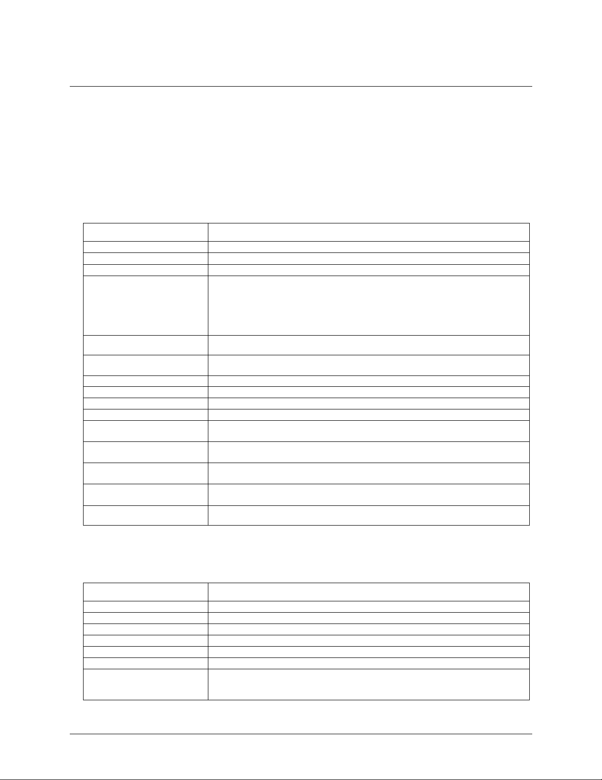
Digital input/ output
Table 1. Dig it al I/ O spec if icat ions
Para m e t er
Spe cif icat ion
Digital type
TTL
Number of I/O
32 (2 ports of 16 bits)
Configuration
Bit-configurable as input (power on default) or output
Pull-up configuration
Each port has two 47 kΩ resistors configurable as a pull-up or pull-down (default) with
an internal jumper. Each jumper configures 8 digital bits.
■ Jumper W3 configures port 0 bit 0 to bit 7
■ Jumper W4 configures port 0 bit 8 to bit 15
■ Jumper W5 configures port 1 bit 0 to bit 7
■ Jumper W6 configures port 1 bit 8 to bit 15
Digital I/O transfer rate
(system-paced, asynchronous)
33 to 8000 port reads/writes or single bit reads/writes per second typical,
system dependent.
Digital I/O transfer rate
(synchronous)
0.022 Hz to 8 MHz, based on the internal clock speed of 96 MHz
Digital input pacing
Onboard clock, external input scan clock (ICLKI)
Digital input trigger source
External single channel digital trigger (TRIG) or Pattern Detection
Digital output pacing
Onboard clock, external output scan clock (OCLKI)
Digital output trigger source
External single channel digital trigger (TRIG) or Pattern Detection
Input high voltage
2.0 V min
5.0 V absolute max
Input low voltage
0.8 V max
0 V recommended min
Output high voltage
4.4 V min (IOH = –50 µA)
2.96 V min (IOH = –24 mA)
Output low voltage
0.1 V max (IOL = 50 µA)
0.77 V max (IOL = 10 mA)
Output current
24 mA source, 10 mA sink max per pin, constrained to 384 mA across all output pins
(digital outputs, pacer clock outputs, and +VO)
Ext e rnal t rig ge r
Table 2. Digit al t rigger specif icat ions
Para m e t er
Spe cif icat ion
Trigger source
External digital; TRIG terminal
Trigger mode
Software-selectable for edge or level sensitive, rising or falling edge, high or low level.
Retrigger mode
Trigger is rearmed after each trigger event
Trigger latency
100 ns max
Trigger pulse width
100 ns min
Input type
Schmitt trigger, 47 kΩ pull-down to ground with 33 Ω in series
Schmitt trigger hysteresis
0.76 V typ
0.4 V min
1.2 V max
Page 14
OM-USB-32DIO User's Guide Specifications
14
Preliminary
Para m e t er
Spe cif icat ion
Input high voltage threshold
1.74 V typ
1.3 V min
2.2 V max
Input high voltage limit
5.5 V absolute max
Input low voltage threshold
0.98 V typ
0.6 V min
1.5 V max
Input low voltage limit
–0.5 V absolute min
0 V recommended min
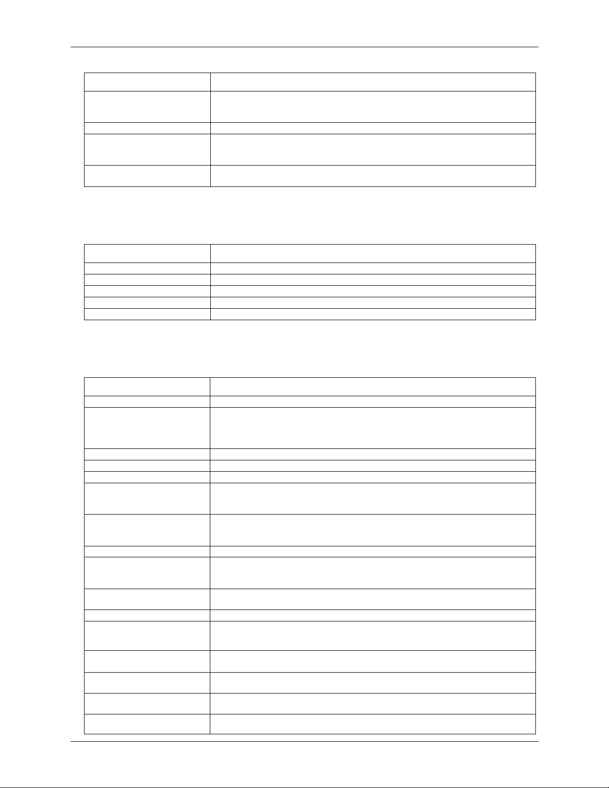
Pat t ern trigger
Table 3. Pat t ern t rigger specif icat ions
Para m e t er
Spe cif icat ion
Trigger source
Port 0 or Port 1
Trigger types
Above pattern, Below pattern, Equal pattern, or Not equal pattern
Trigger stability
Digital port must be stable for 31.25 ns to be recognized as a pattern
Trigger bit width
Up to 16, adjustable through bitmask
Trigger latency
Up to 1 scan period
Clock input /output
Table 4. Clock I/ O specif icat ions
Para m e t er
Spe cif icat ion
Terminal names
ICLKI, ICLKO, OCLKI, OCLKO
Terminal type
ICLKI: Input scan clock input, active on rising edge
ICLKO: Input scan clock output, power on default is 0V, active on rising edge
OCLKI: Output scan clock input, active on rising edge
OCLKO: Output scan clock output, power on default is 0V, active on rising edge
Input clock frequency
8 MHz, max
Input clock pulse width
10.417 ns min
Input type
Schmitt trigger, 47 kΩ pull-down to ground with 33 Ω in series
Input Schmitt trigger hysteresis
0.76 V typ
0.4 V min
1.2 V max
Input high voltage threshold
1.74 V typ
1.3 V min
2.2 V max
Input high voltage limit
5.5 V absolute max
Input low voltage threshold
0.98 V typ
0.6 V min
1.5 V max
Input low voltage limit
–0.5 V absolute min
0 V recommended min
Output clock frequency
8 MHz, max
Output clock pulse width
Minimum 62.5 ns at 8 MHz, but varies according to the sample rate; always maintains
a 50% duty cycle when using the internal clock. When using the external clock, it
follows the external clock input.
Output high voltage
4.4 V min (IOH = –50 µA)
2.96 V min (IOH = –24 mA)
Output low voltage
0.1 V max (IOL = 50 µA)
0.77 V max (IOL = 10 mA)
Output current
24 mA source, 10mA sink max per pin, constrained to 384 mA across all output pins
(digital outputs, pacer clock outputs, and +VO)
Handshaking
The TXACK output will have an 83.33ns delay from the OCLKO signal to ensure
coherent data transfers between devices.
Page 15
OM-USB-32DIO User's Guide Specifications
15
Preliminary
Memory
Table 5. Memory specifications
Para m e t er
Spe cif icat ion
FIFO
8 KS
Non-volatile EEPROM
32 KB (10 KB firmware storage, 22 KB user data)
Powe r
Table 6. Power specificat ions
Para m e t er
Condit ion
Spe cif icat ion
Supply current, USB source
During enumeration
< 100 mA
After USB enumeration
< 500 mA
+VO voltage output range
After USB enumeration
5 V, ± 5%
+VO output current
After USB enumeration
24 mA max per pin, constrained to 384 mA across all
output pins (digital outputs, pacer clock outputs, and +VO)
USB
Table 7. USB specifications
Para m e t er
Spe cif icat ion
USB device type
USB 2.0 (high-speed)
Device compatibility
USB 1.1, USB 2.0, USB 3.0
USB cable type
A-B cable, UL type AWM 2725 or equivalent. Min 24 AWG VBUS/GND,
min 28 AWG D+/D–.
USB cable length
3 m (9.84 ft) max
Envir onment al
Table 8. Environment al specificat ions
Para m e t er
Spe cif icat ion
Operating temperature range
0 °C to 50 °C
Storage temperature range
–40 °C to 70 °C
Humidity
0% to 90% non-condensing
Mechanical
Table 9. Mechanical specifications
Para m e t er
Spe cif icat ion
Dimensions (L × W × H)
128.52 × 88.39 × 35.56 mm (5.06 × 3.48 × 1.43 in.)
Signal conne ct or
Table 10. Scr ew terminal specif icat ions
Para m e t er
Spe cif icat ion
Connector type
Screw terminal
Wire gauge range
16 AWG to 30 AWG
Page 16

OM-USB-32DIO User's Guide Specifications
16
Preliminary
Screw t erminal pinout
Table 11. Screw t erminal pinout
Pin
Signal name
Pin descript ion
Pin
Signal name
Pin descript ion
1
P0 D0
Po rt 0 bi t 0
29
P1 D0
Po rt 1 bi t 0
2
P0 D1
Po rt 0 bi t 1
30
P1 D1
Po rt 1 bi t 1
3
GND
Digit al g rou nd
31
GND
Digit al g rou nd
4
P0 D2
Po rt 0 bi t 2
32
P1 D2
Po rt 1 bi t 2
5
P0 D3
Po rt 0 bi t 3
33
P1 D3
Po rt 1 bi t 3
6
GND
Digit al g rou nd
34
GND
Digit al g rou nd
7
P0 D4
Po rt 0 bi t 4
35
P1 D4
Po rt 1 bi t 4
8
P0 D5
Po rt 0 bi t 5
36
P1 D5
Po rt 1 bi t 5
9
GND
Digit al g rou nd
37
GND
Digit al g rou nd
10
P0 D6
Po rt 0 bi t 6
38
P1 D6
Po rt 1 bi t 6
11
P0 D7
Po rt 0 bi t 7
39
P1 D7
Po rt 1 bi t 7
12
GND
Digit al g rou nd
40
GND
Digit al g rou nd
13
P0 D8
Po rt 0 bi t 8
41
P1 D8
Po rt 1 bi t 8
14
P0 D9
Po rt 0 bi t 9
42
P1 D9
Po rt 1 bi t 9
15
GND
Digit al g rou nd
43
GND
Digit al g rou nd
16
P0 D1 0
Po rt 0 bi t 1 0
44
P1 D1 0
Po rt 1 bi t 1 0
17
P0 D1 1
Po rt 0 bi t 1 1
45
P1 D1 1
Po rt 1 bi t 1 1
18
GND
Digit al g rou nd
46
GND
Digit al g rou nd
19
P0 D1 2
Po rt 0 bi t 1 2
47
P1 D1 2
Po rt 1 bi t 1 2
20
P0 D1 3
Po rt 0 bi t 1 3
48
P1 D1 3
Po rt 1 bi t 1 3
21
GND
Digit al g rou nd
49
GND
Digit al g rou nd
22
P0 D1 4
Po rt 0 bi t 1 4
50
P1 D1 4
Po rt 1 bi t 1 4
23
P0 D1 5
Po rt 0 bi t 1 5
51
P1 D1 5
Po rt 1 bi t 1 5
24
GND
Digit al g rou nd
52
GND
Digit al g rou nd
25
ICLKI
Inp u t s can cl ock inp u t
53
ICLKO
Inp u t s can cl ock o ut pu t
26
OCLKI
Out p ut scan c loc k input
54
OCLKO
Out p ut scan c loc k output
27
TRIG
Ex t er na l t r i gg e r in pu t
55
+VO
Use r v olt ag e out pu t
28
RSV D
Re se r v e d f o r f u t u r e u se
56
TXACK
Dat a t ransfer out put
Page 17

WARRANTY/DISCLAIMER
OMEGA ENGINEERING, INC. warrants this unit to be free of defects in materials and workmanship for a
period of 13 months from date of purchase. OMEGA’s WARRANTY adds an additional one (1) month grace
period to the normal one (1) year product warranty to cover handling and shipping time. This ensures
that OMEGA’s customers receive maximum coverage on each product.
If the unit malfunctions, it must be returned to the factory for evaluation. OMEGA’s Customer Service
Department will issue an Authorized Return (AR) number immediately upon phone or written request.
Upon examination by OMEGA, if the unit is found to be defective, it will be repaired or replaced at no
charge. OMEGA’s WARRANTY does not apply to defects resulting from any action of the purchaser,
including but not limited to mishandling, improper interfacing, operation outside of design limits,
improper repair, or unauthorized modification. This WARRANTY is VOID if the unit shows evidence of
having been tampered with or shows evidence of having been damaged as a result of excessive corrosion;
or current, heat, moisture or vibration; improper specification; misapplication; misuse or other operating
conditions outside of OMEGA’s control. Components in which wear is not warranted, include but are not
limited to contact points, fuses, and triacs.
OMEGA is pleased to offer suggestions on the use of its various products. However,
OMEGA neither assumes responsibility for any omissions or errors nor assumes liability for
any damages that result from the use of its products in accordance with information provided
by OMEGA, either verbal or written. OMEGA warrants only that the parts manufactured by the
company will be as specified and free of defects. OMEGA MAKES NO OTHER WARRANTIES OR
REPRESENTATIONS OF ANY KIND WHATSOEVER, EXPRESSED OR IMPLIED, EXCEPT THAT OF
TITLE, AND ALL IMPLIED WARRANTIES INCLUDING ANY WARRANTY OF MERCHANTABILITY
AND FITNESS FOR A PARTICULAR PURPOSE ARE HEREBY DISCLAIMED. LIMITATION OF
LIABILITY: The remedies of purchaser set forth herein are exclusive, and the total liability of
OMEGA with respect to this order, whether based on contract, warranty, negligence,
indemnification, strict liability or otherwise, shall not exceed the purchase price of the
component upon which liability is based. In no event shall OMEGA be liable for
consequential, incidental or special damages.
CONDITIONS: Equipment sold by OMEGA is not intended to be used, nor shall it be used: (1) as a “Basic
Component” under 10 CFR 21 (NRC), used in or with any nuclear installation or activity; or (2) in medical
applications or used on humans. Should any Product(s) be used in or with any nuclear installation or
activity, medical application, used on humans, or misused in any way, OMEGA assumes no responsibility
as set forth in our basic WARRANTY/DISCLAIMER language, and, additionally, purchaser will indemnify
OMEGA and hold OMEGA harmless from any liability or damage whatsoever arising out of the use of the
Product(s) in such a manner.
RETURN REQUESTS/INQUIRIES
Direct all warranty and repair requests/inquiries to the OMEGA Customer Service Department. BEFORE
RETURNING ANY PRODUCT(S) TO OMEGA, PURCHASER MUST OBTAIN AN AUTHORIZED RETURN (AR)
NUMBER FROM OMEGA’S CUSTOMER SERVICE DEPARTMENT (IN ORDER TO AVOID PROCESSING
DELAYS). The assigned AR number should then be marked on the outside of the return package and on any
correspondence.
The purchaser is responsible for shipping charges, freight, insurance and proper packaging to prevent
breakage in transit.
FOR WARRANTY RETURNS, please have the
following information available BEFORE contacting
OMEGA:
1. Purchase Order number under which the product
was PURCHASED,
2. Model and serial number of the product under
warranty, and
3. Repair instructions and/or specific problems
relative to the product.
OMEGA’s policy is to make running changes, not model changes, whenever an improvement is possible. This affords our
customers the latest in technology and engineering.
OMEGA is a registered trademark of OMEGA ENGINEERING, INC.
© Copyright 2016 OMEGA ENGINEERING, INC. All rights reserved. This document may not be copied, photocopied,
reproduced, translated, or reduced to any electronic medium or machine-readable form, in whole or in part, without the prior
written consent of OMEGA ENGINEERING, INC.
FOR NON-WARRANTY REPAIRS, consult
OMEGA for current repair charges. Have
the following information available BEFORE
contacting OMEGA:
1. Purchase Order number to cover the COST
of the repair,
2. Model and serial number of the product, and
3. Repair instructions and/or specific problems
relative to the product.
Page 18

Where Do I Find Everything I Need for
Process Measurement and Control?
OMEGA…Of Course!
Shop online at omega.com
TEMPERATURE
MU
Thermocouple, RTD & Thermistor Probes, Connectors,
Panels & Assemblies
MU
Wire: Thermocouple, RTD & Thermistor
MU
Calibrators & Ice Point References
MU
Recorders, Controllers & Process Monitors
MU
Infrared Pyrometers
PRESSURE, STRAIN AND FORCE
MU
Transducers & Strain Gages
MU
Load Cells & Pressure Gages
MU
Displacement Transducers
MU
Instrumentation & Accessories
FLOW/LEVEL
MU
Rotameters, Gas Mass Flowmeters & Flow Computers
MU
Air Velocity Indicators
MU
Turbine/Paddlewheel Systems
MU
Totalizers & Batch Controllers
SM
pH/CONDUCTIVITY
MU
pH Electrodes, Testers & Accessories
MU
Benchtop/Laboratory Meters
MU
Controllers, Calibrators, Simulators & Pumps
MU
Industrial pH & Conductivity Equipment
DATA ACQUISITION
MU
Data Acquisition & Engineering Software
MU
Communications-Based Acquisition Systems
MU
Plug-in Cards for Apple, IBM & Compatibles
MU
Data Logging Systems
MU
Recorders, Printers & Plotters
HEATERS
MU
Heating Cable
MU
Cartridge & Strip Heaters
MU
Immersion & Band Heaters
MU
Flexible Heaters
MU
Laboratory Heaters
ENVIRONMENTAL
MONITORING AND CONTROL
MU
Metering & Control Instrumentation
MU
Refractometers
MU
Pumps & Tubing
MU
Air, Soil & Water Monitors
MU
Industrial Water & Wastewater Treatment
MU
pH, Conductivity & Dissolved Oxygen Instruments
M5555/0216
 Loading...