

Page 1

Contents
INTRODUCTION.....................................................................1
OVERVIEW..................................................................................1
WHAT’S INCLUDED .....................................................................1
FACTORY DEFAULT SETTINGS .....................................................1
CARD SETUP .........................................................................2
ADDRESS SELECTION ..................................................................2
IRQ SELECTION (HEADER E8)..................................................... 3
DMA OPTIONS........................................................................... 4
Header E3...............................................................................4
Header E5...............................................................................5
Commonly Used DMA Jumper Options...................................6
HEADERS E1 AND E2 ..................................................................7
RS-485 ENABLE .........................................................................8
INSTALLATION......................................................................9
CABLING OPTIONS ......................................................................9
TECHNICAL DESCRIPTION..................................................10
FEATURES.................................................................................10
Internal Baud Rate Generator................................................10
PROGRAMMING THE OMG-ACB-IV..........................................11
Control/Status Port ................................................................ 11
Software Examples................................................................ 11
CONNECTOR P1 AND P2 PIN ASSIGNMENTS................................12
RS-530/422/485 Line Termination........................................12
SPECIFICATIONS .................................................................13
ENVIRONMENTAL SPECIFICATIONS............................................. 13
POWER CONSUMPTION ..............................................................13
MEAN TIME BETWEEN FAILURES (MTBF).................................. 13
PHYSICAL DIMENSIONS ............................................................. 13
APPENDIX A - TROUBLESHOOTING ....................................14
APPENDIX B - HOW TO GET ASSISTANCE..........................15
APPENDIX C - ELECTRICAL INTERFACE ............................16
RS-422.....................................................................................16
RS-530.....................................................................................16
RS-449.....................................................................................16
RS-485.....................................................................................17
APPENDIX D - DIRECT MEMORY ACCESS ..........................18
Page 2

APPENDIX E - ASYNCHRONOUS AND SYNCHRONOUS
COMMUNICATIONS ............................................................. 19
ASYNCHRONOUS COMMUNICATIONS..........................................19
SYNCHRONOUS COMMUNICATIONS ............................................21
APPENDIX F - ACB DEVELOPER TOOLKIT DISKETTE AND
ACB RESOURCE KIT.......................................................... 23
APPENDIX G - SILK-SCREEN ..............................................24
APPENDIX H - COMPLIANCE NOTICES............................... 25
FEDERAL COMMUNICATIONS COMMISSION STATEMENT..............25
EMC DIRECTIVE STATEMENT....................................................25
WARRANTY......................................................................... 26
Figures
Figure 1 - Address Selection Table........................................................2
Figure 2 - DIP-switch Illustration..........................................................2
Figure 3 - Header E8, IRQ Selection ....................................................3
Figure 4 - Header E3 .............................................................................4
Figure 5 - Header E5 .............................................................................5
Figure 6 - Commonly Used DMA Options ............................................6
Figure 7 - Headers E1 and E2 Clock Input/Output Modes ..................7
Figure 8 - Control/Status Register Bit Definitions..............................11
Figure 9 - Control/Status Register Examples......................................11
Figure 10 - Asynchronous Communications Bit Diagram...................20
Figure 11 - Synchronous Communications Bit Diagram.....................21
© 1996h Omega Engineering, Incorporated. All rights reserved.
Page 3

Introduction
Introduction
Overview
The Omega Engineering OMG-ACB-IV provides the PC with two high
speed RS-530/422/485 sync/async ports. The OMG-ACB-IV can be used
in a variety of sophisticated communications applications such as SDLC,
HDLC, X.25, and high speed async.
What’s Included
The OMG-ACB-IV is shipped with the following items. If any of these
items are missing or damaged, contact the supplier.
• OMG-ACB-IV Serial Interface Adapter
• 3.5″ ACB Developers Toolkit Diskette
• Channel B Interface Cable
• User Manual
Factory Default Settings
The OMG-ACB-IV factory default settings are as follows:
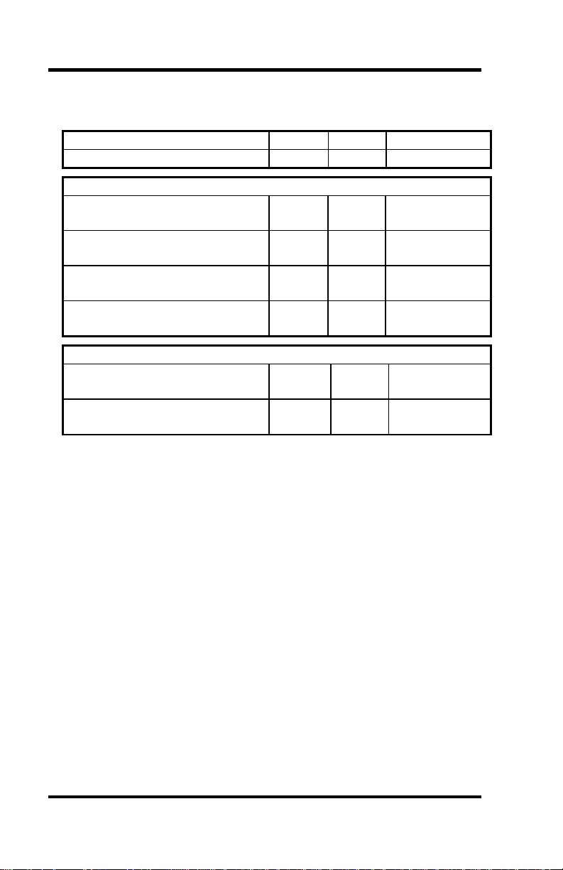
Base Address DMA Channels IRQ Electrical Specification
238 TX: 1/RX: 3 5 RS-530/422
To install the OMG-ACB-IV using factory default settings, refer to the
section on Installation.
For your reference, record installed OMG-ACB-IV settings below:
Base Address DMA Channel IRQ Electrical Specification
Omega Engineering OMG-ACB-IV Page 1
Page 4
Card Setup
Card Setup
The OMG-ACB-IV contains several jumper straps for each port which
must be set for proper operation.
Address Selection
The OMG-ACB-IV occupies 8 consecutive I/O locations. A DIP-switch
(SW1) is used to set the base address for these locations. The OMG-
ACB-IV can reside in any I/O location between 100 and 3F8 Hex. Be
careful when selecting the base address as some selections conflict with
existing PC ports. The following table shows several examples that
usually do not cause a conflict.
Address Binary Switch Settings
A9----------A0 1 2 3 4 5 6 7
238-23F 1000111XXX Off On On On Off Off Off
280-287 1010000XXX Off On Off On On On On
2A0-2A7 1010100XXX Off On Off On Off On On
2E8-2EF 1011101XXX Off On Off Off Off On Off
300-307 1100000XXX Off Off On On On On On
328-32F 1100101XXX Off Off On On Off On Off
3E8-3EF 1111101XXX Off Off Off Off Off On Off
Figure 1 - Address Selection Table
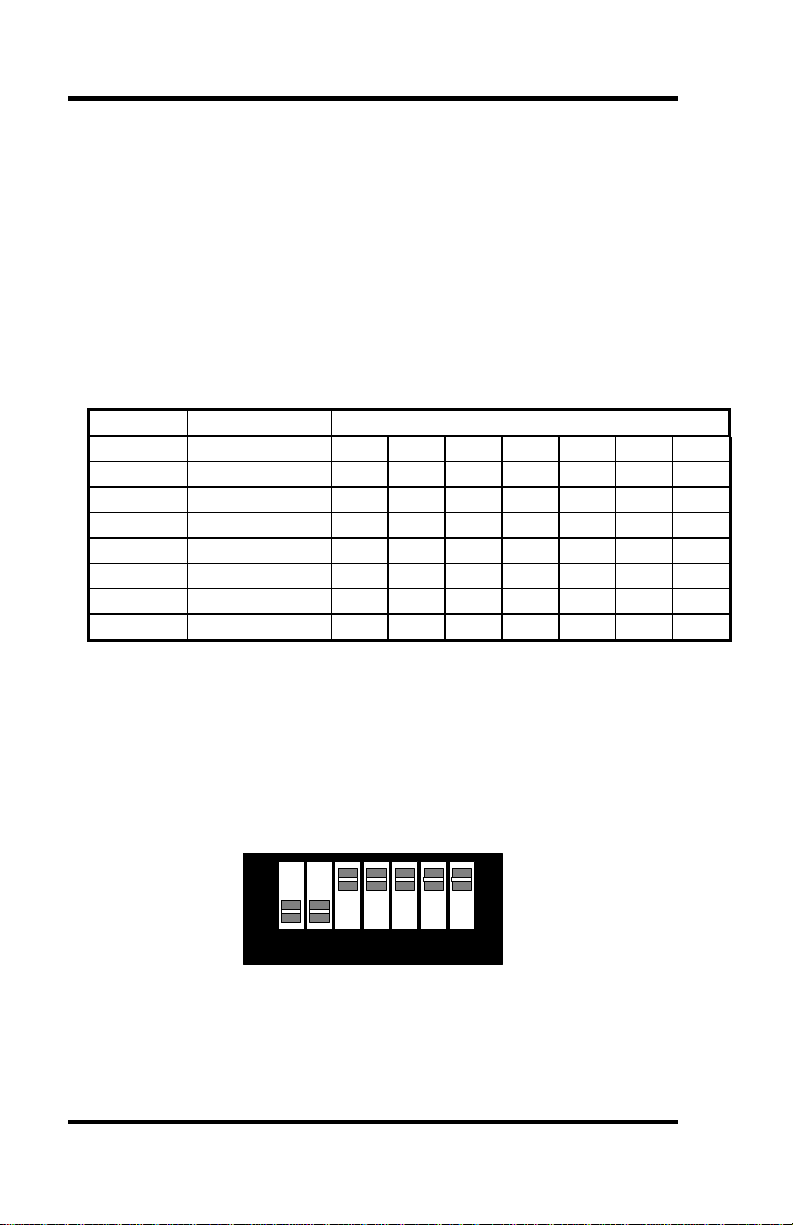
The following illustration shows the correlation between the DIP-switch
setting and the address bits used to determine the base address. In the
example below, the address 300 Hex through 307 Hex is selected.
300 Hex = 11 0000 0XXX in binary representation.
A9
ON
OFF
A3
1 2 3 4 5 6 7
Figure 2 - DIP-switch Illustration
Note: Setting the switch ‘On’ or ‘Closed’ corresponds to a ‘0’ in the
address, while leaving it ‘Off’ or ‘Open’ corresponds to a ‘1’.
Omega Engineering OMG-ACB-IV Page 2
Page 5
Card Setup
The relative I/O address of the 8530 SCC registers is as follows:
Base+0 Channel A Data Port
Base+1 Channel A Control Port
Base+2 Channel B Data Port
Base+3 Channel B Control Port
(Base+4) Board Control/Status Port
Where ‘Base’ is the selected board base address.
IRQ Selection (Header E8)
The OMG-ACB-IV has an interrupt selection jumper which should be set
prior to use, if an interrupt is required by your application software.
Consult the user manual for the application software being used to
determine the proper setting.
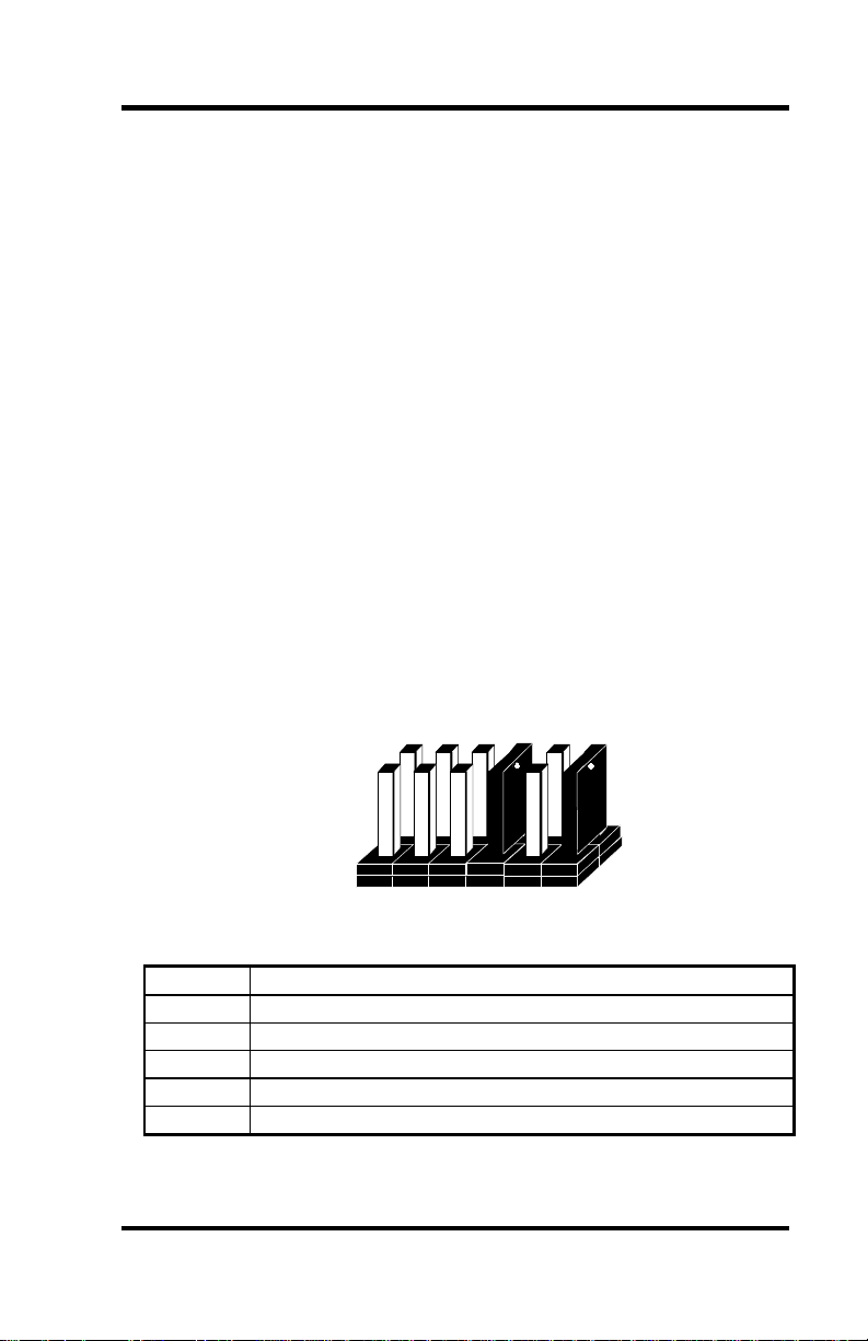
Positions ‘M’ & ‘N’ allow the user to select a single interrupt per port
mode or a shared interrupt mode. The ‘N’ selects the single interrupt per
port mode. The ‘M’ selects the shared interrupt mode, which allows more
than one port to access a single IRQ, and indicates the inclusion of a 1K
ohm pull-down resistor required on one port when sharing interrupts.
The diagram below shows IRQ 5 selected in a shared configuration. If no
interrupt is desired, remove both jumpers.
2 3 4 5E8NM
2/9 Selects IRQ2/9
3 Selects IRQ3
4 Selects IRQ4
5 Selects IRQ5
N Selects Normal IRQ Mode
M Selects ‘Multi-IRQ’ (Shared) IRQ Mode
Figure 3 - Header E8, IRQ Selection
Omega Engineering OMG-ACB-IV Page 3
Page 6
Card Setup
12345
6
DMA Options
Headers E3 and E5 select the Direct Memory Access (DMA) mode of
operation for the OMG-ACB-IV. Channel A of the SCC can operate in
either half-duplex or full duplex DMA mode. Full duplex DMA can
transmit and receive data simultaneously. Half-duplex DMA can transmit
or receive data, but not in both directions simultaneously. Refer to Page 6
for the most common DMA settings.
Note: If DMA is not used, remove all of the jumpers on E3 and E5.
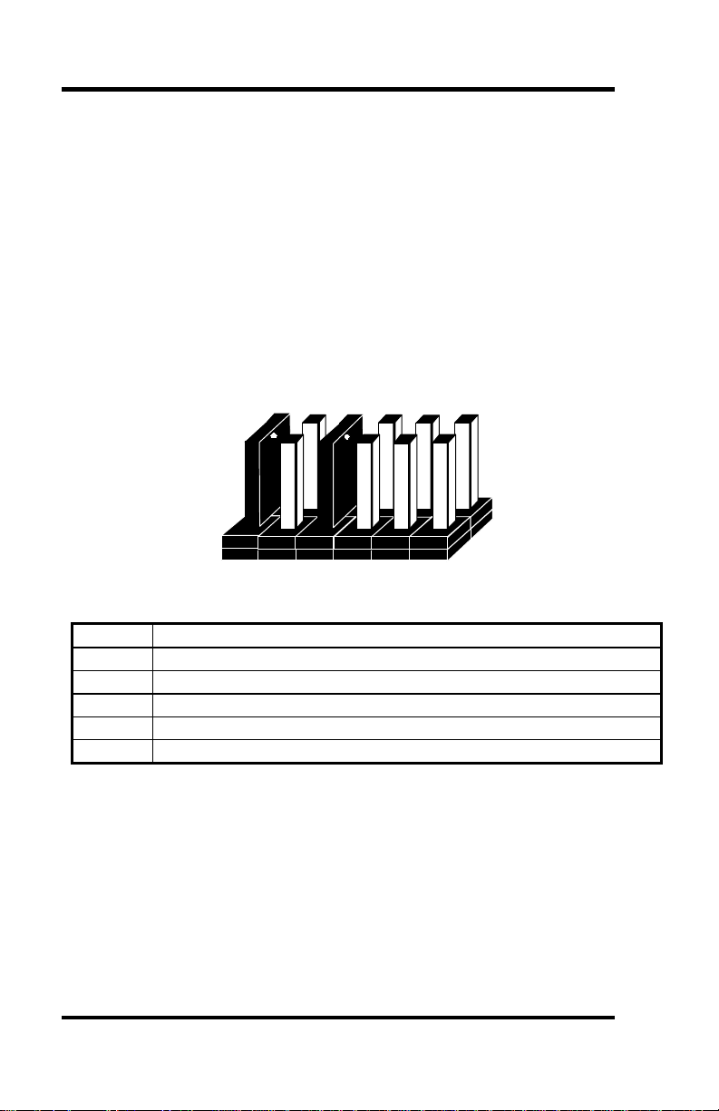
Header E3
1 DACK 1 Or 3 Acknowledge For Two Channel Mode
2 Two Channel A/B Mode A3B1
3 Two Channel A/B Mode A1B3
4 On = Ch. A Only / Off = Ch. B Only
5 DACK 3 DMA Acknowledge Channel 3
6 DACK 1 DMA Acknowledge Channel 1
Figure 4 - Header E3
Omega Engineering OMG-ACB-IV Page 4
Page 7
Card Setup
1234567
8
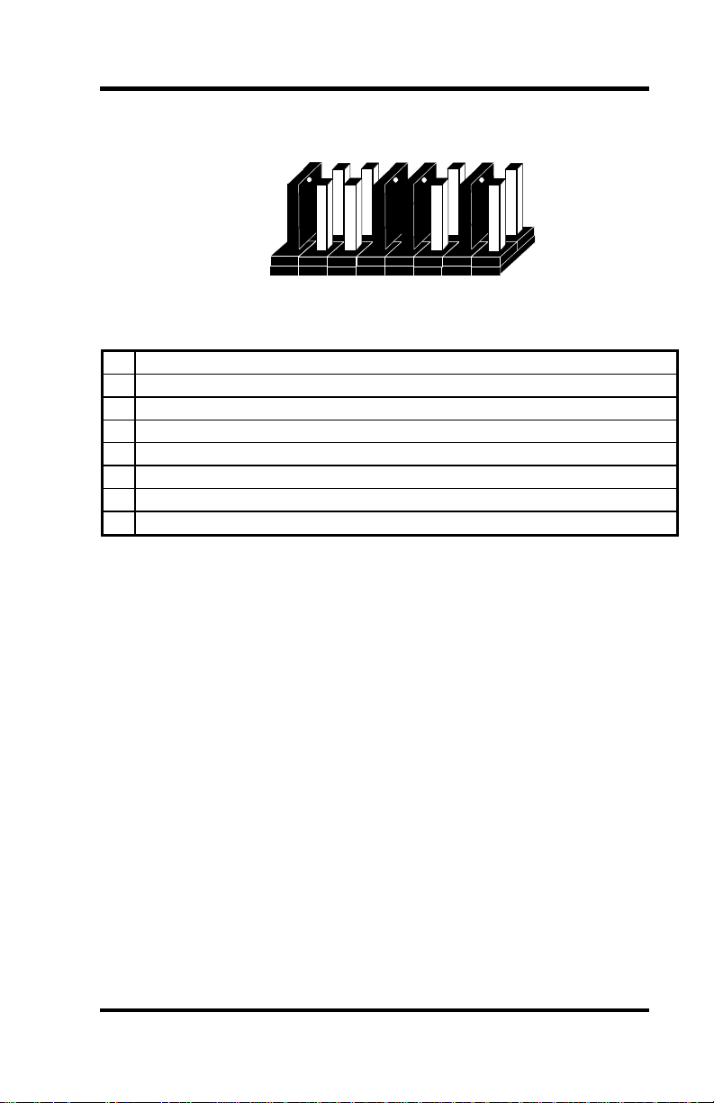
Header E5
1 SCC Channel A or B can use DMA Channel 3
2 SCC Channel A only can use DMA Channel 3
3 SCC Channel A or B can use DMA Channel 1
4 SCC Channel A only can use DMA Channel 1
5 SCC Channel B Enable for Half Duplex DMA Transfers
6 SCC Channel A, DMA Channel 1 & 3 for Full Duplex Transfers
7 DMA Tri-State drivers permanently enabled
8 DMA Tri-State drivers enabled by status / control port bit 7
Figure 5 - Header E5
Positions 7 and 8 of Header E5 enable or disable DMA operation. A
jumper ‘ON’ position 7 permanently enables the DMA tri-state drivers. A
jumper ‘ON’ position 8 places DMA under software control via the DMA
enable control port bit (located at Base+4). Removing the jumper disables
the drivers, and no DMA can be performed.
Note: The power-on reset signal disables the DMA enable signal. A
jumper placed in position 7 of E5 will override any software use of
the DMA enable/disable status port bit.
Omega Engineering OMG-ACB-IV Page 5
Page 8
Commonly Used DMA Jumper Options
Option E3 E5 Program 8530
No DMA
Single Channel DMA (Half-Duplex Only):
Ch. A DMA Ch.1 Half Duplex
Ch. B No DMA
Ch. A DMA Ch.1 Half Duplex
Ch. B No DMA
Ch. B DMA Ch.1 Half Duplex
Ch. B No DMA
Ch. B DMA Ch.1 Half Duplex
Ch. A No DMA
Full Duplex using Both DMA Channels 1 and 3:
Ch.A DMA Ch.1 Receive Data
Ch.A DMA Ch.3 Transmit Data
Ch.A DMA Ch.3 Receive Data
Ch.A DMA Ch.1 Transmit Data
Figure 6 - Commonly Used DMA Options
None None N/A
4,6 4,5 WAIT/REQ A
4,5 2,5 WAIT/REQ A
6 3,5 WAIT/REQ B
5 1,5 WAIT/REQ B
1,4 1,4,6 WAIT/REQ A
1,4 2,3,6 WAIT/REQ A
Card Setup
DTR/REQ A
DTR/REQ A
Remember that E5 positions 7 and 8 enable or disable DMA
operation.
Omega Engineering OMG-ACB-IV Page 6
Page 9
Card Setup
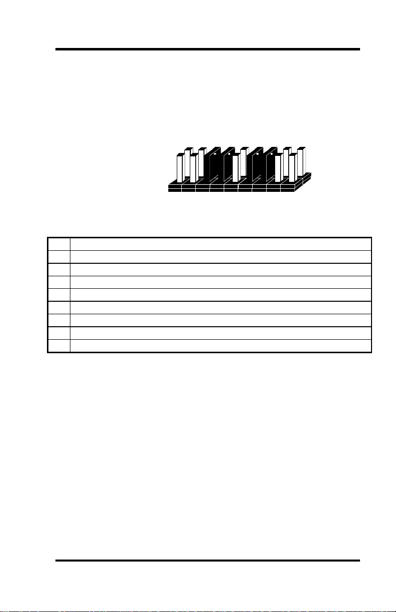
Headers E1 and E2
Headers E1 and E2 set the input/output clock modes for the transmit clock
(TXC), as well as the RS-485 enable/disable. E1 sets the clock mode for
the SCC Channel B (Port 2), while E2 sets the clock mode for the SCC
channel A (Port 1).
TX
RX TX
RX
E1
Silkscreen
Table
1 Enable (for RS-485 mode only)
2 Transmit Clock Input (TXC In on pins 12 and 15 of the DB-25)
3* Transmit Clock Output (TXC Out on pins 12 and 15 of the DB-25)
4* Receive Clock Input (RXC In on pins 17 and 9)**
5 Not Used (Leave Jumper Off)
6* Transmit Clock Output (TXC Out on pins 12 and 15 of the DB-25)
7* Transmit Clock Output (TXC Out on pins 12 and 15 of the DB-25)
8 Not Used (Leave Jumper Off)**
9 Not Used (Leave Jumper Off)**
Figure 7 - Headers E1 and E2 Clock Input/Output Modes
*Factory default
**These jumpers are always configured in this manner and should not be
removed or replaced.
I O I O O O OE O
1 2 3 4 5 6 7 8 9
Note: The TXC pins (12 and 15) can be programmed as either an input or
an output. The TSET pins (11 and 24) will always echo the TXC
pins, regardless of whether the TXC pins are selected as an input or
an output.
Omega Engineering OMG-ACB-IV Page 7
Page 10

Card Setup
RS-485 Enable
To enable the driver in RS-485 mode, place a jumper over position 1 on
E1 for port 2 and position 1 on E2 for port 1, then assert RTS
(Write Register 5 position D1=1) to transmit and de-assert RTS
(Write Register 5 position D1=0) when finished transmitting. To
permanently enable the driver (normal EIA-530/RS-422 point to point
mode), remove jumper at position 1 on E1 and E2. Half-duplex two-wire
operation is also possible by connecting TX+ to RX+ and TX- to RX- in
the cable hood. The unused EIA-530 signals can be left disconnected or
floating, as they have pull-up/pull-down resistors to provide an ‘On’
condition, if not connected.
Omega Engineering OMG-ACB-IV Page 8
Page 11

Installation
Installation
The OMG-ACB-IV can be installed in any of the PC expansion. The
OMG-ACB-IV contains several jumper straps for each port which must
be set for proper operation.
1. Turn off PC power. Disconnect the power cord.
2. Remove the PC case cover.
3. Locate two available slots and remove the blank metal slot covers.
4. Install the Channel B cable into Box Header E4. This cable is keyed
to prevent improper installation. Gently insert the OMG-ACB-IV
into the slot. Make sure that the adapter is seated properly. Attach the
Channel B cable to the adjacent slot with the retaining screw. (If
Channel B of the OMG-ACB-IV is not used, the adapter cable is not
required).
5. Replace the cover.
6. Connect the power cord.
Installation is complete.
Cabling Options
The OMG-ACB-IV has a number of cabling options available. These
options include:
• CA-104 - This cable provides a 6′ extension for use with RS-530/422
• CA-107 - This cable provides a simple interface to the older RS-449,
DB-37 type connector. RS-530 was designed as a replacement for
RS-449.
Omega Engineering OMG-ACB-IV Page 9
Page 12

Technical Description
Technical Description
The OMG-ACB-IV utilizes the Zilog 8530 Serial Communications
Controller (SCC). This chip features programmable baud rate, data format
and interrupt control, as well as DMA control. Refer to the SCC Users
Manual for details on programming the SCC 8530 chip.
Features
• Two channels of sync/async communications using 8530 chip
• DMA supports data rate greater than 1 million bps (bits per second)
• Select-able Port Address, IRQ level (2/9,3,4,5), and DMA channel
(1 or 3)
• EIA-530/422 interface with full modem control supports TD, RD,
RTS, CTS, DSR, DCD, DTR, TXC, RXC, LL, RL, TM signals
• Jumper options for clock source
• Software programmable baud rate
• High Speed Enhanced Serial Communications Controller
(85C30,85230) compatible
Internal Baud Rate Generator
The baud rate of the SCC is programmed under software control. The
standard oscillator supplied with the board is 7.3728 MHz. However,
other oscillator values can be substituted to achieve different baud rates.
Omega Engineering OMG-ACB-IV Page 10
Page 13
Technical Description
Programming The OMG-ACB-IV
Control/Status Port
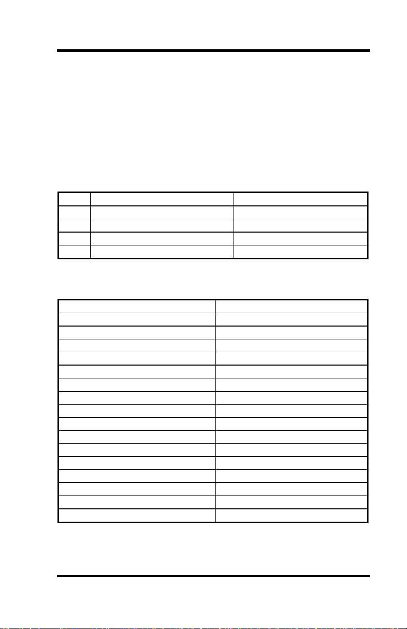
The OMG-ACB-IV occupies eight Input/Output (I/O) addresses. The
first four are used by the SCC chip, while the fifth address (Base+4) is the
address of the on-board Control/Status Port. This port is used to set the
Data Terminal Ready (DTR) signal, to enable or disable DMA under
program control, and to monitor the Data Set Ready (DSR) input signals
from the modem. The following table lists bit positions of the
Control/Status port.
Bit Output Port Bits Input Port Bits
0 DTR A 1=On, 0=Off DSR A 1=On, 0=Off
1 DTR B 1=On, 0=Off DSR B 1=On, 0=Off
2-6 Not Used Not Used
7 DMA Enable 1=On, 0=Off Not Used
Figure 8 - Control/Status Register Bit Definitions
Software Examples
Function Program Bits
Turn On CH. A DTR Out (Base+4),XXXX XXX1
Turn On CH. B DTR Out (Base+4),XXXX XX1X
Turn Off CH. A DTR Out (Base+4),XXXX XXX0
Turn Off CH. B DTR Out (Base+4),XXXX XX0X
Turn On CH. A LL Out (Base+4),XXXX X1XX
Turn On CH. B LL Out (Base+4),XXX1 XXXX
Turn On CH. A RL Out (Base+4),XXXX 1XXX
Turn On CH. B RL Out (Base+4),XX1X XXXX
Turn Off CH. A LL Out (Base+4),XXXX X0XX
Turn Off CH. B RL Out (Base+4),XX0X XXXX
Enable DMA Drivers Out (Base+4),1XXX XXXX
Disable DMA Drivers Out (Base+4),0XXX XXXX
Test CH. A DSR In (Base+4), Mask=0000 0001
Test CH. B DSR In (Base+4), Mask=0000 0010
Test CH. A TM In (Base+4), Mask=0000 0100
Test CH. B TM In (Base+4), Mask=0001 0000
Figure 9 - Control/Status Register Examples
Omega Engineering OMG-ACB-IV Page 11
Page 14
Technical Description
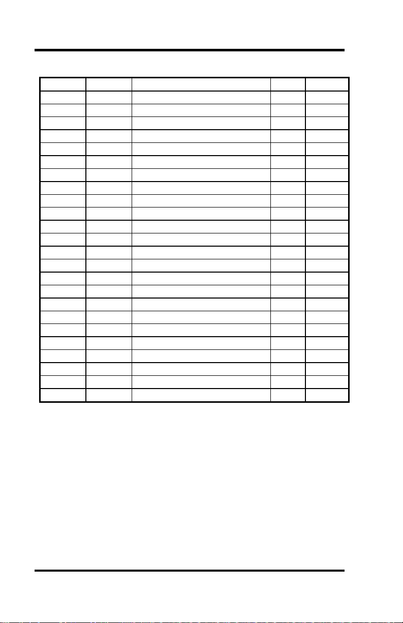
Connector P1 and P2 Pin Assignments
Signal Name Pin # Mode
GND Ground 7
RDB RX+ Receive Positive 16 Input
RDA RX- Receive Negative 3 Input
CTSB CTS+ Clear To Send Positive 13 Input
CTSA CTS- Clear To Send Negative 5 Input
DSRB DSR+ Data Set Ready Positive 22 Input
DSRA DSR- Data Set Ready Negative 6 Input
DCDB DCD+ Data Carrier Detect Positive 10 Input
DCDA DCD Data Carrier Detect Negative 8 Input
TDB TX+ Transmit Positive 14 Output
TDA TX- Transmit Negative 2 Output
RTSB RTS+ Request To Send Positive 19 Output
RTSA RTS- Request To Send Negative 4 Output
DTRB DTR+ Data Terminal. Ready Positive 23 Output
DTRA DTR- Data Terminal Ready Negative 20 Output
TXCB TXC+ Transmit Clock Positive 12 Input
TXCA TXC- Transmit Clock Negative 15 Input
RXCB RXC+ Receive Clock Positive 9 Input
RXCA RXC- Receive Clock Negative 17 Input
TSETB TSET+ Terminal Timing Positive 11 Output
TSETA TSET- Terminal Timing Negative 24 Output
LL Local Loop-Back 18 Output
RL Remote Loop-Back 21 Output
TM Test Mode 25 Input
RS-530/422/485 Line Termination
Typically, each end of the RS-530/422/485 bus must have line terminating
resistors. A 100 ohm resistor is across each RS-530/422/485 input in
addition to a 1K ohm pull-up/pull-down combination that bias the receiver
inputs.
The RS-530 specification calls for a 100 ohm 1/2 watt resistor between the
signal ground and the chassis ground. On the IBM PC, these two grounds
are already connected together, therefore this resistor is omitted.
Omega Engineering OMG-ACB-IV Page 12
Page 15
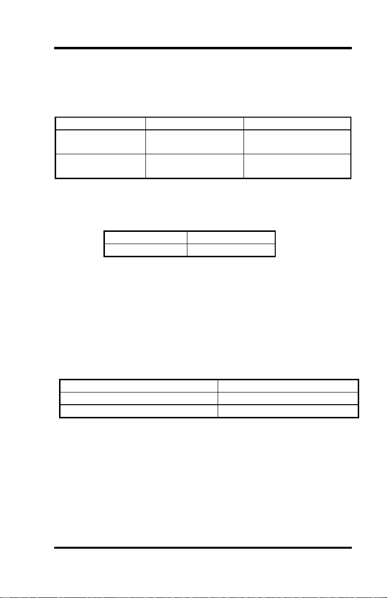
Specifications
Environmental Specifications
Specification Operating Storage
Temperature
Range
Humidity Range
Power Consumption
0º to 50º C
(32º to 122º F)
10 to 90% R.H.
Non-Condensing
(-4º to 158º F)
10 to 90% R.H.
Non-Condensing
Specifications
-20º to 70º C
Supply line
Rating
+5 VDC
195 mA
Mean Time Between Failures (MTBF)
Greater than 150,000 hours. (Calculated)
Physical Dimensions
Board length 6.2 inches (15.75 cm)
Board Height including Goldfingers 4.2 inches (10.66 cm)
Board Height excluding Goldfingers 3.9 inches (9.91 cm)
Please see Appendix G for board layout and dimensions.
Omega Engineering OMG-ACB-IV Page 13
Page 16

Appendix A - Troubleshooting
Appendix A - Troubleshooting
An ACB Developers Toolkit Diskette is supplied with the Omega
Engineering adapter and will be used in the troubleshooting procedures.
By using this diskette and following these simple steps, most common
problems can be eliminated without the need to call Technical Support.
1. Identify all I/O adapters currently installed in your system. This
includes your on-board serial ports, controller cards, sound cards etc.
The I/O addresses used by these adapters, as well as the IRQ (if any)
should be identified.
2. Configure your Omega Engineering adapter so that there is no
conflict with currently installed adapters. No two adapters can occupy
the same I/O address.
3. Make sure the Omega Engineering adapter is using a unique IRQ.
While the Omega Engineering adapter does allow the sharing of
IRQ’s, many other adapters (i.e. SCSI adapters & on-board serial
ports) do not. The IRQ is typically selected via an on-board header
block. Refer to the section on Card Setup for help in choosing an I/O
address and IRQ.
4. Make sure the Omega Engineering adapter is securely installed in a
motherboard slot.
5. Use the supplied diskette and User Manual to verify that the Omega
Engineering adapter is configured correctly. The supplied diskette
contains a diagnostic program ‘SSDACB’ that will verify if an
adapter is configured properly. Refer to the ‘UTIL.txt’ file found in
the \UTIL sub-directory on the supplied diskette for detailed
instructions on using ‘SSDACB’.
6. The following are known I/O conflicts:
• 3F8-3FF is typically reserved for COM1:
• 2F8-2FF is typically reserved for COM2:
• 3E8-3EF is typically reserved for COM3:
• 2E8-2EF is typically reserved for COM4:. This is a valid
setup option for the OMG-ACB-IV. However, since only 10
address lines are actually decoded, a possible conflict with an
advanced video card emulating the IBM XGA adapter (8514
register set) may occur.
Omega Engineering OMG-ACB-IV Page 14
Page 17

Appendix B - How To Get Assistance
Appendix B - How To Get Assistance
Please refer to Appendix A - Troubleshooting prior to calling Technical
Support.
1. Read this manual thoroughly before attempting to install the
adapter in your system.
2. When calling for technical assistance, please have your user
manual and current adapter settings. If possible, please have
the adapter installed in a computer ready to run diagnostics.
3. Omega Engineering maintains a web page on the World
Wide Web, www.omega.com, providing utilities and new
product information. This forum is accessed via the Internet.
4. Technical support is available Monday to Friday from 8:30
a.m. to 6:00 p.m. Eastern time. Technical support can be
reached at (800)826-6342 x2295.
RETURN AUTHORIZATION MUST BE OBTAINED FROM
OMEGA ENGINEERING BEFORE RETURNED MERCHANDISE
WILL BE ACCEPTED. AUTHORIZATION CAN BE OBTAINED
BY CALLING OMEGA ENGINEERING AND REQUESTING A
RETURN MERCHANDISE AUTHORIZATION (RMA) NUMBER.
Omega Engineering OMG-ACB-IV Page 15
Page 18

Appendix C - Electrical Interface
Appendix C - Electrical Interface
RS-422
The RS-422 specification defines the electrical characteristics of balanced
voltage digital interface circuits. RS-422 is a differential interface that
defines voltage levels and driver/receiver electrical specifications. On a
differential interface, logic levels are defined by the difference in voltage
between a pair of outputs or inputs. In contrast, a single ended interface,
for example RS-232, defines the logic levels as the difference in voltage
between a single signal and a common ground connection. Differential
interfaces are typically more immune to noise or voltage spikes that may
occur on the communication lines. Differential interfaces also have
greater drive capabilities that allow for longer cable lengths. RS-422 is
rated up to 10 Megabits per second and can have cabling 4000 feet long.
RS-422 also defines driver and receiver electrical characteristics that will
allow 1 driver and up to 32 receivers on the line at once. RS-422 signal
levels range from 0 to +5 volts. RS-422 does not define a physical
connector.
RS-530
RS-530 (a.k.a. EIA-530) compatibility means that RS-422 signal levels
are met, and the pin-out for the DB-25 connector is specified. The
Electronic Industry Association (EIA) created the RS-530 specification to
detail the pin-out, and define a full set of modem control signals that can
be used for regulating flow control and line status. The RS-530
specification defines two types of interface circuits, Data Terminal
Equipment (DTE) and Data Circuit-Terminating Equipment (DCE). The
Omega Engineering adapter is a DTE interface.
RS-449
RS-449 (a.k.a. EIA-449) compatibility means that RS-422 signal levels
are met, and the pin-out for the DB-25 connector is specified. The EIA
created the RS-449 specification to detail the pin-out, and define a full set
of modem control signals that can be used for regulating flow control and
line status.
Omega Engineering OMG-ACB-IV Page 16
Page 19

Appendix C - Electrical Interface
RS-485
RS-485 is backwardly compatible with RS-422; however, it is optimized
for partyline or multi-drop applications. The output of the RS-422/485
driver is capable of being Active (enabled) or Tri-State (disabled). This
capability allows multiple ports to be connected in a multi-drop bus and
selectively polled. RS-485 allows cable lengths up to 4000 feet and data
rates up to 10 Megabits per second. The signal levels for RS-485 are the
same as those defined by RS-422. RS-485 has electrical characteristics
that allow for 32 drivers and 32 receivers to be connected to one line. This
interface is ideal for multi-drop or network environments. RS-485 tri-state
driver (not dual-state) will allow the electrical presence of the driver to be
removed from the line. The driver is in a tri-state or high impedance
condition when this occurs. Only one driver may be active at a time and
the other driver(s) must be tri-stated. The output modem control signal
Request to Send (RTS) controls the state of the driver. Some
communication software packages refer to RS-485 as RTS enable or RTS
block mode transfer. RS-485 can be cabled in two ways, two wire and four
wire mode. Two wire mode does not allow for full duplex communication,
and requires that data be transferred in only one direction at a time. For
half-duplex operation, the two transmit pins should be connected to the
two receive pins (Tx+ to Rx+ and Tx- to Rx-). Four wire mode allows full
duplex data transfers. RS-485 does not define a connector pin-out or a set
of modem control signals. RS-485 does not define a physical connector.
Omega Engineering OMG-ACB-IV Page 17
Page 20

Appendix D - Direct Memory Access
Appendix D - Direct Memory Access
In many instances it is necessary to transmit and receive data at greater
rates than would be possible with simple port I/O. In order to provide a
means for higher rate data transfers, a special function called Direct
Memory Access (DMA) was built into the original IBM PC. The DMA
function allows the OMG-ACB-IV (or any other DMA compatible
interface) to read or write data to or from memory without using the
Microprocessor. This function was originally controlled by the Intel 8237
DMA controller chip, but may now be a combined function of the
peripheral support chip sets (i.e. Chips & Technology or Symphony chip
sets).
During a DMA cycle, the DMA controller chip is driving the system bus
in place of the Microprocessor providing address and control information.
When an interface needs to use DMA, it activates a DMA request signal
(DRQ) to the DMA controller, which in turn sends a DMA hold request to
the Microprocessor. When the Microprocessor receives the hold request it
will respond with an acknowledge to the DMA controller chip. The DMA
controller chip then becomes the owner of the system bus providing the
necessary control signals to complete a Memory to I/O or I/O to Memory
transfer. When the data transfer is started, an acknowledge signal
(DACK) is sent by the DMA controller chip to the OMG-ACB-IV. Once
the data has been transferred to or from the OMG-ACB-IV, the DMA
controller returns control to the Microprocessor.
To use DMA with the OMG-ACB-IV requires a thorough understanding
of the PC DMA functions. The ACB Developers Toolkit demonstrates the
setup and use of DMA with several source code and high level language
demo programs. Please refer to the SCC User’s Manual for more
information.
Omega Engineering OMG-ACB-IV Page 18
Page 21

Appendix E - Asynchronous and Synchronous Communications
Appendix E - Asynchronous and Synchronous
Communications
Serial data communications implies that individual bits of a character are
transmitted consecutively to a receiver that assembles the bits back into a
character. Data rate, error checking, handshaking, and character framing
(start/stop bits or sync characters) are pre-defined and must correspond at
both the transmitting and receiving ends. The techniques used for serial
communications can be divided two groups, asynchronous and
synchronous.
When contrasting asynchronous and synchronous serial communications,
the fundamental differences deal with how each method defines the
beginning and end of a character or group of characters. The method of
determining the duration of each bit in the data stream is also an
important difference between asynchronous and synchronous
communications. The remainder of this section is devoted to detailing the
differences between character framing and bit duration implemented in
asynchronous and synchronous communications.
Asynchronous Communications
Asynchronous communications is the standard means of serial data
communication for PC compatibles and PS/2 computers. The original PC
was equipped with a communication or COM: port that was designed
around an 8250 Universal Asynchronous Receiver Transmitter (UART).
This device allows asynchronous serial data to be transferred through a
simple and straightforward programming interface. Character boundaries
for asynchronous communications are defined by a starting bit followed by
a pre-defined number of data bits (5, 6, 7, or 8). The end of the character
is defined by the transmission of a pre-defined number of stop bits (usual
1, 1.5 or 2). An extra bit used for error detection is often appended before
the stop bits.
Omega Engineering OMG-ACB-IV Page 19
Page 22
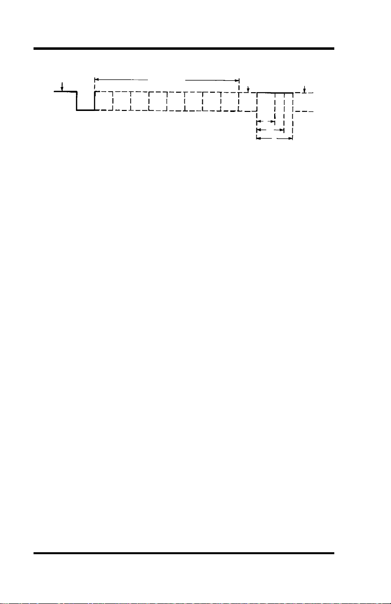
Appendix E - Asynchronous and Synchronous Communications
Remain Idle or
Idle state of
line
1
0
5 to 8 Data Bits
Odd, Even
or
Unused
P BIT
next start bit
STOP
1
1.5
2
Figure 10 - Asynchronous Communications Bit Diagram
This special bit is called the parity bit. Parity is a simple method of
determining if a data bit has been lost or corrupted during transmission.
There are several methods for implementing a parity check to guard
against data corruption. Common methods are called (E)ven Parity or
(O)dd Parity. Sometimes parity is not used to detect errors on the data
stream. This is referred to as (N)o parity. Because each bit in
asynchronous communications is sent consecutively, it is easy to
generalize asynchronous communications by stating that each character is
wrapped (framed) by pre-defined bits to mark the beginning and end of
the serial transmission of the character. The data rate and communication
parameters for asynchronous communications have to be the same at both
the transmitting and receiving ends. The communication parameters are
baud rate, parity, number of data bits per character, and stop bits (i.e.
9600,N,8,1).
Omega Engineering OMG-ACB-IV Page 20
Page 23
Appendix E - Asynchronous and Synchronous Communications
Synchronous Communications
Synchronous Communications is used for applications that require higher
data rates and greater error checking procedures. Character
synchronization and bit duration are handled differently than
asynchronous communications. Bit duration in synchronous
communications is not necessarily pre-defined at both the transmitting
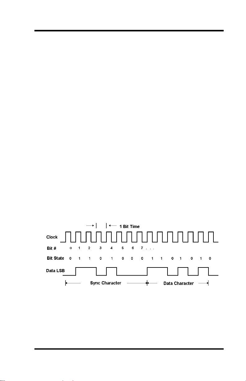
and receiving ends. Typically, in addition to the data signal, a clock signal
is provided. This clock signal will mark the beginning of a bit cell on a
pre-defined transmission. The source of the clock is predetermined and
sometimes multiple clock signals are available. For example, if two nodes
want to establish synchronous communications, point A could supply a
clock to point B that would define all bit boundaries that A transmitted to
B. Point B could also supply a clock to point A that would correspond to
the data that A received from B. This example demonstrates how
communications could take place between two nodes at completely
different data rates. Character synchronization with synchronous
communications is also very different than the asynchronous method of
using start and stop bits to define the beginning and end of a character.
When using synchronous communications a pre-defined character or
sequence of characters is used to let the receiving end know when to start
character assembly.
Figure 11 - Synchronous Communications Bit Diagram
Omega Engineering OMG-ACB-IV Page 21
Page 24

Appendix E - Asynchronous and Synchronous Communications
This pre-defined character is called a sync character or sync flag. Once
the sync flag is received, the communications device will start character
assembly. Sync characters are typically transmitted while the
communications line is idle or immediately before a block of information
is transmitted. To illustrate with an example, let's assume that we are
communicating using eight bits per character. Point A is receiving a clock
from point B and sampling the receive data pin on every upward clock
transition. Once point A receives the pre-defined bit pattern (sync flag),
the next eight bits are assembled into a valid character. The following
eight bits are also assembled into a character. This will repeat until
another pre-defined sequence of bits is received (either another sync flag
or a bit combination that signals the end of the text, e.g., EOT). The
actual sync flag and protocol varies depending on the sync format (SDLC,
BISYNC, etc.).
For a detailed explanation of serial communications, please refer to the
book Technical Aspects of Data Communications by John E. McNamara,
published by Digital Press (DEC) 1982.
Omega Engineering OMG-ACB-IV Page 22
Page 25

Appendix F - ACB Developer Toolkit Diskette and ACB Resource Kit
Appendix F - ACB Developer Toolkit Diskette and
ACB Resource Kit
The ACB Developer Toolkit diskette provides sample software, DOS and
Windows Drivers, and technical insight to aid in the development of
reliable applications for the ACB family of communication cards. The
goal in publishing this collection of source code and technical information
is two fold. First, to provide the developer with ample information to
develop ACB based applications. Second, to provide a channel for
suggestions into the technical support efforts. The ACB Resource Kit
provides a brief overview of the ACB product line and is available at your
request. Topics concerning applications and integration are covered to
provide a complete overview of the versatile ACB family. During ACB
development, if any questions, comments, or suggestions arise, please
contact Technical Support at the numbers listed at the end of this manual.
Free Updates to the ACB Developer Toolkit diskette are available at both
our CompuServe Forum (Go Sealevel) and via the Sealevel WWW Site
(www.omega.com).
Omega Engineering OMG-ACB-IV Page 23
Page 26
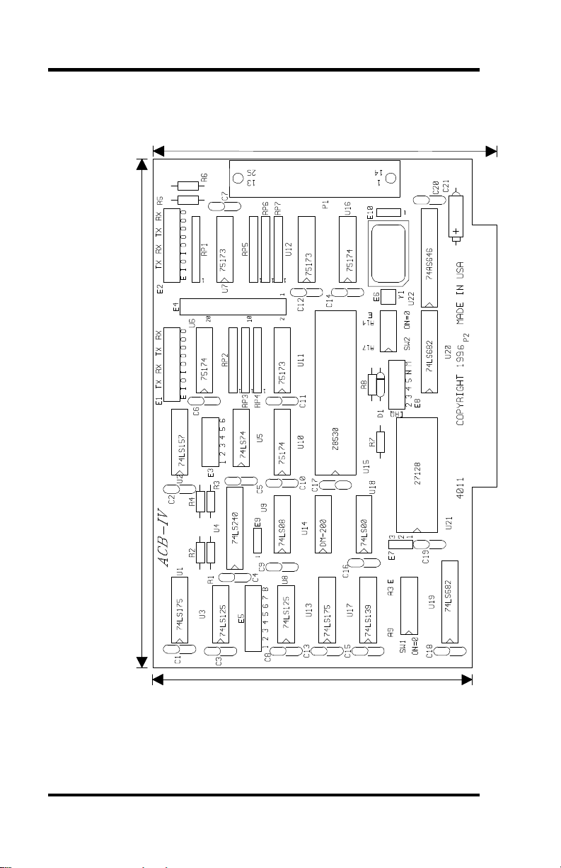
6.2"
Appendix G - Silk-Screen
Appendix G - Silk-Screen
4.2"
3.9"
Omega Engineering OMG-ACB-IV Page 24
Page 27
Appendix H - Compliance Notices
Appendix H - Compliance Notices
Federal Communications Commission Statement
FCC - This equipment has been tested and found to comply with the limits
for Class A digital device, pursuant to Part 15 of the FCC Rules. These
limits are designed to provide reasonable protection against harmful
interference when the equipment is operated in a commercial
environment. This equipment generates, uses, and can radiate radio
frequency energy and, if not installed and used in accordance with the
instruction manual, may cause harmful interference to radio
communications. Operation of this equipment in a residential area is
likely to cause harmful interference in such case the user will be required
to correct the interference at his own expense.
EMC Directive Statement
Products bearing the CE Label fulfill the requirements of
the EMC directive (89/336/EWG) and of the low-voltage
directive (73/23/EWG) issued by the European
Commission.
To obey these directives, the following European standards must be met:
• EN55022 Class A - “Limits and methods of measurement of
radio interference characteristics of information technology
equipment”
• EN50082-1 - “Electromagnetic compatibility - Generic immunity
standard”
• Part 1 : Residential, commercial and light industry
• EN60950 (IEC950) - “Safety of information technology
equipment, including electrical business equipment”
Warning
This is a Class A Product. In a domestic environment this product
may cause radio interference in which case the user may be required
to take adequate measures.
Always use cabling provided with this product if possible. If no cable is
provided or if an alternate cable is required, use high quality shielded
cabling to maintain compliance with FCC/EMC directives.
Omega Engineering OMG-ACB-IV Page 25
Page 28

Warranty
Warranty
Omega Engineering, Inc. warrants this product to be in good working
order for a period of one year from the date of purchase. Should this
product fail to be in good working order at any time during this period,
Omega Engineering will, at it's option, replace or repair it at no additional
charge except as set forth in the following terms. This warranty does not
apply to products damaged by misuse, modifications, accident or disaster.
Omega Engineering assumes no liability for any damages, lost profits, lost
savings or any other incidental or consequential damage resulting from
the use, misuse of, or inability to use this product. Omega Engineering
will not be liable for any claim made by any other related party.
RETURN AUTHORIZATION MUST BE OBTAINED FROM
OMEGA ENGINEERING BEFORE RETURNED MERCHANDISE
WILL BE ACCEPTED. AUTHORIZATION CAN BE OBTAINED
BY CALLING OMEGA ENGINEERING AND REQUESTING A
RETURN MERCHANDISE AUTHORIZATION (RMA) NUMBER.
Omega Engineering, Incorporated
PO Box 4047
One Omega Drive
Stamford, CT 06907
(800)826-6342 FAX: (203)359-7990
email: Internet: [email protected]
WWW Site: www.omega.com
Technical Support is available from 8:30 a.m. to 6 p.m. Eastern time.
Monday - Friday
Trademarks
Omega Engineering, Incorporated acknowledges that all trademarks
referenced in this manual are the service mark, trademark, or registered
trademark of the respective company.
OMG-ACB-IV is a trademark of Omega Engineering, Incorporated.
Omega Engineering OMG-ACB-IV Page 26
 Loading...