

Page 1
omega.com
e-mail: [email protected]
For latest product manuals:
omegamanual.info
Shop online at
User’s Guide
OMB-DBK Option Cards and Modules
Part 2 of 2, OMB-DBK-41 and Higher
OMB-457-0912 rev 8.1
Page 2

Servicing North America:
U.S.A.: One Omega Drive, P.O. Box 4047
ISO 9001 Certified Stamford, CT 06907-0047
TEL: (203) 359-1660 FAX: (203) 359-7700
e-mail: [email protected]
Canada: 976 Bergar
Laval (Quebec) H7L 5A1, Canada
TEL: (514) 856-6928 FAX: (514) 856-6886
e-mail: [email protected]
For immediate technical or application assistance:
U.S.A. and Canada: Sales Service: 1-800-826-6342 / 1-800-TC-OMEGA
®
Customer Service: 1-800-622-2378 / 1-800-622-BEST
®
Engineering Service: 1-800-872-9436 / 1-800-USA-WHEN
®
Mexico: En Espan˜ ol: (001) 203-359-7803 e-mail: [email protected]
FAX: (001) 203-359-7807 [email protected]
Servicing Europe:
Benelux: Postbus 8034, 1180 LA Amstelveen, The Netherlands
TEL: +31 (0)20 3472121 FAX: +31 (0)20 6434643
Toll Free in Benelux: 0800 0993344
e-mail: [email protected]
Czech Republic: Frystatska 184, 733 01 Karviná, Czech Republic
France: 11, rue Jacques Cartier, 78280 Guyancourt, France
TEL: +33 (0)1 61 37 2900 FAX: +33 (0)1 30 57 5427
Toll Free in France: 0800 466 342
e-mail: [email protected]
Germany/Austria: Daimlerstrasse 26, D-75392 Deckenpfronn, Germany
TEL: +49 (0)7056 9398-0 FAX: +49 (0)7056 9398-29
Toll Free in Germany: 0800 639 7678
e-mail: [email protected]
United Kingdom: One Omega Drive, River Bend Technology Centre
ISO 9002 Certified Northbank, Irlam, Manchester
M44 5BD United Kingdom
TEL: +44 (0)161 777 6611 FAX: +44 (0)161 777 6622
Toll Free in United Kingdom: 0800-488-488
e-mail: [email protected]
OMEGAnet®Online Service Internet e-mail
omega.com [email protected]
It is the policy of OMEGA Engineering, Inc. to comply with all worldwide safety and EMC/EMI
regulations that apply. OMEGA is constantly pursuing certification of its products to the European New
Approach Directives. OMEGA will add the CE mark to every appropriate device upon certification.
The information contained in this document is believed to be correct, but OMEGA accepts no liability for any
errors it contains, and reserves the right to alter specifications without notice.
WARNING: These products are not designed for use in, and should not be used for, human applications.
Page 3
Warnings, Cautions, Notes, and Tips
Refer all service to qualified personnel. This symbol warns of possible personal injury or equipment damage under
noted conditions. Follow all safety standards of professional practice and the recommendations in this manual. Using
this equipment in ways other than described in this manual can present serious safety hazards or cause equipment
damage.
This warning symbol is used in this manual or on the equipment to warn of possible injury or death from electrical
shock under noted conditions.
This ESD caution symbol urges proper handling of equipment or components sensitive to damage from electrostatic
discharge. Proper handling guidelines include the use of grounded anti-static mats and wrist straps, ESD-protective
bags and cartons, and related procedures.
This symbol indicates the message is important, but is not of a Warning or Caution category. These notes can be of
great benefit to the user, and should be read.
In this manual, the book symbol always precedes the words “Reference Note.” This type of note identifies the location
of additional information that may prove helpful. References may be made to other chapters or other documentation.
Tips provide advice that may save time during a procedure, or help to clarify an issue. Tips may include additional
reference.
Specifications and Calibration
Specifications are subject to change without notice. Significant changes will be addressed in an addendum or revision to
the manual. As applicable, we calibrate our hardware to published specifications. Periodic hardware calibration is not
covered under the warranty and must be performed by qualified personnel as specified in this manual. Improper
calibration procedures may void the warranty.
iii
Page 4
Your order was carefully inspected prior to shipment. When you receive your order, carefully
unpack all items from the shipping carton and check for physical signs of damage that may have
occurred during shipment. Promptly report any damage to the shipping agent and your sales
representative. Retain all shipping materials in case the unit needs returned to th e factory.
CAUTION
Using this equipment in ways other than described in this manual can cause
personal injury or equipment damage. Before setting up and using your
equipment, you should read all documentation that covers your system.
Pay special attention to Warnings and Cautions.
Note:
During software installation, Adobe
®
PDF versions of user manuals will automatically
install onto your hard drive as a part of product support. The default location is in the
Programs group, which can be accessed from the Windows Desktop. Initial
navigation is as follows:
Start [Desktop “Start” pull-down menu]
⇒ Programs
⇒ Omega DaqX Software
You can also access the PDF documents directly from the data acquisition CD by using
the <View PDFs> button located on the opening screen.
Refer to the PDF documentation for details regarding both hardware and software.
®
A copy of the Adobe Acrobat Reader
is included on your CD. The Reader provides
a means of reading and printing the PDF documents. Note that hardcopy versions of
the manuals can be ordered from the factory.
iv
Page 5

DBKs Covered in Part 2 of 2 (with exception of DBK70)
DBK41, 10-Slot Expansion Module
DBK42, 16-Slot 5B Signal Conditioning Module
DBK43A, 8-Channel Strain-Gage Module
DBK44, 2-Ch. 5B Signal-Conditioning Card
DBK45, 4-Ch. SSH and Low-Pass Filter Card
DBK46, 4-Channel Analog Output Card
DBK48, Multipurpose Isolated Signal-Conditioning Module (supports up to 16 8B Modules)
DBK50 and DBK51, Voltage Input Modules
DBK55, 8-Channel Frequency-to-Voltage Input Module
DBK60, 3-Slot Expansion Chassis
DBK65, 8-Channel Transducer Interface Module
DBK80, 16-Ch. Differential Voltage Input Card with Excitation Output
DBK81, 7-Ch. T/C Card
DBK82, 14-Ch. T/C Card
DBK83, 14-Ch. T/C Card, uses external connection pod
DBK84, 14-Ch. T/C Module
DBK85, 16-Ch. Differential Voltage Module
DBK90, 56-Ch. T/C Module
DBK100 Series, (DBK100/D, 100/T,101)
In-Vehicle Thermocouple Measurement System
DBK200 Series Matrix
DBK200, P4-to-P1 Adapter Board
DBK202, DBK203, DBK204 Series
P4-to-P1/P2/P3 Adapters
DBK206, P4-to-P1/P2/P3 Adapter Board with Screw Terminals
DBK207 and DBK207/CJC, 16-Channel,
5B Carrier Boards
DBK208, Relay Carrier Board,
Opto-22 Compatible
DBK209, P4 to P1/P2/P3 Mini-Adapter Board
DBK210, 32-Ch. Digital I/O Carrier Board
DBK213, Screw-Terminal & Expansion Module
3-Card Slot, P1/P2/P3/P4 Compatibility
DBK214, 16-Connector BNC Interface Module
P1/P2/P3/P4 Compatibility
DBK215, 16-Connector BNC Connection Module
with 68-Pin SCSI Adaptability
DBK601 thru DBK609, Termination Panels
967194 DBK Cards & Modules
Page 6

Discontinued DBKs
The following DBKs have been discontinued. However, documentation
for them may be obtained from the factory.
DBK12 and DBK13, A/I Multiplexer Cards
DBK19, 14-Channel Thermocouple Card
DBK33, Triple-Output Power Supply Card
DBK34, Vehicle UPS Module
DBK40, 18-Connector BNC Analog Interface
DBK52, 14-Ch. Thermocouple Input Module
DBK53 and DBK54, Analog Multiplexing Modules
DBK201, P4-to-P1/P2/P3 Adapter Board
DBK603, Termination Panel, Safety Jacks, SE
DBK605-B, Termination Panel, T/C, B Type, DE
DBK605-R, Termination Panel, T/C, R Type, DE
DBK605-S, Termination Panel, T/C, S Type, DE
DBK605-U, Termination Panel, T/C, U Type, DE
DBK609, Termination Panel, 5-Pin DIN
iv 917594 DBK Option Cards & Modules User’s Manual
Page 7
DBK41 10-Slot Expansion Module
Overview …… 1
Hardware Setup …… 2
Card Configuration …… 2
Power Configuration …… 2
Card Insertion …… 3
EMI Shield Plates for CE Compliance …… 4
System Connection …… 5
DBK41 – Specifications …… 5
Overview
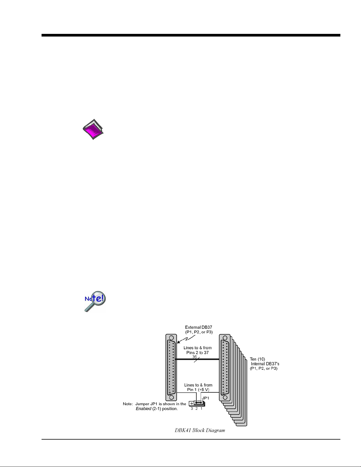
The DBK41 is a metal enclosure that holds up to 10 DBK cards. The exterior front panel has a male DB37
connector that leads to the LogBook or Daq device or further expansion via a CA-37-x cable. On the
inside of the front panel, a backplane printed circuit board (PCB) uses 10 female DB37s with their pins
connected in parallel to distribute the P1 interface (can also be used with P2 or P3). From the rear panel,
the DBKs’ signal input lines exit to their respective transducers.
Reference Notes:
o Chapter 2 includes pinouts for P1, P2, P3, and P4. Refer to pinouts applicable to your
system, as needed.
o In regard to calculating system power requirements, refer to DBK Basics located near
the front of this manual.
An optional EMI kit provides shield plates for the rear panel to make the DBK41 CE-compliant and
prevent EMI from DBKs entering the test environment (or vice-versa). The EMI kit also functions as an
electrical safety barrier.
Some DBK cards require a lot of power, in relation to other cards, and the use of power is an important
concern. DBK cards can obtain power externally from a LogBook, DaqBook, DaqBoard; or internally
from a DBK32A or DBK33 card. Refer to Power Requirements in the DBK Basics section, as well as the
sections for the DBK32A and/or DBK33, as applicable.
A power card in any slot (other than the slot leftmost from rear view) will power the
other cards via the backplane. A front panel LED will light whenever power from any
source is on the backplane. DBK41’s JP1 jumper can be positioned to disable the +5 V
power line from the external DB37. This prevents a DBK33 power supply from
interfering with other devices.
DBK Option Cards and Modules 877095 DBK41, pg. 1
Page 8
Hardware Setup
Setup concerns include card and power configuration, proper card insertion, the use of EMI shields for CE
compliance, and mounting [or stacking] of hardware components.
In regard to mounting: metal splice plates can be used to rigidly mount a LogBook or DaqBook on top of a
DBK41 or other device that shares the same footprint. For applications in which temporary mounting is
convenient: a LogBook, DaqBook or notebook PC can be temporarily mounted to a DBK41 with the use
of industrial-strength dual-lock pads or strips.
Card Configuration
Each DBK card should be checked for proper configuration, and re-configured if needed, before being
inserted into the DBK41. Refer to the individual DBK Document Modules that are applicable to your
system.
Power Configuration
Power must be configured to prevent multiple power supplies from interfering with each other via the P1
interface. DBK41, LogBook/360, DaqBook/100 Series & /200 Series, and ISA-type DaqBoard each have
JP1 jumpers that must be properly configured in regard to power. Details for each follow.
JP1 in the DBK41
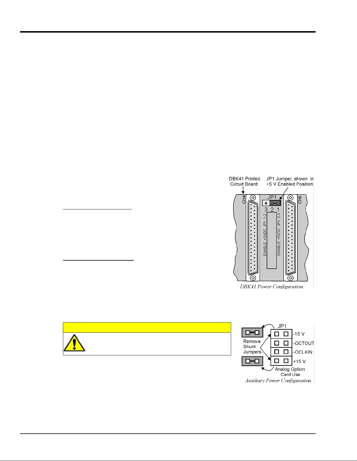
On the DBK41 backplane, JP1 is a 3-pin jumper positioned between
DB37 connectors for card number 4 (CN4) and card number 5
(CN5). Two settings are possible, as follows:
ENABLE +5 VDC JP1 1-2
When JP1 pins 1 and 2 are jumpered, the +5 VDC line to the
external P1 connector is enabled. The 5 V (VCC) is externally
supplied to pin 1 for cards 1 through 10 (CN1 through CN10). The
+5 VDC power can come from a LogBook, DaqBook, or DaqBoard
through a CA-37-x cable on pin 1 of P1. If not using a DBK33, JP1
should be enabled.
DISABLE +5 VDC JP1 2-3
When JP1 pins 2 and 3 are jumpered, the +5 VDC line to the
external P1 connector is disabled. When using a DBK33 power
card in the DBK41, the JP1 jumper must be set on pin 2 and 3. The
JP1 2-3 setting prevents the DBK33’s +5 V from interfering with
external devices via the P1 interface.
JP1 in the DaqBook/100 Series & /200 Series and DaqBoard [ISA type]
CAUTION
DBK power cards must not be connected until JP1
jumpers have been removed. Otherwise, equipment
damage could result.
If a DBK32A or DBK33 is used, you must remove the shunt jumpers
from the JP1 header located inside the DaqBook/100 Series & /200 Series
device or DaqBoard [ISA type]. DaqBook/100 Series & /200 Series
devices and DaqBoards [ISA type] are shipped with these shunts
positioned to deliver ±15 V analog power to P1.
Note: The jumpers can be placed on the -OCTOUT and -OCLKIN pins but should be removed if there is
interference with card operation (counter-timer).
DBK41, pg. 2 877095 DBK Option Cards and Modules
Page 9
JP1 and JP2 in LogBook/360
Proper jumper configuration limits LogBook/360’s P1 bus to one power source. There should never be
more than one power source. The jumpers are located inside the chassis, on the unit’s P1 Interconnect
Board.
JP1. Only remove LogBook/360’s JP1 jumper if a DBK33 is used with the system.
JP2. Only remove the LogBook/360’s JP2 jumper if DBK cards are to be powered from LogBook/360’s
DaqBook/2000 Series & DaqBoard/2000 Series Configuration
No jumper configurations are required for these /2000 series devices.
Card Insertion
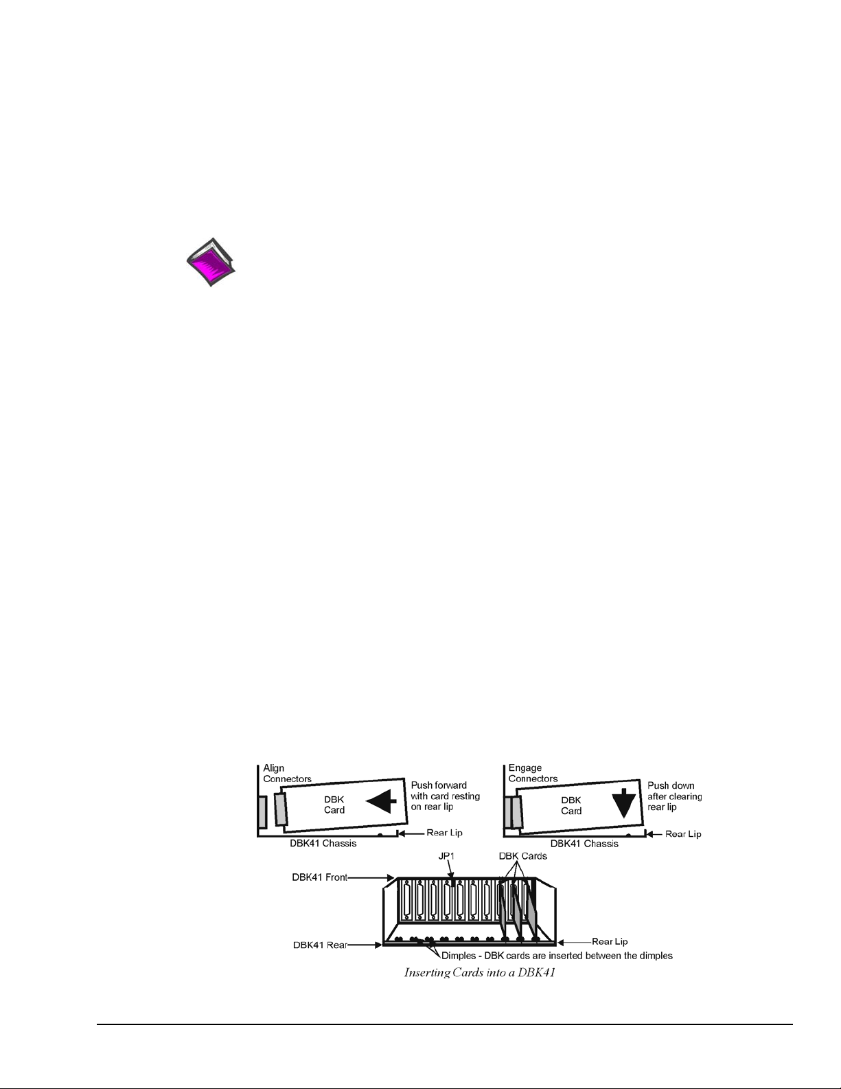
Each DBK card has a DB37 male connector which mates with the DB37 female connectors inside the
DBK41 chassis. To insert DBK cards into the DBK41 chassis, refer to the figure and perform the
following steps.
Note: Cards using screw-connectors for signal input lines must be wired before insertion.
1. Disconnect power from all units to be connected.
internal PCB.
Reference Note:
Refer to the LogBook User’s Manual, 461-0901 for information regarding LogBook systems.
2. Place the DBK41 on a flat surface; loosen the two thumbscrews on rear of the case; and remove the
top cover by sliding it off.
3. Align the DBK card with the DBK41 connector to be used (CN1 to CN10). The first slot must always
be occupied; however, a DBK32A or DBK33 power card may not occupy the first slot. Any of the
remaining 9 slots can be used or unused.
4. To clear the lip on the rear panel, tilt the rear of the card upward. Engage the P1 connectors of the
card and chassis, and press together gently to avoid damage to the pins.
5. Press down the rear of the card, aligning it within the metal dimples at the rear of the DBK41.
6. After cards are in place, reassemble the DBK41’s top cover and attach optional shield plates
(described next); then re-connect and power up the system.
DBK Option Cards and Modules 877095 DBK41, pg. 3
Page 10
EMI Shield Plates for CE Compliance
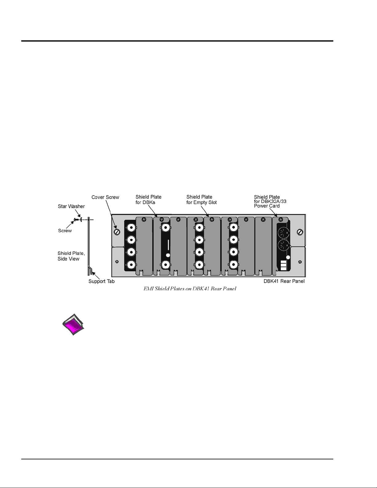
To reduce electro-magnetic interference (EMI) escaping from (or entering into) the enclosure, a CE kit
provides shield plates that attach to the rear of the DBK41. The kit also functions as an electrical safety
barrier. With shield plates attached (a combination of 3 types supplied), the system meets CE standards.
The kit includes:
• Full shield plates to cover empty (unused) slots
• Partial shield plates to surround DBKs in a slot (except a power card)
• Partial shield plates to surround a DBK32A or DBK33 power card
• Screws and star washers to secure the shields to the chassis
Note: The CE kit is included with the DBK41/CE and an optional accessory for a DBK41.
The shields have a support tab that slides over the edge of the bottom plate and a screw hole for
attachment to the top plate. When tightened, the screws cause the washers to pierce the surface
coating into the metal to make a good contact with chassis ground.
Reference Note:
The Signal Management chapter contains additional information pertaining to CE Compliance.
DBK41, pg. 4 877095 DBK Option Cards and Modules
Page 11
System Connection
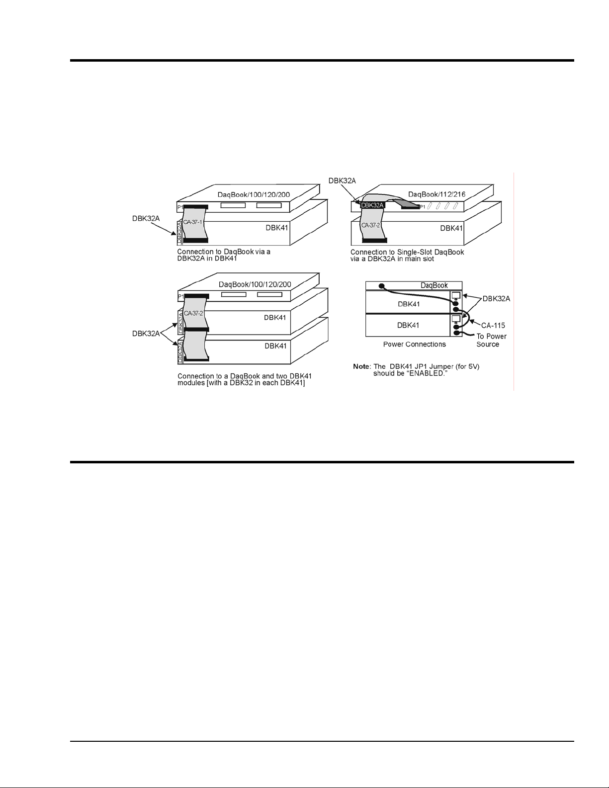
A short ribbon cable (CA-37-x) attaches the DBK41 to the main unit. Connecting the DBK41 to any port
other than P1 may damage devices in the system. Likewise, only analog expansion cards may be installed
in the DBK41.
Note: For CE compliance, the CA-37-x cable must be replaced with a CA-143-7 or
CA-143-18. Multiple chassis require a “T” connector (part # CN-143) for branching.
Examples of DBK41 Connections [with DBK32A] and Cascading Power
DBK41 - Specifications
Name/Function: 10-Slot Analog Expansion Module
Card Capacity: 10 slots to hold standard DBK option cards
Weight: 4 lb (with no cards installed)
Cable (optional): 8" ribbon with DB37 female to DB37 female (CA-37-x)
Power Indicator: LED powered by external device’s 5 VDC
Connection: Male DB37, mates via CA-37-x cable with P1
DBK Option Cards and Modules 877095 DBK41, pg. 5
Page 12

DBK41, pg. 6 877095 DBK Option Cards and Modules
Page 13
DBK42 16-Slot 5B Signal Conditioning Module
Overview …… 1
Hardware Setup …… 2
DBK42 Connection …… 2
DBK42 Configuration …… 2
5B Module Connection …… 2
Power Considerations …… 2
Terminal Block Connections …… 3
DaqBoard/2000 Series and cPCI DaqBoard/2000c Series Connections …… 5
DaqBook/100 Series & /200 Series and ISA-Type DaqBoard Configuration …… 5
DaqBook/2000 Series and DaqBoard/2000 Series Configuration …… 5
Software Setup …… 6
DBK42 – Specifications …… 8
Reference Notes:
o Chapter 2 includes pinouts for P1, P2, P3, and P4. Refer to pinouts applicable to your
Overview
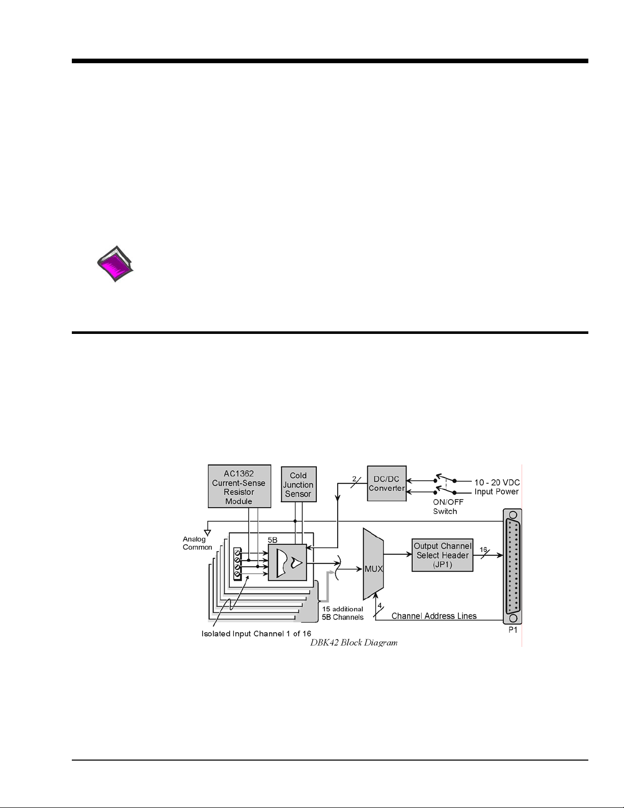
The DBK42 allows LogBook or Daq device systems to work with up to 16 5B signal conditioning
modules. Modules are available for various signal types (e.g., low-level thermocouple signals, strain-gage
signals, etc). The DBK42 offers 500 V isolation from the system and between channels. The DBK42 is
compatible with all 5B output modules, and the configuration is very flexible. You can select the type of
signal attached to each channel.
system, as needed.
o In regard to calculating system power requirements, refer to DBK Basics located near
the front of this manual.
An accessory cable connects the DBK42’s output to the P1 analog input connector. One LogBook or Daq
device can support up to 16 DBK42 units with a maximum of 256 isolated analog input channels. The
LogBook or Daq device scans the DBK42 channels at the same 10 µs/channel rate as other DBKs (256
scans in 2.56 ms in a full system).
The DBK42 can obtain power from an included AC adapter, an optional DBK30A rechargeable battery
module, or directly from a 12 VDC source (such as a car battery). The built-in power supply can serve a
fully-configured system using bridge excitation.
For DaqBoard/2000 Series applications, DBK42 is typically powered from an included AC adapter. The
unit’s built in power supply can serve a fully-configured system using bridge excitation.
DBK Option Cards and Module 967694 DBK42, pg. 1
Page 14
Each terminal block contains 4 terminals (per channel) for access to input and excitation features of 5B
modules.
The optional CN-71 and CN-72 signal connection blocks provide a convenient way of connecting analog
signals to the DBK42.
• The CN-71 is for non-thermocouple use.
• The CN-72 (with cold junction sensors) is for thermocouple use. The CN-72 has a clear
Hardware Setup
DBK42 Connection
The DBK42 has screw-terminal connectors for easy access to the analog inputs. 2-wire and 4-wire
hookups are shown later in this section.
Note: Analog channels are isolated from each other, and no analog ground is provided.
DBK42 Configuration
Up to 16 DBK42s can connect to a LogBook or a Daq device. As a daisy-chain interface,
each module must appear unique and use a different channel.
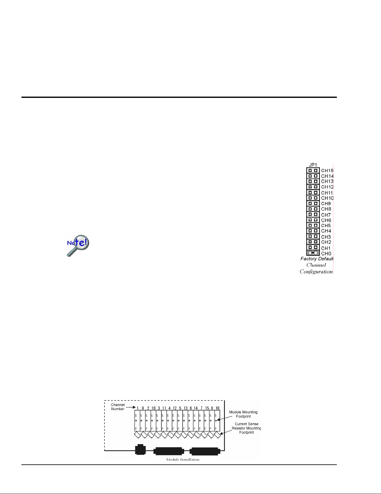
To configure the module, locate the 16×2-pin header (JP1) near the front of the DBK42
board. Note the 16 jumper locations labeled CH0 through CH15 representing the base
Analog Input Channels. Place the jumper on the channel you wish to use.
plastic shield over its screw terminals to protect you from high voltage on the input terminals.
Only one jumper is used on a single DBK42. No two cards in a system
can use the same JP1 setting.
5B Module Connection
Each input of the DBK42 is processed through a user-installed 5B signal-conditioning module. Different
5B modules are used with different transducer and signal sources. To install the modules:
1. Match the footprint of the module with the footprint on the circuit board (see figure).
2. Gently place the module into the footprint, and screw it down.
3. When installing current input modules (SC-5B32 series), install the supplied current-sense resistor
(SC-AC-1362) in the resistor footprint adjacent to the module mounting footprint.
4. Record the module’s channel number; label all units and connectors for identification.
Power Considerations
The DBK42 has an internal, isolated switching-type power supply that operates on 10-20 VDC at varying
input currents depending on the input voltage and 5B-module loading. The power drain at a given output
load is constant; input current will vary inversely with the input voltage.
DBK42, pg. 2 967694 DBK Option Cards and Modules
Page 15
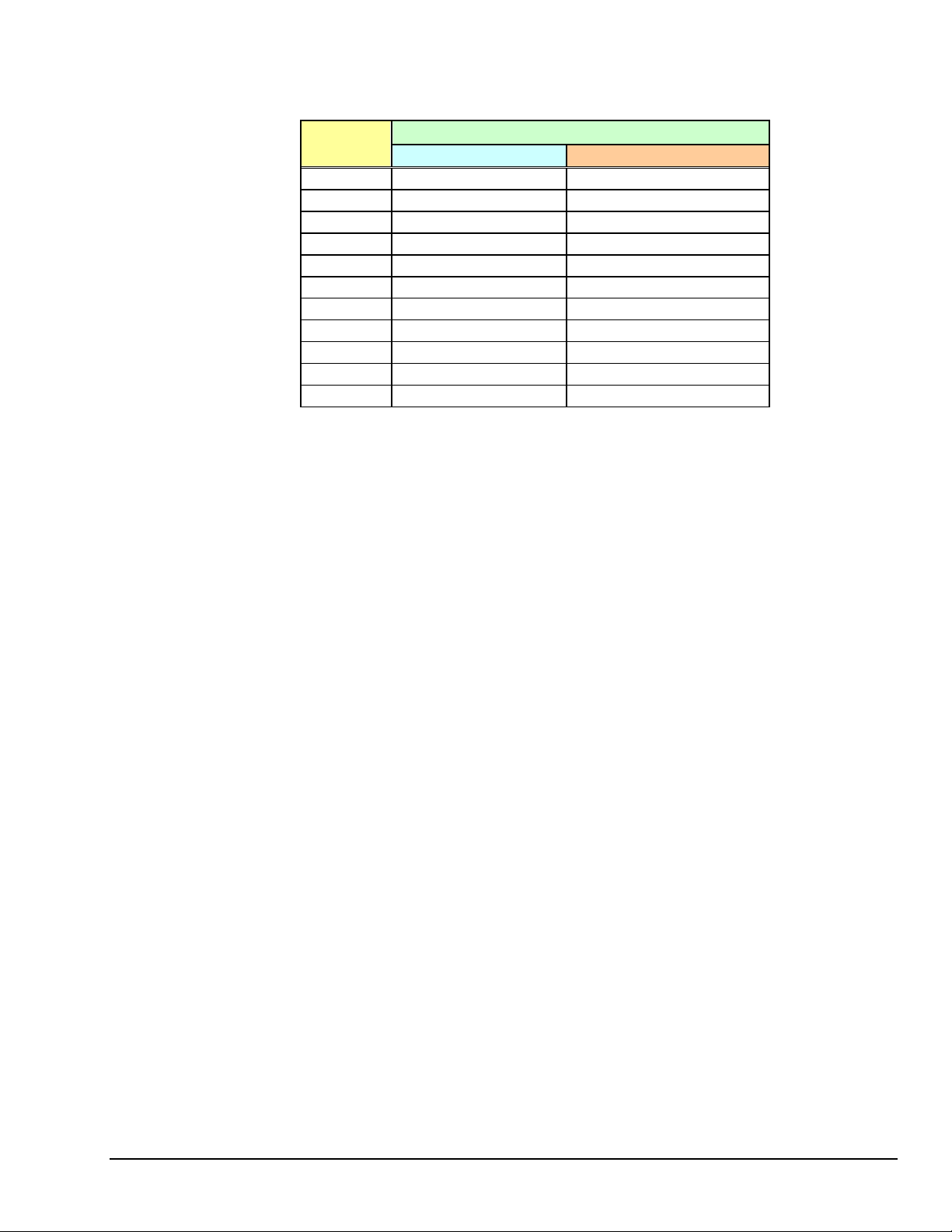
A DBK42 populated with strain-gage modules will draw more current than with other types of input
modules. The table shows the DC input requirements for the worst-case setup (with 16 strain-gage
modules or 16 thermocouple modules).
Input Volts
With Strain-Gage Modules With Thermocouple Modules
10 VDC 3.0 A 0.60 A
11 VDC 2.7 A 0.54 A
12 VDC 2.4 A 0.48 A
13 VDC 2.2 A 0.44 A
14 VDC 2.0 A 0.40 A
15 VDC 1.9 A 0.38 A
16 VDC 1.8 A 0.36 A
17 VDC 1.7 A 0.34 A
18 VDC 1.6 A 0.32 A
19 VDC 1.5 A 0.30 A
20 VDC 1.4 A 0.28 A
Input Amperes
Power sources include:
• The standard TR-25 AC plug-in power pack (provided with the DBK42) can supply 900 mA at
15 VDC. The optional TR-40U can supply 2700 mA at 15 VDC.
• The DBK30A battery pack can supply power for a typical DBK42 configuration; however, in a
fully-populated strain-gage configuration, the battery run-time will be limited to about 1½ hours.
• A 12 V lead-acid gel-cell type battery can easily power a fully-populated strain-gage
configuration. The battery drain will be about 2.4 A-hr; battery size should be considered for
systems with long run-times. (For example, a common-size 5.0 A-hr battery will operate for
about 2 hours). A typical automotive 12-V lead-acid battery (e.g., 60 A-hr) can easily power a
DBK42 for long run-times (about 24 hours).
The input fuse is a 4-A Slo-Blo 1-1/4" × 1/4" glass-type such as Littelfuse 313004 or Bussman MDL-4.
Terminal Block Connection
Input signals (and excitation leads) must be wired to the DBK42 signal termination panel. Sixteen
4-terminal blocks accept up to 16 inputs. These connectors are located on a removable PC board that plugs
into two DIN96 rectangular connectors on the rear panel.
Terminal blocks are connected internally to their corresponding signal conditioning module. The terminal
blocks accept up to 14-gage wire into quick-connect screw terminals. Terminals on each block are
numbered 1 through 4. Each type of input signal or transducer (such as a thermocouple or strain gage)
should be wired to its terminal block as shown in the figure. Wiring is shown for RTDs, thermocouples,
20 mA circuits, mV/V connections, and for full- and half-bridge strain gages.
DBK Option Cards and Module 967694 DBK42, pg. 3
Page 16
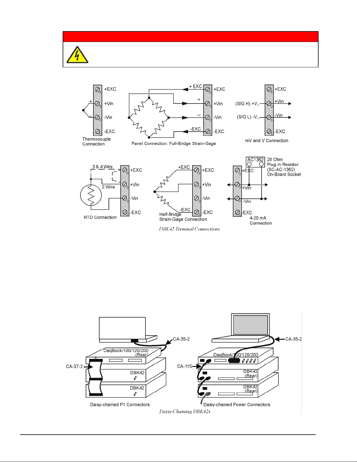
Shock Hazard! The DBK42 is designed to sense signals that may carry dangerous
voltages. De-energize circuits connected to the DBK42 before changing the wiring or
configuration.
WARNING
P1 Connection. The DBK42 attaches to the P1 analog I/O connector or to a DBK200 series P4-Adapter
P1 analog I/O connector. (Up to 16 units can be attached to one LogBook or Daq device.) Connect the
appropriate ribbon cable (with -x indicating the number of cards to be connected) from the LogBook,
Daq device, or adapter P1 port to the DB37 connector at the end of the option card.
Note: A series of interface cables are available for connecting up to sixteen DBK42s.
DBK42, pg. 4 967694 DBK Option Cards and Modules
Page 17
DaqBoard/2000 Series and cPCI DaqBoard/2000c Series Connections
DBK42 can be connected to the P1 connector of DaqBoard/2000 Series P4-adapters. Up to 16 units can be
attached to one DaqBoard/2000 Series board.
Connect the appropriate ribbon cable (with -x indicating the number of cards to be connected) from the
adapter’s P1 port to the DB37 connector at the end of the option card.
Note: A series of interface cables is available for connecting up to 16 DBK42s.
DaqBook/100 Series & /200 Series and ISA-Type DaqBoard Configuration
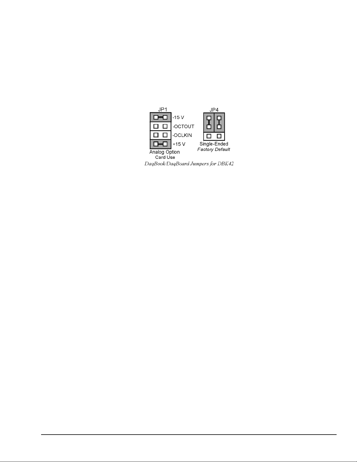
The DBK42 requires two setup steps in DaqBook/100 Series & /200 Series devices and DaqBoards
[ISA type]—jumpers JP1 and JP4.
1. If not using auxiliary power, place the JP1 jumper in the expanded analog mode.
Note: This default position is necessary to power the interface circuitry of the DBK42 via the internal
±15 VDC power supply. If using auxiliary power (DBK32A, or DBK33), you must remove
both JP1 jumpers. Refer to Power Requirements in the DBK Basics section of the manual.
Also, refer to the DBK32A and DBK33 sections as applicable.
2. For DaqBook/100, /112, and /120 only, place the JP4 jumper in the DaqBook/100 & /200
or ISA-type DaqBoard in single-ended mode. Analog expansion cards convert all input signals to
single-ended voltages referenced to analog common.
DaqBook/2000 Series and DaqBoard/2000 Series Configuration
No Jumper configurations are required for these /2000 series devices.
DBK Option Cards and Module 967694 DBK42, pg. 5
Page 18
Software Setup
You will need to set several parameters so DaqView can best meet your application requirements.
After the 5B module type is identified, DaqView figures out the m and b (of the mx+b equation) for proper
engineering units scaling. An example of the mx + b equation follows shortly.
The mx + b calculations for most 5B modules are included within LogView software.
PDF Note:
Reference Note:
o For DaqView information refer to chapter 3, DBK Setup in DaqView and to the DaqView
PDF included on your data acquisition CD.
o For LogView information refer to chapter 4, DBK Setup in LogView and to the LogView
section of the LogBook PDF included on your data acquisition CD.
o The API includes functions applicable to the DBK42. Refer to related material in the
Programmer’s Manual (p/n 1008-0901) as needed.
®
During software installation, Adobe
PDF versions of user manuals automatically install onto
your hard drive as a part of product support. The default location is in the Programs group,
which can be accessed from the Windows Desktop. Refer to the PDF documentation for
details regarding both hardware and software. Note that you can also access PDF documents
directly from the data acquisition CD via the <View PDFs> button on the CD’s opening
screen.
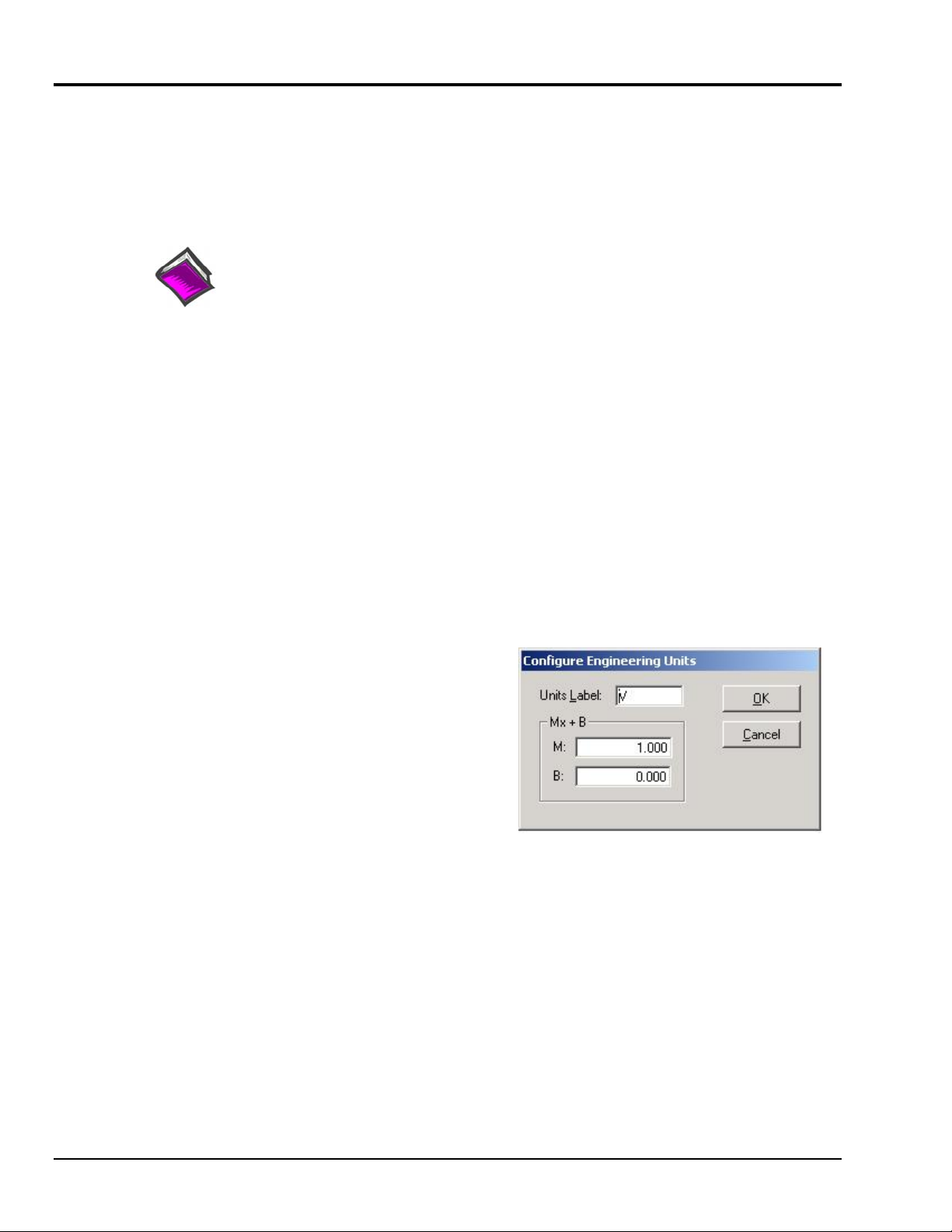
mX +b, an Example
The Customize Engineering Units dialog box can be
accessed via the DaqView Configuration main
window by activating the Units cell [for the desired
channel], then clicking to select mX+b.
From the Customize Engineering Units dialog box
(see figure at right), you can enter values for m and b
components of the equation that will be applied to
the data. There is also an entry field that allows you
to enter a label for the new units that may result from
the mX+b calculation.
An example of mX + b equation use follows.
DBK42, pg. 6 967694 DBK Option Cards and Modules
Page 19

Engineering Units Conversion Using mx + b
Most of our data acquisition products allow the user to convert a raw signal input (for example, one that is
in volts) to a value that is in engineering units (for example, pressure in psi). The products accomplish this
by allowing the user to enter scale and offset numbers for each input channel, using the software associated
with the product. Then the software uses these numbers to convert the raw signals into engineering units
using the following “mx + b” equation:
(1) Engineering Units = m(Raw Signal) + b
The user must, however, determine the proper values of scale (m) and offset (b) for the application in
question. To do the calculation, the user needs to identify two known values: (1) the raw signal values, and
(2) the engineering units that correspond to the raw signal values. After this, the scale and offset
parameters can be calculated by solving two equations for the two unknowns. This method is made clear
by the following example.
Example
An engineer has a pressure transducer that produces a voltage output of 10.5 volts when the measured
pressure is 3200 psi. The same transducer produces an output of 0.5 volt when the pressure is 0 psi.
Knowing these facts, m and b are calculated as follows.
A - Write a pair of equations, representing the two known points:
(2) 3200 = m(10.5) + b
(3) 0 = m(0.5) + b
B - Solve for m by first subtracting each element in equation (3) from equation (2):
(4) 3200 - 0 = m(10.5 – 0.5) + (b - b)
(5)
Simplifying gives you: 3200 = m(10)
(6)
This means: m = 320
C - Substitute the value for m into equation (3) to determine the value for b:
(7) 0 = 320 (0.5) + b
(8)
Therefore: b = - 160
Now it is possible to rewrite the general equation (1) using the specific values for m and b that we just
determined:
(9) Engineering Units = 320(Raw Signal) - 160
The user can then enter the values of m and b into the appr opriate location using the facilities provided by
compatible data acquisition software, for example: WaveView, DaqView, Personal DaqView, LogView, and
TempView. The software uses equation (9) to calculate signal values in engineering units from that point
on.
DBK Option Cards and Module 967694 DBK42, pg. 7
Page 20

DBK42 – Specifications
Name/Function: 16-Slot 5B Signal Conditioning Module
Module Capacity: 16 (input only) 5B modules
Size: 8.5" × 11" × 3.5" (11" × 11" × 3.5" with optional CN-71 or CN-72)
Weight: 4 lb (with no modules installed)
Cable (optional): CA-37-1
Power Requirements: 10-24 VDC @ 2.6 - 0.3 A
With 16 thermocouple-type modules:
12 VDC @ 0.50 A
15 VDC @ 0.40 A
18 VDC @ 0.35 A
With 16 strain-gage type modules:
12 VDC @ 1.9 A
15 VDC @ 1.5 A
18 VDC @ 1.3 A
DC Input Fuse: 3A
Power Indicator: LED powered by internal 5 VDC
Power Connection: DIN5 ×2 for daisy-chaining
AC Power Pack::
120 VAC to 15 VDC converter
120 VAC to 15 VDC @ 2.0 A (optional)
Input Connections: DIN96 rectangular, standard, screw terminal adapter (optional)
Connection: Male DB37 mates via CA-37-1 cable with P1
DC/DC Converter: 10-24 VDC to 5 VDC (isolated)
Isolation:
Input Power to System: 500 VDC
Signal Inputs to System: 1500 VDC
Input Channel-to-Channel: 500 VDC
DBK42, pg. 8 967694 DBK Option Cards and Modules
Page 21

DBK43A 8-Channel Strain Gage Module
Overview …… 1
Hardware Connection …… 3
Power Connection …… 3
Signal Connection …… 4
Hardware Configuration …… 4
Bridge Applications …… 5
AC Coupling and Low-Pass Filter Options …… 10
P1 Output Channel and Card Address Selection …… 11
DaqBook/100 Series & /200 Series and DaqBoard [ISA type] Configuration …… 11
DaqBook/2000 Series and DaqBoard/2000 Series Configuration …… 12
Hardware Adjustment …… 12
Trimpots …… 12
CAL/NORM Switch …… 12
Software-Controlled Setup …… 13
Selecting Channel Types in DaqView ……13
Selecting Channel Modes in LogView……14
A Typical Setup Procedure with Embedded Examples ……15
GageCal, Calibration Program for DBK16 and DBK43A in Daq Applications ……19
Calibrating DBK16 and DBK43A for LogBook Applications ……23
Overview …… 23
Calibration Methods …… 24
Procedures Common to All Calibration Steps (Required) …… 25
Nameplate Calibration and Manual Calibration …… 28
Channel Calibration Procedure …… 31
2-Point Calibration …… 34
Shunt Calibration …… 36
Creating a Units Conversion Transfer Function …… 38
Periodic Calibration Without Trimpots …… 38
DBK43A – Specifications …… 39
Note: Because of the DBK43A’s flexibility in configuration, please review the entire section before
Reference Notes:
o In regard to calculating system power requirements, refer to the section Power
Requirements in the DBK Basics section located at the beginning of the manual.
o Chapter 2, System Connections and Pinouts, includes pinouts for P1, P2, P3, and
P4. Refer to the pinouts that are applicable to your system, as needed.
attempting setup and operation.
Overview
The DBK43A will condition signals from most bridge-circuit transducers that have a signal output of less
than 50 mV. Strain gages and load cells are common types. As needed, refer to the block diagram (below)
and the board layout (later).
For half-bridge and quarter-bridge strain gages, the DBK43A can accommodate usersupplied BCRs (bridge-completion resistors) that complete the bridge circuit. The bridge
circuit must be complete for the DBK43A to operate correctly.
Each channel of the DBK43A offers a selectable 3-pole, low-pass filter with a user-set cut-off frequency.
Remote-sense terminals are provided to make 6-wire Kelvin connections. Up to 2 DBK43A modules can
be connected to each of 16 analog base channels for up to 256 input signals.
DBK Option Cards and Module 877095 DBK 43A, pg. 1
Page 22
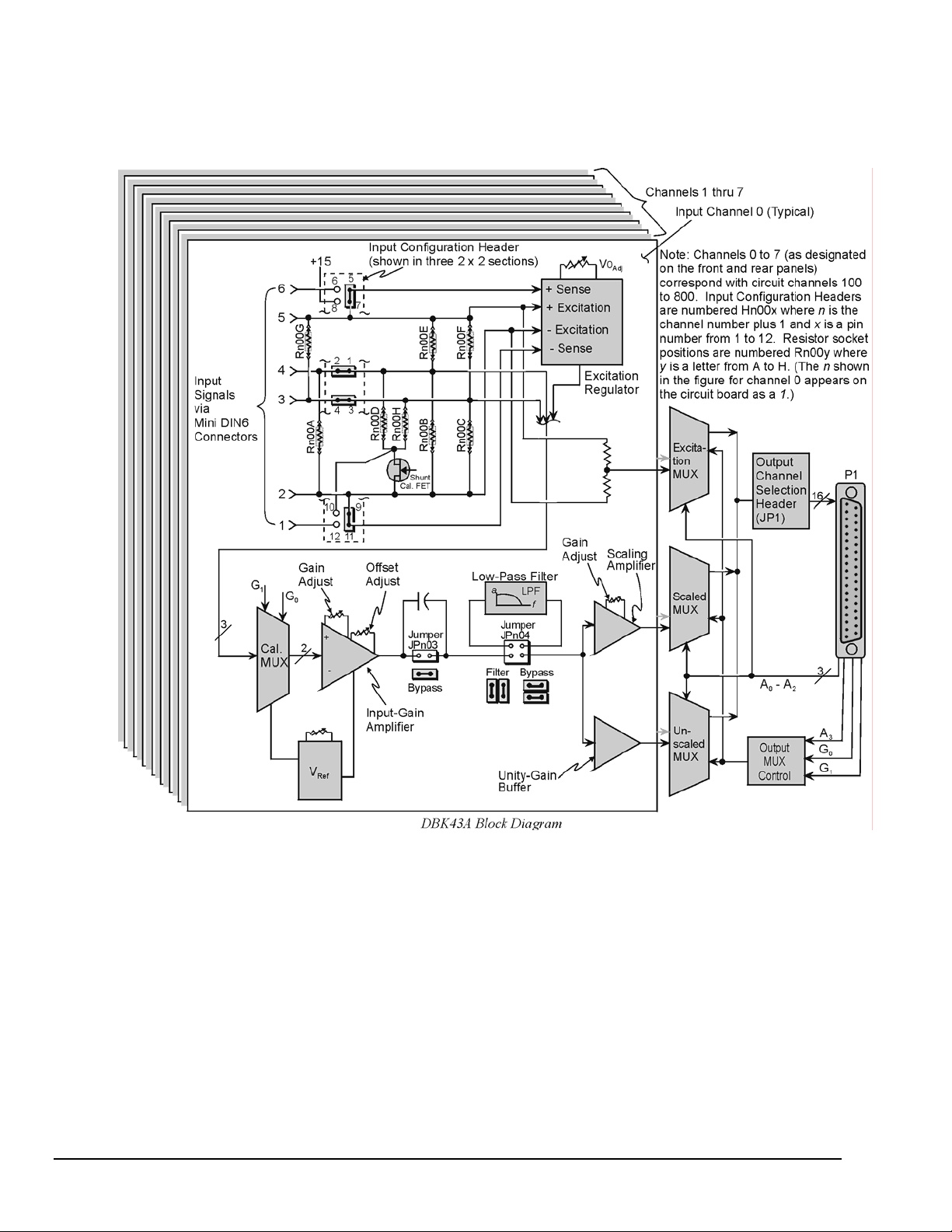
The DBK43A provides an amplifier gain range of ×100 to ×1250 for use with strain gages having
0.4 to 10 mV/V sensitivities. Most strain gages are specified for a full-scale value of weight, force,
tension, pressure, or deflection with an output of mV/V of excitation. For example, a strain gage with a
full-scale rating of 1000 lb of tension might output 2 mV/V of excitation at full load. With an excitation of
10 VDC, 1000 pounds of load would produce an output of 20 mV.
The module’s 0 to 5 VDC offset and output-scaling permit nulling of large quiescent (inactive or
motionless) loads and expansion of the dynamic range for maximum resolution. Typically, the quiescent
output is non-zero. Prior to a force being applied, a mounted strain gage can be in a state of partial
deflection resulting in an output. In the case of a tension gage, this output may be due to the weight of a
hook or empty container.
The DBK43A includes an internal excitation voltage source. The wide-range excitation regulator is
adjustable from 1.5 to 10.5 VDC with a current limit of 50 mA.
DBK43A, pg. 2 877095 DBK Option Cards and Modules
Page 23
Hardware Connection
Power Connection
The DBK43A requires input voltage between +9 and +18 VDC. The DC source should be filtered but not
necessarily regulated—the DBK30A is recommended for portable use. The DBK43A’s isolated DC/DC
converter-based power supply provides all excitation voltages and biasing for its amplifier circuits. Each
of the eight on-board excitation regulators can be adjusted from 1.5 to 10.5 VDC. These outputs have
remote sensing terminals and feature 50 mA current limiting to prevent damage from short-circuit or
overload. The regulators’ wide voltage range can accommodate any resistive or semi-conductive gage
type.
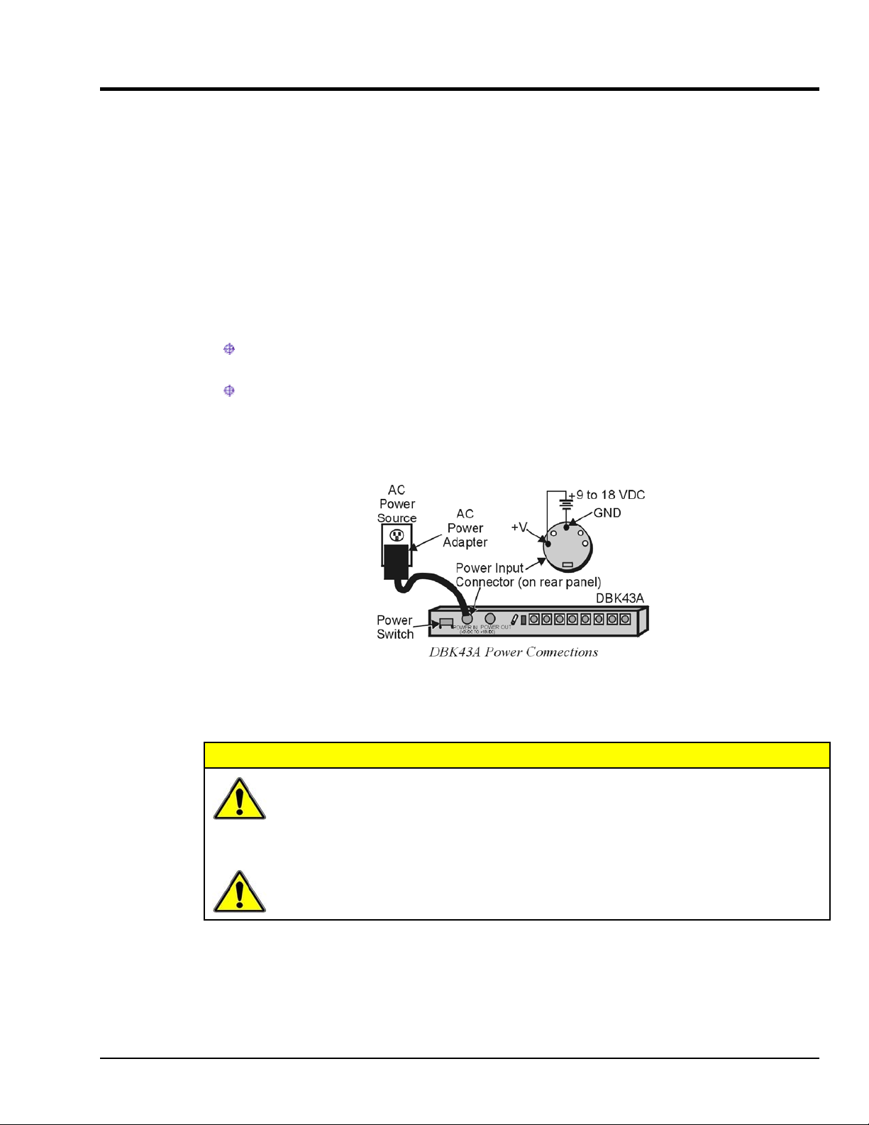
The DBK43A may be powered with the supplied AC adapter that plugs into any standard AC wall outlet or
from any isolated 9-18 VDC source of 16 W (see figure). Before plugging unit in, make sure the power
switch is in the “0” (OFF) position.
If using an AC power adapter, plug it into an AC outlet and attach the low voltage end to the jack
on the DBK43A.
If using another 9 VDC to 18 VDC source, make sure the leads are connected to the proper DIN
terminals.
CAUTION
DBK Option Cards and Module 877095 DBK 43A, pg. 3
POWER IN : The power connectors are rated at 5 amps maximum DC current. The
power supply provided with the DBK43A can power the unit but not any auxiliary
devices. If using the DBK43A’s power supply, do not use the POWER OUT terminal.
If using another power supply to power auxiliary devices from the POWER OUT
terminal, make sure that power supply is current-rated for the units connected (up to 5
amps DC).
POWER OUT : Maximum output current is 3 amps DC. Use a power supply capable of
supplying 5 amps DC at POWER IN.
Page 24
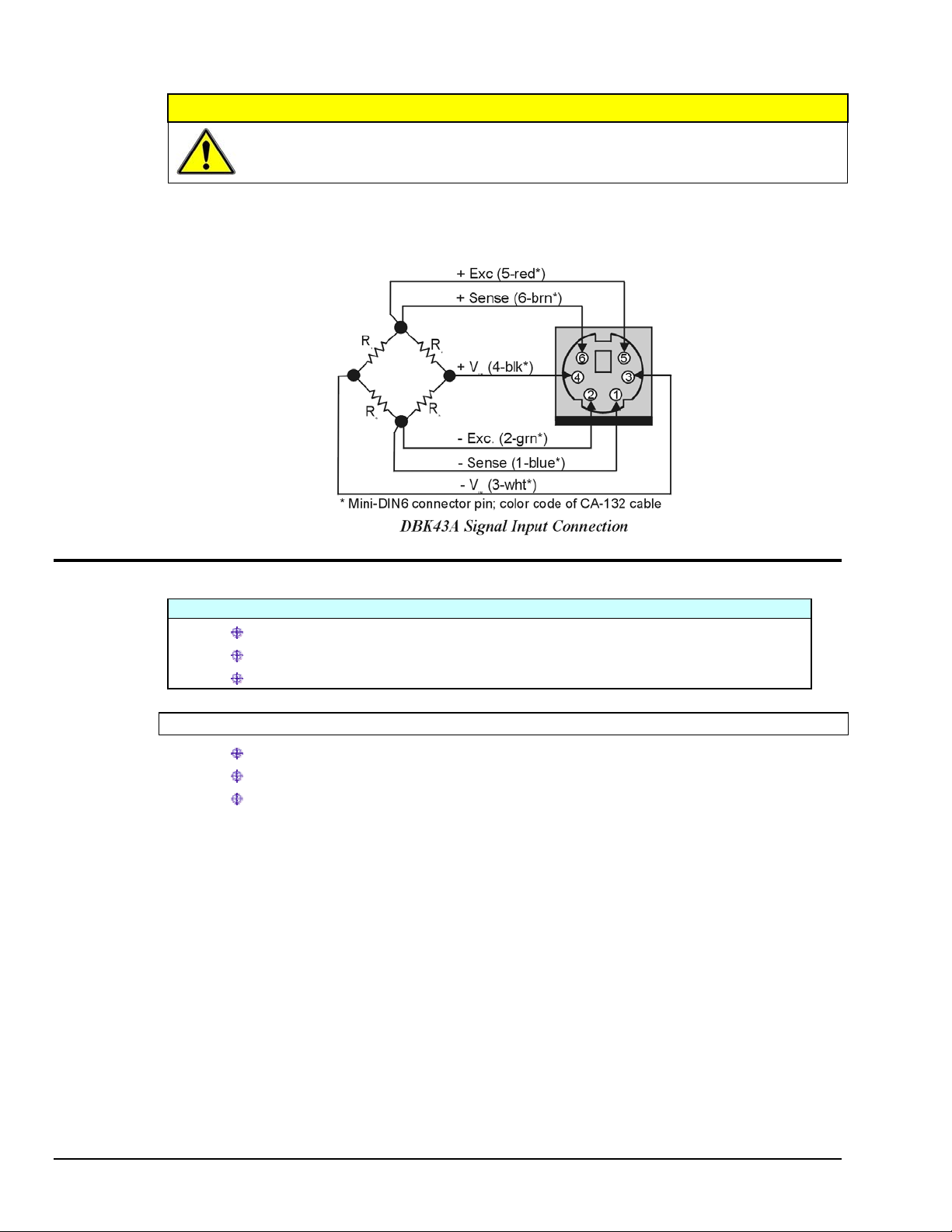
Signal Connection
The following figure shows the 6-pin signal connector (1 of 8) on the back of the DBK43A, and a fullbridge with remote sensing configuration.
CAUTION
The maximum channel signal input from input pin #4 (V+) to pin #3 (V-) is 50 mV.
There is no common-mode isolation between inputs (common-mode voltage between
inputs must be 0 V).
Hardware Configuration
Factory Defaults:
Bridge configuration: Full
Coupling: DC
Low pass filter: Disabled (bypassed); resulting in 3.8 Hz cutoff-frequency
Configuration options on the DBK43A are:
Bridge Applications using various bridge-completion resistors and jumpers
AC Coupling and Low-Pass Filter Options
P1 Output Channel and Card Address Selection
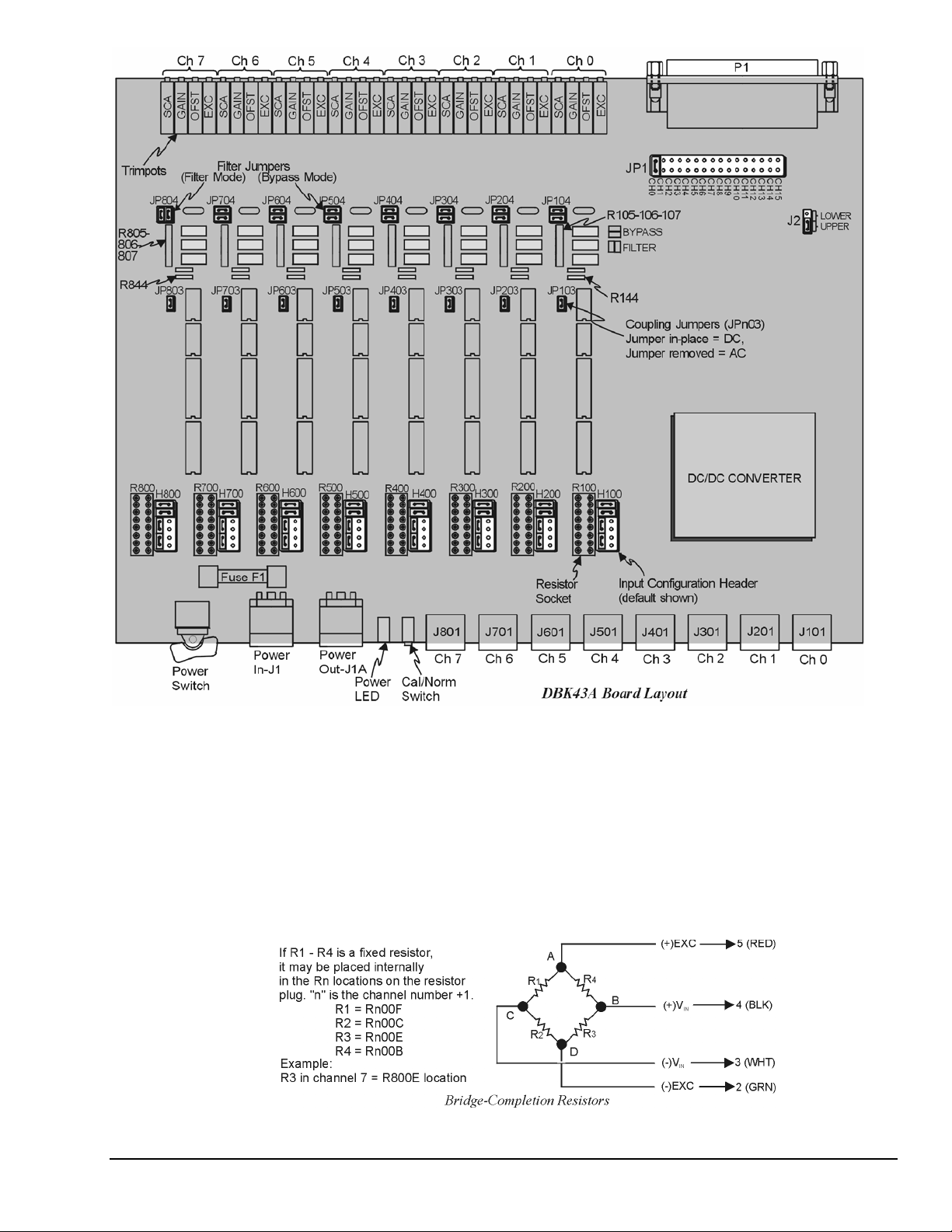
The following board layout can be referred to for jumper, switch, and resistor locations.
DBK43A, pg. 4 877095 DBK Option Cards and Modules
Page 25
Bridge Applications
There are several ways to hook-up strain gages—all are configured into a 4-element bridge (the 4 legs in a
bridge circuit). The quarter-, half- or full- designation for a strain gage refers to how many elements in the
bridge are strain-variable. A quarter bridge has 1 strain-variable element; a half bridge has 2 strainvariable elements; and a full bridge has four strain-variable elements. Each channel of the DBK43A has
locations for bridge-completion resistors when using quarter- and half-bridge strain gages. These resistors
are fixed values necessary to fill out the 4-element bridge configuration.
The following is a standard symbol for a 4-element bridge type strain gage. The figure makes use of
bridge-completion resistor designations for a DBK43A channel.
DBK Option Cards and Module 877095 DBK 43A, pg. 5
Page 26
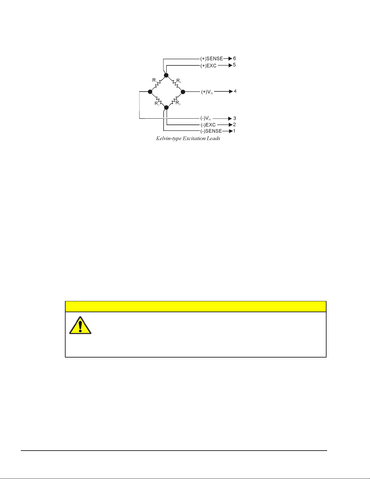
Any or all of the 4 resistive elements may be strain-variable. Where an element is a fixed resistor, the
fixed resistor may be installed in the internal location provided. (The n is the channel number +1; for an
internal resistor on channel 7, the location is R800E.)
Connections are provided for Kelvin-type excitation. The excitation regulators stabilize the voltage at the
points connected to the on-board sampling dividers. Unless you run separate sense leads to the excitation
terminals of the strain gage, the voltage regulation is most accurate at the terminal blocks on the DBK43A.
In a Kelvin-type connection, six wires run to a 4-element strain gage, and the excitation regulation is
optimized at the strain gage rather than at the terminal blocks. This connection works with as little as 10
feet of 22 gauge lead wire if accuracy is critical. (See Full-Bridge with Remote Excitation Sensing
Configuration in full-page figure.)
The Kelvin connection using the remote sensing lines performs best when the entire bridge is localized (no
bridge-completion resistors inside the DBK43A) and all leads are contained in a multi-conductor cable. If
individual wire leads are used, the two sense wires should be tightly twisted to form a pair. Likewise, the
two excitation wires and the two bridge-output wires should be twisted together).
The internal excitation source is attached to a voltage regulator in the DBK43A circuitry. This regulator
provides the excitation to the actual transducer (there is a separate regulator for each transducer, hence 8
regulators per DBK43A). Each regulator has a maximum current of 50 mA. The maximum excitation
voltage that can be provided by the DBK43A excitation regulator is: 0.05 × R (where R = the resistance in
ohms of 1 element in the bridge circuit).
CAUTION
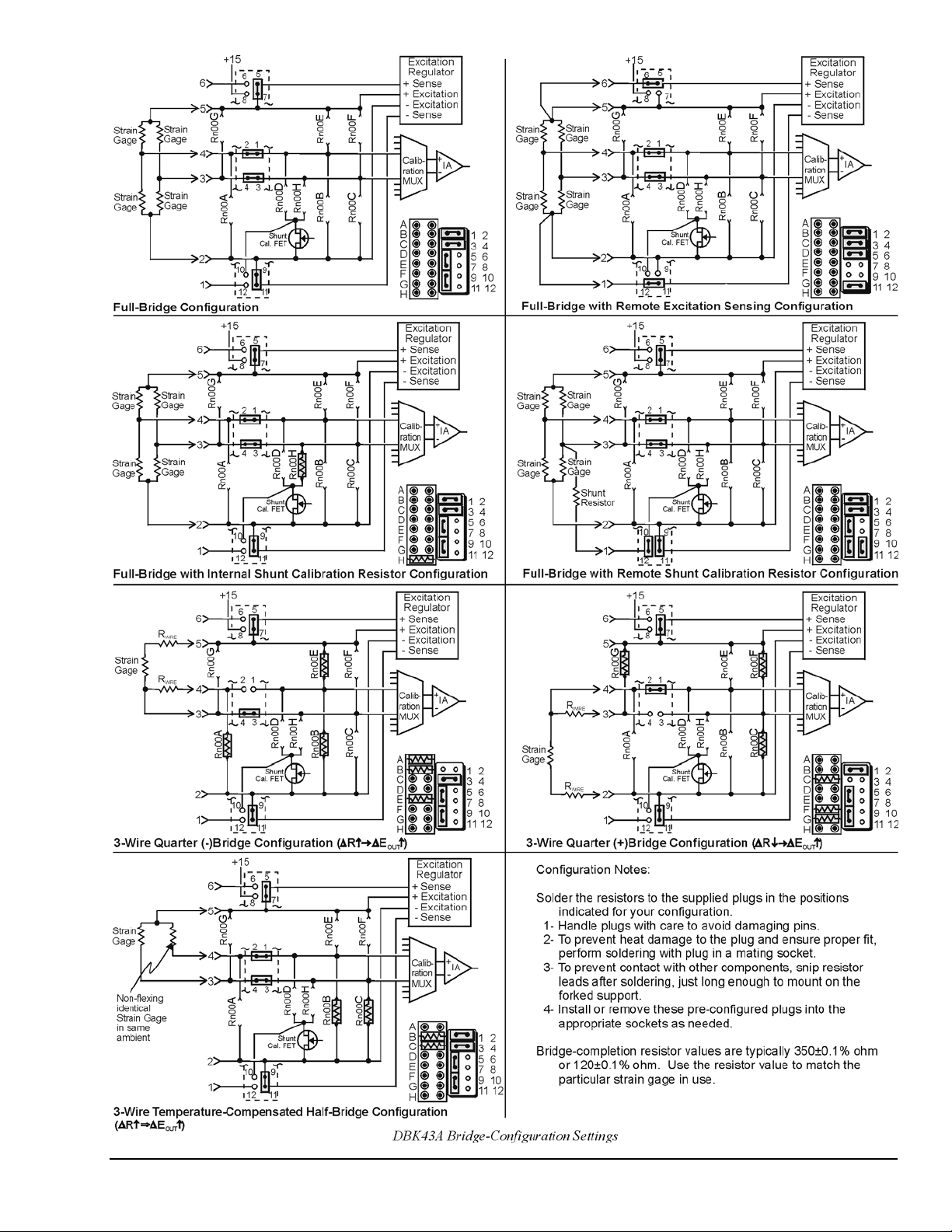
The following full-page figure shows various strain-gage configurations.
Setting the excitation voltage above the maximum voltage allowed can cause the
DBK43A to fail. The maximum allowable excitation voltage is determined by the
following equation.
V
MAX[EXC]
= 0.05 x R
R is the resistance in ohms of 1 element in the bridge circuit.
DBK43A, pg. 6 877095 DBK Option Cards and Modules
Page 27
DBK Option Cards and Module 877095 DBK 43A, pg. 7
Page 28

Input Configuration Headers
Eight 2×6 pin-headers with pin numbers 1 to 12 are on the board, 1 for each channel designated H100
(channel 0) to H800 (channel 7). The user can position jumpers on this header to configure inputs from a
variety of bridge types.
Jumping header pins 1-to-2 and 3-to-4 connects the +Vin and -Vin to the calibration MUX for
different bridge configurations.
Jumping pins 5-to-7 and 9-to-11 allows internal sense regulation of the excitation regulator.
Jumping pins 5-to-6 and 11-to-12 allows for remote excitation sensing.
Jumping pin 10-to-12 allows the use of a remote shunt-calibration resistor.
See previous figure for header configurations that correspond with different bridge-wiring schemes.
Resistor Sockets and Adapter Plugs
Eight 2×8 resistor sockets with rows numbered A to H are on the board; 1 socket
for each channel and designated R100 (channel 0) to R800 (channel 7). An
adapter plug for soldering resistors is included for each channel; user-soldered
plugs facilitate changing configurations as needed.
Bridge-completion resistors include: Rn00B, Rn00C, Rn00E, and Rn00F.
Resistors Rn00A and Rn00G are used to complete 3-wire strain-gage
configurations.
Rn00D and Rn00H are internal shunt resistors from +V in and -V in
respectively to -excitation.
Just inserting resistors into the socket makes an unreliable connection and is not
recommended. To achieve a reliable connection, solder resistors to the adapter
plug to match the proper row as shown in the previous figure, DBK43A Bridge-
Configuration Settings. Soldering should be done with the plug inserted into the
resistor socket; otherwise, heat from soldering can distort the shape of the plug.
After soldering, the resistor leads should be snipped off close to the support to
prevent contact with other components.
Handle the adaptor plugs with care to prevent pin damage.
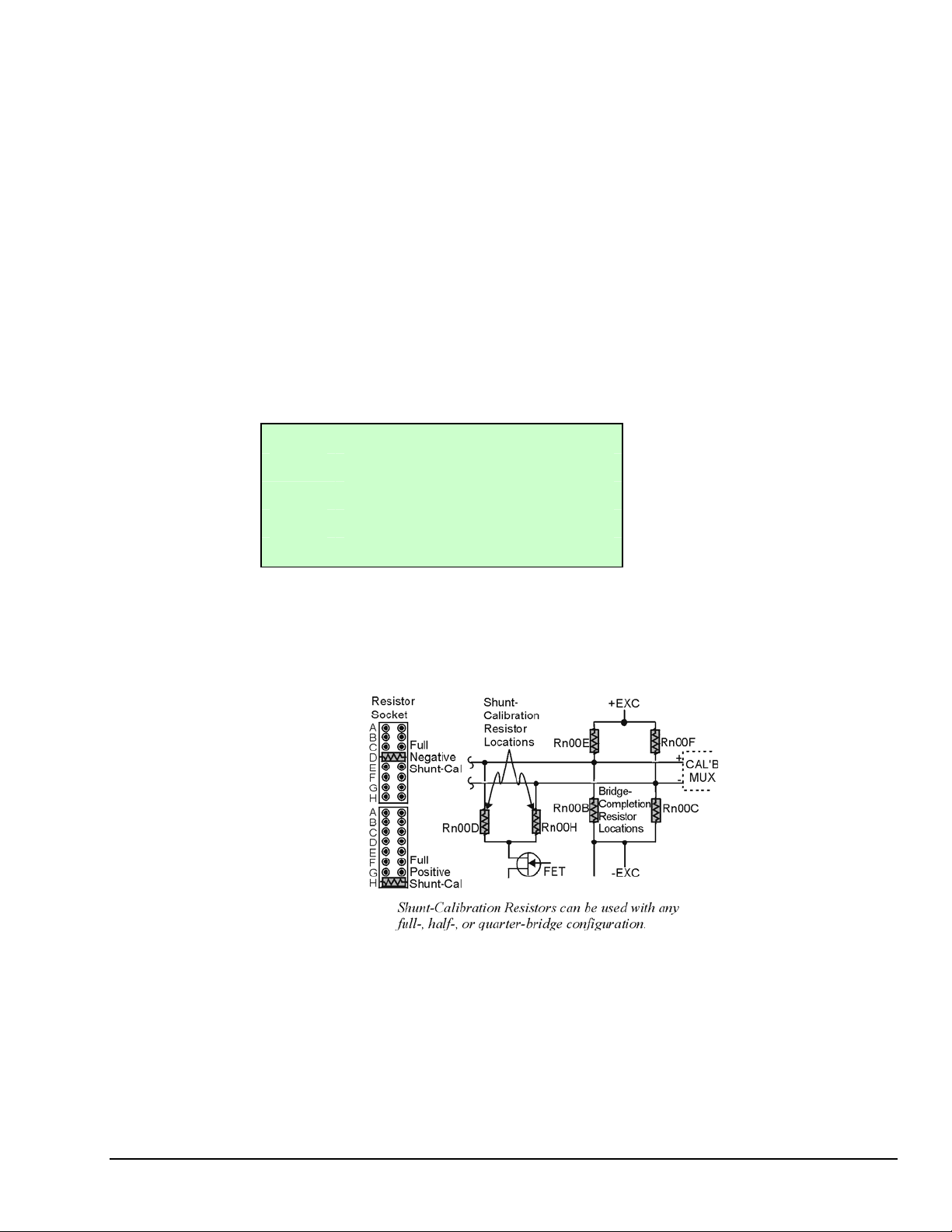
Shunt-Calibration Resistors
The DBK43A provides physical locations for internal shunt-calibration resistors. Each channel has resistor
locations that can be shunted across one or the other of the lower bridge arms by a hardware and softwareaccessible solid state switch (FET transistor) to create a repeatable bridge imbalance with a precision
resistor.
For any balanced bridge, a resistance value can be applied in parallel with one of the four bridge elements
to create a predictable imbalance and output voltage. For example, a 350Ω 2mV/V strain gage will deliver
full output if one arm drops by 0.8% (about 2.80Ω) to 347.2Ω. A 43.4 KΩ resistance shunted across one
or the other lower bridge elements will result in full-positive (Rn00H) or full-negative (Rn00D) output.
For best results, Rn00H and Rn00D should be across the strain element when it is switched in.
DBK43A, pg. 8 877095 DBK Option Cards and Modules
Page 29
A formula used to calculate the shunt-cal resistance value is:
R
Shunt
Where:
= [R
R
Shunt
R
Gage
Gage / FG
= the shunt calibration resistor value
= the resistance of the gage
(ε) ] - R
Gage
FG = the gage factor
ε = the strain value of the gage
Example:
An engineer wants to know the shunt calibration resistor value for a strain gage with the following
parameters.
resistance: 120 Ω
gage factor: 2.0
strain: 5000 micro-strain, i.e., 5000 x 10
Plugging the values into the equation, we get:
R
Shunt
In all cases, the resistance of the solid-state switch will be negligible when compared to the shunt
resistance. Changing the CAL/NORM switch (on the rear panel) to the CAL position while reading the
bridge will activate the shunt-calibration resistors. After reading the offset, return the switch to the NORM
position for normal bridge readings.
= [R
Gage / FG
(ε) ] - R
Gage
= [120 / 2.0(5000 x 10-6)] - 120
= [120 / .01] – 120
= 12000 – 120
= 11,880 Ω
-6
DBK Option Cards and Module 877095 DBK 43A, pg. 9
Page 30
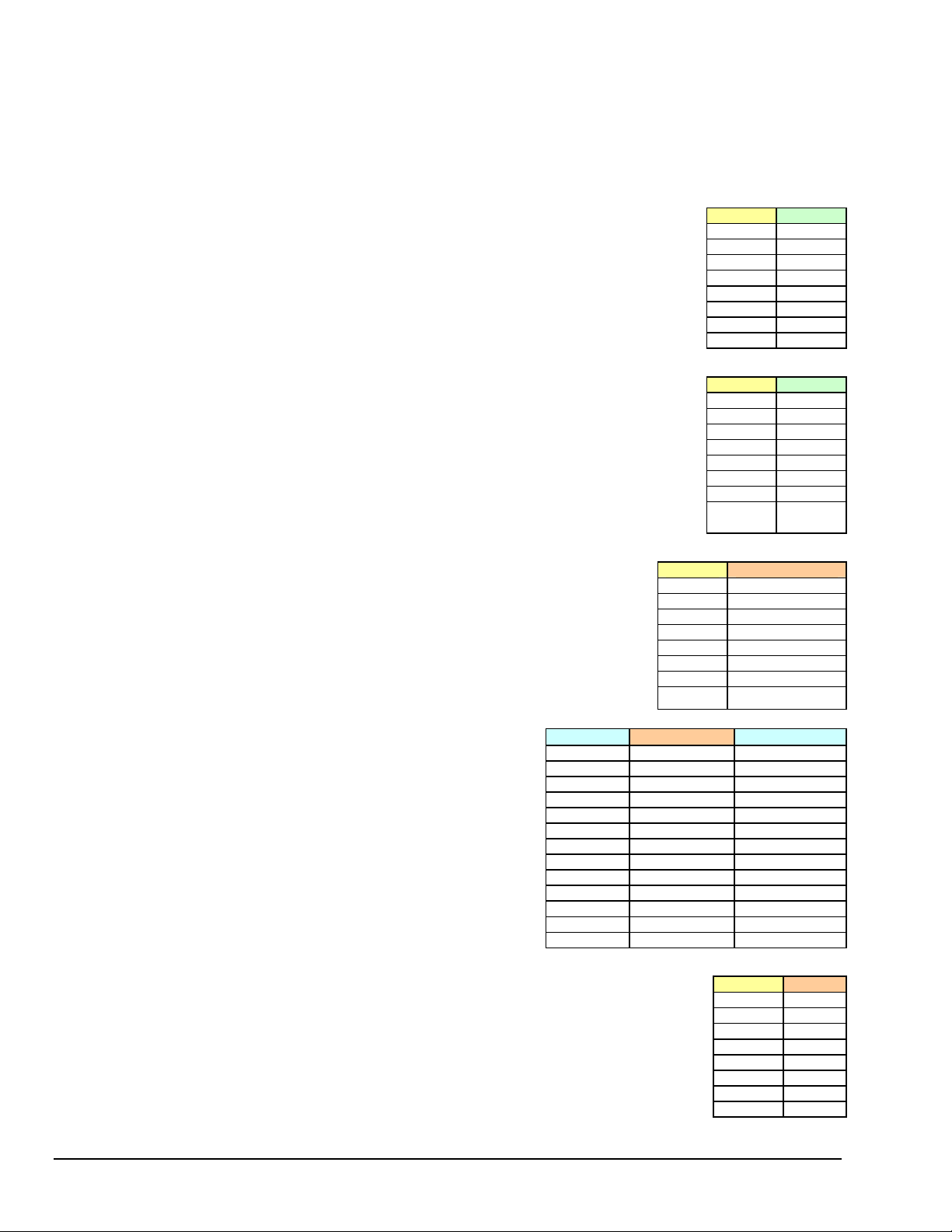
AC Coupling and Low-Pass Filter Options
Per channel, the DBK43A accommodates coupling and low-pass filter options including:
• AC coupling, or DC coupling
• Using or bypassing the filter
• Choice of the filter’s corner frequency via a SIP resistor network
• Filter gain (default of ×2 can be changed to ×1).
The AC coupling, or DC coupling choice on each channel is set by the presence or
absence of shunt jumpers on 2-pin headers. If the shunt jumper is in place, the
coupling is DC. If the shunt jumper is absent, the coupling is AC. See table for
channels and corresponding headers.
The choice of using or bypassing the low-pass filter for each channel is made by the
orientation of two shunt jumpers on a 2×2 pin header. When the shunt jumpers are
oriented horizontally (like the “bypass” symbol on the circuit board) the filter is
bypassed. When the shunt jumpers are oriented vertically (like the “filter” symbol),
the filter is in the signal path.
Channel Header
0 JP103
1 JP203
2 JP303
3 JP403
4 JP503
5 JP603
6 JP703
7 JP803
Channel Header
0 JP104
1 JP204
2 JP304
3 JP404
4 JP504
5 JP604
6 JP704
7 JP804
The corner frequency of a low-pass filter is determined by three resistor
values in each filter circuit. The resistors are listed in the following table.
These resistor locations have been physically arranged to allow the use of a
6-pin SIP network as a convenient means of changing all 3 resistors. The
machined-pin socket will also allow you to insert individual resistors.
Channel Resistors
0 R105-R106-R107
1 R205-R206-R207
2 R305-R306-R307
3 R405-R406-R407
4 R505-R506-R507
5 R605-R606-R607
6 R705-R706-R707
7 R805-R806-R807
The next table is a list of some common frequencies, the
nominal resistance value, and a Bourns part number for a
suitable network.
Frequency
133kHz 10 4606X-102-100
66.7kHz 20 4606X-102-200
26.6kHz 50 4606X-102-500
13.3kHz 100 4606X-102-101
6.67kHz 200 4606X-102-201
2.66kHz 500 4606X-102-501
1.33kHz 1K 4606X-102-102
667Hz 2K 4606X-102-202
266Hz 5K 4606X-102-502
133Hz 10K 4606X-102-103
66.7Hz 20K 4606X-102-203
26.6Hz 50K 4606X-102-503
13.3Hz 100K 4606X-102-104
Resistance (Ω)
Bourns P/N
The active low-pass filters on the DBK43A have a gain of ×2. This gain can be
factored into the setup calculations, or the filter gain can be changed to ×1. To
change the gain to ×1 (unity) for the corresponding channels, de-solder (or snip leads)
and remove the resistors shown in the table.
Note: The default ×2 gain option meets the needs of most applications.
Channel R (10K)
0 R144
1 R244
2 R344
3 R444
4 R544
5 R644
6 R744
7 R844
DBK43A, pg. 10 916894 DBK Option Cards and Modules
Page 31
P1 Output Channel and Card Address Selection
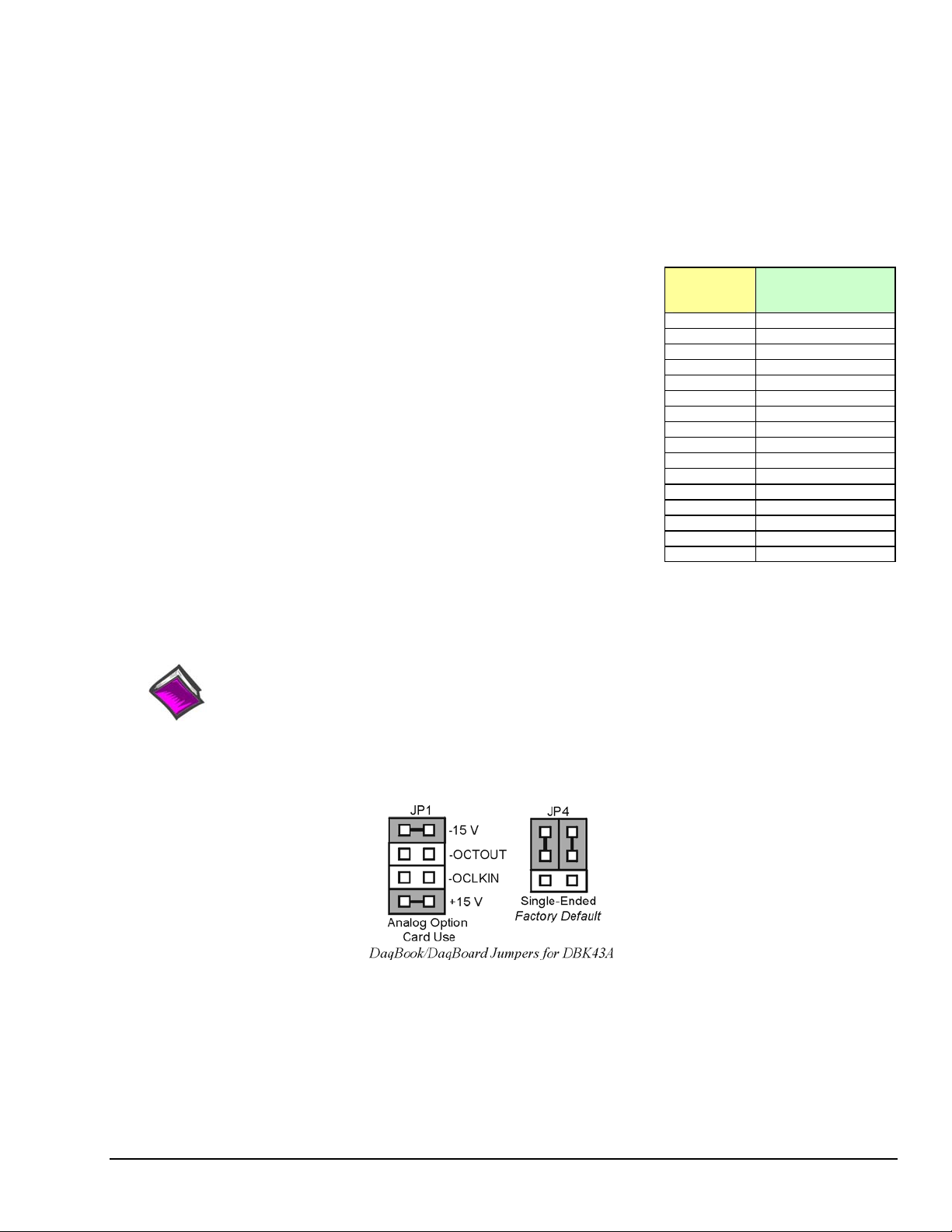
All 8 channels on the DBK43A are multiplexed into 1 of the LogBook or Daq Device base channels
(0 to 15). The base channel (that the DBK43A is multiplexed into) is set by the shunt jumper on the 16×2
header designated JP1.
Each base channel can have up to 16 expansion channels multiplexed into it. Since the DBK43A
represents 8 expansion channels, 2 DBK43A modules can be multiplexed into each LogBook base channel.
To distinguish channels, there is a 3-pole header (designated J2) with a shunt jumper that can be placed in
1 of 2 positions for either LOWER (0 to 7) or UPPER (8 to 15) expansion channels.
With the LogBook or Daq device’s 16 base channels, up to 32
DBK43As can be used for a maximum of 256 channels. These
channels are identified differently in the API for custom
programming and in DaqView and GageCal.
For the API, the base channels are designated 0 to 15; and expansion
channels are designated 16 to 271. Channel 16 is the first channel
on the first expansion board (for DBK43A, channel 0 on lower
DBK43A with JP1 set to CH0) and channel 271 is the last channel
on the last expansion board (for DBK43A, channel 7 on upper
DBK43A with JP1 set to CH15). The table shows the base channel
and the first expansion channel number (N) associated with that
particular base channel. To calculate the actual input channel, add
“N” to “n”. (If J2 is set to LOWER, the n-values for input channels
0 to 7 range from n = 0 to n = 7; if J2 is set to UPPER, the n-values
range from
n = 8 to n = 15.) This expansion channel number is also needed
when writing a program to read from that particular channel.
Daq Device
Base
Channel
0 16
1 32
2 48
3 64
4 80
5 96
6 112
7 128
8 144
9 160
10 176
11 192
12 208
13 224
14 240
15 256
First Expansion
Channel Number (N)
For DaqView , LogView and GageCal, these same 256 channels are identified from ch0-0-0 to ch15-2-7.
The first field (0 to 15) is the base channel; the second field is the lower (1) or upper (2) sub-channel
selected on J2; and the third field (0 to 7) is the 8 channels on a single DBK43A.
Reference Note:
For more information on channel multiplexing, refer to Chapter 1, Signal Management.
DaqBook/100 Series & /200 Series and DaqBoard [ISA type] Configuration
Use of the DBK43A requires setting jumpers in DaqBooks/100 Series & /200 Series devices
and ISA-type DaqBoards.
1. If not using auxiliary power, place the JP1 jumper in the expanded analog mode.
Note: This default position is necessary to power the interface circuitry of the DBK43A via the internal
±15 VDC power supply. If using auxiliary power (DBK32A or DBK33), you must remove both
JP1 jumpers. Refer to Power Management in the DBK Basics section [at the front of the manual]
and to the DBK32A and DBK33 document modules as needed.
DBK Option Cards and Module 877095 DBK 43A, pg. 11
Page 32
2. For DaqBook/100, DaqBook/112 and DaqBook/120, place the JP4 jumper in single-ended mode
Note: To use a DBK43A with a Daq PC-Card, you must an appropriate power module must be used.
DaqBook/2000 Series and DaqBoard/2000 Series Configuration
No Jumper configurations are required for these /2000 series devices.
Hardware Adjustment
Bridge circuit transducers are used for many different applications, and the DBK43A is flexible enough to
support most of them. Each DBK43A channel circuit has an excitation regulator, a high gain (100-1250)
input amplifier with offset adjustment, a low-pass filter, a scaling (1-10) amplifier, and a calibration
multiplexer.
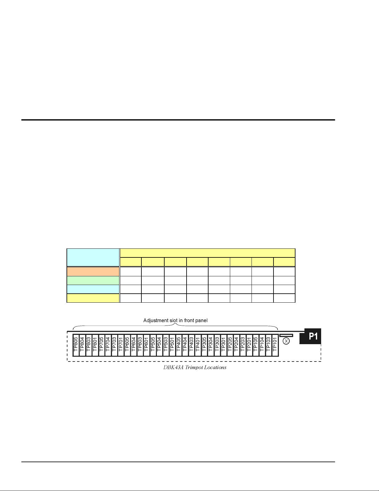
Trimpots
The DBK43A’s front panel has a slot to allow access to 4 potentiometers to trim (adjust) the accuracy for
each channel circuit. The trimpots are labeled to represent the following adjustments:
EXC for adjusting the excitation voltage to the transducer
Trimpot
EXC
GAIN
OFFSET
SCALE
The figure shows trimpot locations.
CAL/NORM Switch
The CAL/NORM switch is located between the CH7 input and the power LED on the rear panel.
GAIN for setting the gain of the input amplifier
OFFSET for adjusting the circuit offset for quiescent loads or bridge imbalance
SCALE for setting the gain of the scaling amplifier
Channel Number
CH0 CH1 CH2 CH3 CH4 CH5 CH6 CH7
TP101 TP201 TP301 TP401 TP501 TP601 TP701 TP801
TP104 TP204 TP304 TP404 TP504 TP604 TP704 TP804
TP103 TP203 TP303 TP403 TP503 TP603 TP703 TP803
TP105 TP205 TP305 TP405 TP505 TP605 TP705 TP805
• In the NORM position, the function of the pr imary data acqu isition is identical with that of the
DBK43.
• In the CAL position, the shunt calibration offset and the excitation voltage can be read depending on
the software function control described next.
DBK43A, pg. 12 877095 DBK Option Cards and Modules
Page 33
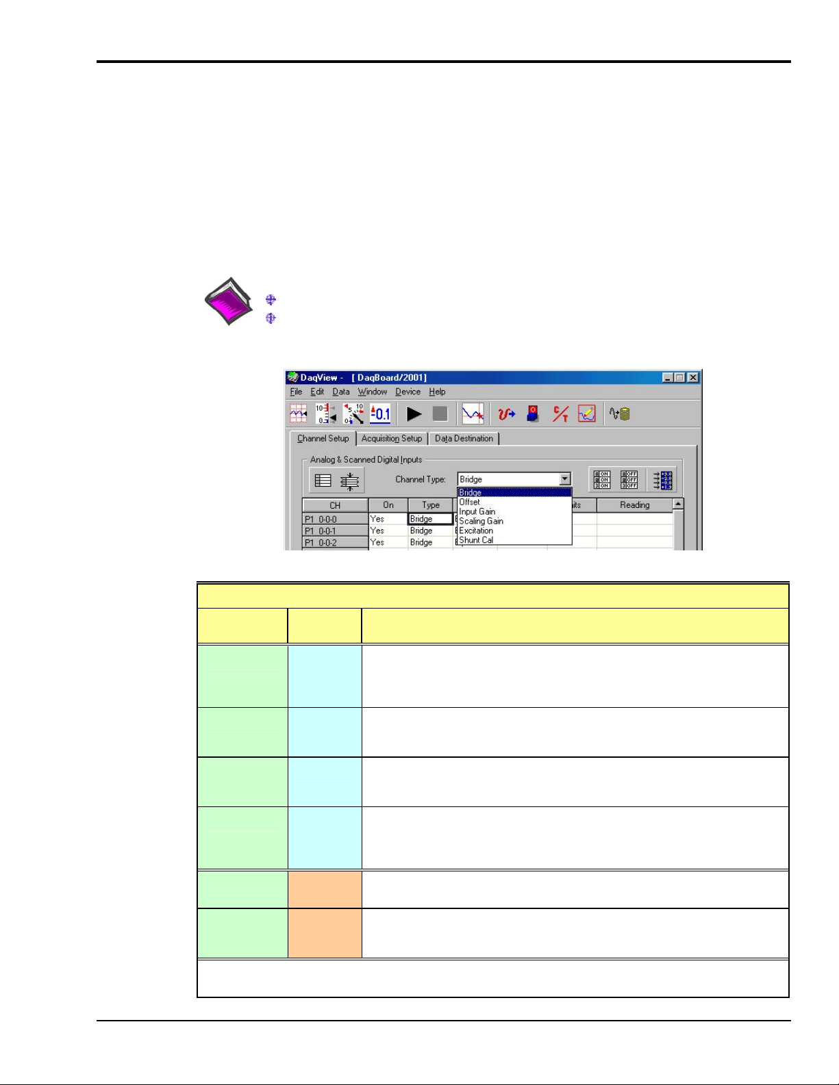
Software-Controlled Setup
Proper setup includes the use of software to control the calibration multiplexer in each circuit. The
calibration multiplexer is used to switch the bridge circuit out and ap ply internal reference voltages to the
input for use in the DBK43A setup. The calibration multiplexer also allows the recording of the individual
adjustments.
The next two tables identify functions available through DaqView and LogView, respectively. Note that
DaqView uses the term “Channel Type;” and LogView uses the term “Mode.” The tables include
equations in which “V
device, i.e., a LogBook, DaqBook, DaqBoard, or other Daq device.
OUT
” (voltage out) represents the voltage recorded by the primary data acquisition
Selecting Channel Types in DaqView
Channel Type CAL/NORM
Bridge
Offset
Input Gain
Scaling Gain
Excitation
Shunt Cal
1
The physical CAL/NORM Switch [on the DBK43A Module] is located next to the Power LED.
* In the equations, the asterisk indicates the conditional clause, “if the filter is enabled.”
Reference Notes:
LogView user’s refer to Selecting Channel Modes in LogView on page DBK43A-14.
Typical setup steps with embedded examples begin on page DBK43A-15. The steps
can be used for LogBook and Daq device applications.
Selecting Channel Type for DBK43A In DaqView
Using DBK43A Channel Types in DaqView
Function and Associated V
1
Switch
NORM
NORM
NORM
NORM
CAL
CAL
Sets the channel to read the value of the bridge circuit with all gains and offsets in
effect. This is the normal operation.
Vout = (Scaling Gain)(Filter Gain*)[(InputGain)(bridge circuit voltage) - offset
voltage]
Applies a grounded input to the channel. Sets the channel to read the circuit offset
voltage multiplied by the input amplifier and the low-pass filter gain.
Vout = (Filter Gain*)(Input Gain)(-offset voltage)
Applies 5 mV to the input channel. Sets the channel to read the voltage out of the
circuit through the input gain amplifier and the low-pass filter [if enabled].
Vout = (Filter Gain*)(Input Gain)(5 mV) - offset voltage
Applies 5 mV to the input channel. Sets the channel to read the voltage out of the
circuit through the input gain amplifier, the low-pass filter [if enabled], and the
scaling gain amplifier.
Vout = Filter Gain*(Scaling Gain[(Input Gain)(5 mV) - offset voltage])
Sets excitation.
Vout = (Excitation Voltage)
Activates shunt-cal resistors.
Vout = (Scaling Gain)(Filter Gain*)[(Input Gain)( bridge circuit voltage with shunt) -
offset voltage]
Equation
OUT
DBK Option Cards and Module 877095 DBK 43A, pg. 13
Page 34
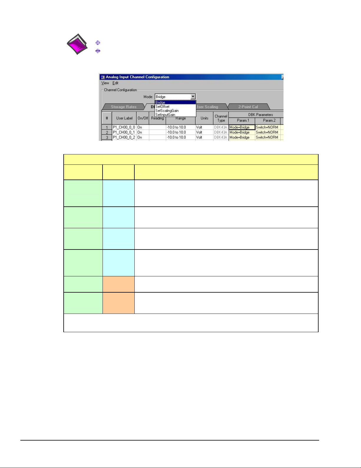
Selecting Channel Modes in LogView
Mode
Bridge
SetOffset
SetInputGain
SetScaling
Gain
Excitation
Shunt Cal
1
The CAL/NORM Switch is located on the DBK43A Module, next to the Power LED.
* In the equations, the asterisk indicates the conditional clause, “if the filter is enabled.”
Reference Notes:
DaqView users refer to Selecting Channel Types in DaqView on page DBK43A-13.
Typical setup steps with embedded examples begin on page DBK43A-15. The steps
can be used for LogBook and Daq device applications.
Selecting Channel Mode for DBK43A In LogView
Using DBK43A Channel Modes in LogView
CAL/NORM
Switch
NORM
NORM
NORM
NORM
CAL
CAL
Function and Associated V
1
Sets the channel to read the value of the bridge circuit with all gains and offsets in
effect. This is the normal operation.
Vout = (Scaling Gain)(Filter Gain*)[(InputGain)(bridge circuit voltage)
- offset voltage]
Applies a grounded input to the channel. Sets the channel to read the circuit offset
voltage multiplied by the input amplifier and the low-pass filter gain.
Vout = (Filter Gain*)(Input Gain) - offset voltage
Applies 5 mV to the input channel. Sets the channel to read the voltage out of the
circuit through the input gain amplifier and the low-pass filter [if enabled].
Vout = (Filter Gain*)(Input Gain)(5 mV) - offset voltage
Applies 5 mV to the input channel. Sets the channel to read the voltage out of the
circuit through the input gain amplifier, the low-pass filter [if enabled], and the
scaling gain amplifier.
Vout = Filter Gain*(Scaling Gain[(Input Gain)(5 mV) - offset voltage])
Sets excitation.
Vout = (Excitation Voltage)
Activates shunt-cal resistors.
Vout = (Scaling Gain)(Filter Gain*)[(Input Gain)( bridge circuit voltage with shunt)
- offset voltage]
Equation
OUT
DBK43A, pg. 14 877095 DBK Option Cards and Modules
Page 35

A Typical Setup Procedure, with Embedded Examples
Reference Notes:
Prior to using DBK43A with DaqView you must select the DBK43A from DaqView’s
Configure Hardware Settings screen. If needed, refer to Chapter 3, DBK Setup in
DaqView.
Prior to using DBK43A with LogView you must select the DBK43A from LogView’s
Hardware Configuration screen. If needed, refer to Chapter 4, DBK Setup in LogView.
The board layout on page DBK43A-5 can be referred to for jumper locations, jumper
setting orientations, and trimpot locations.
For Calibration of DBK43A – DaqView users should refer to the GageCal segment
beginning on page DBK43A-19 . LogView users should refer to the section titled
Calibrating DBK16 and DBK43A for LogBook Applications, beginning on page
DBK43A-23.
1. Verify that the low-pass filters are set to BYPASS. The filters are set via jumpers JPn04 where n is
the channel number (1 through 8); for example, JP104 sets the filter for channel 1, and JP804 sets the
filter for channel 8.
Note:
If you plan to use filters during your acquisition, you should still select BYPASS at this
point. Enabling the filters comes into play later in the procedure. However, if you do plan
to enable filters, note the gain in the filter stage (default ×2, or ×1 with resistor removed)
and allow for it in your setup.
2. Coupling is set via jumpers JPn03 where n is the channel number (1 through 8). Verify that the
“Coupling” jumpers are installed. When installed, the channels are set for DC coupling.
Note:
If you plan to use AC Coupling during your acquisition, you should still select DC
Coupling at this point. Selecting AC Coupling comes into play later in the procedure.
3. Determine the excitation for the transducer. This is based on the transducer specifications and from
the current limitations of the DBK43A excitation regulator.
4. Determine the maximum voltage that can result from the transducer for a strain gage or for a load
cell. The values can be calculated as follows:
Strain Gage Example
Most strain gages come with Gage Factors (GF). To calculate the approximate output of the bridge
circuit with a typical strain value, use the formula:
()Excitation Voltage)(Gage Factor)(Strain in strain units
4
*Bridge circuit output voltage
=
In this strain gage example, lets assume the following:
• We have a 120 ohm strain gage.
• The gage factor is 2.1.
• The excitation voltage is 5 V. This is due to the current limitation of the ex citation regulator
on the DBK43A [note that the excitation voltage must be less than 6 V]
• We are measuring 4000 micro-strain
By applying these values to the preceding equation we find that the bridge output voltage is 10.5 mV.
-6
Bridge output voltage for 4000 microstrain =
(5)(2.1)(4000 10 )
×
=
10.5 mV
4
*linear estimate (some strain gages are not linear); refer to strain-gage theory for more information.
DBK Option Cards and Module 877095 DBK 43A, pg. 15
Page 36
Load Cell Example
Load cells come with a mV/V specification; for each volt of excitation at maximum load, the load
cell will output a specific millivolt level. The following equation applies:
Load Cell Output Voltage = (Load
Applied
/Load
)(Excitation Voltage)(Load Cell Rating)
Rated
For this example, lets assume the following:
• We have a 350 ohm, 3000 pound load cell.
• The load cell is rated at 2.05 mV/V
• We are using an excitation of 10 V
By applying these values to the preceding equation we find that the Load Cell Output Voltage
is 20.5 mV.
Load Cell Output Voltage = (3000/3000)(10)(2.05×10
-3
) = 20.5 mV
For 1000 pounds applied load, the Load Cell Output Voltage would be one third of the 20.5 mV
value, i.e., 20.5 mV/3 = 6.833 mV. If we used the entire equation we would see:
-3
Load Cell Output Voltage = (1000/3000)(10)(2.05×10
) = 6.833 mV
Now that we know our sensor’s full-scale voltage, we can calculate the DBK43A’s voltage gain.
The proper voltage gain allows the full-scale sensor output to correspond to the full-scale input of the
data acquisition device. Full-scale device inputs are:
-5 to +5 V for DaqBook and DaqBoard [ISA type] in bipolar mode
0 to +10 V for DaqBook, DaqBoard [ISA type], and DaqBoard/2000 Series
in unipolar mode
-10 to +10 V for DaqBoard/2000 Series in bipolar mode and for Daq PC-Card
-10 to +10V for LogBooks in bipolar mode
0 to +20 V for LogBooks in unipolar mode
5. Calculate the channel total gain based on the full-scale LogBook or Daq device.
The following equation is used to calculate DBK43A total gain.
Gain
= (Sensor Output Voltage
TOTAL
FULL-SCALE
– Voltage
) / Strain or Load Voltage
OFFSET
OUTPUT
In this example we will use:
• a full-scale sensor output voltage of +5 V [for a DaqBook in bipolar mode].
• a 0.5 V offset (from full-scale) to prevent saturation
• the 10.5 mV Bridge Output Voltage [for 4000 microstrain] from Example 1.
Using the gain equation we get:
Gain
= (5.0 V – 0.5 V) / 10.5 mV = 4.5 V / 0.0105 V = 428.6
TOTAL
6. Determine how the total gain will be distributed between the input amplifier gain, filter gain, and
scaling amplifier gain.
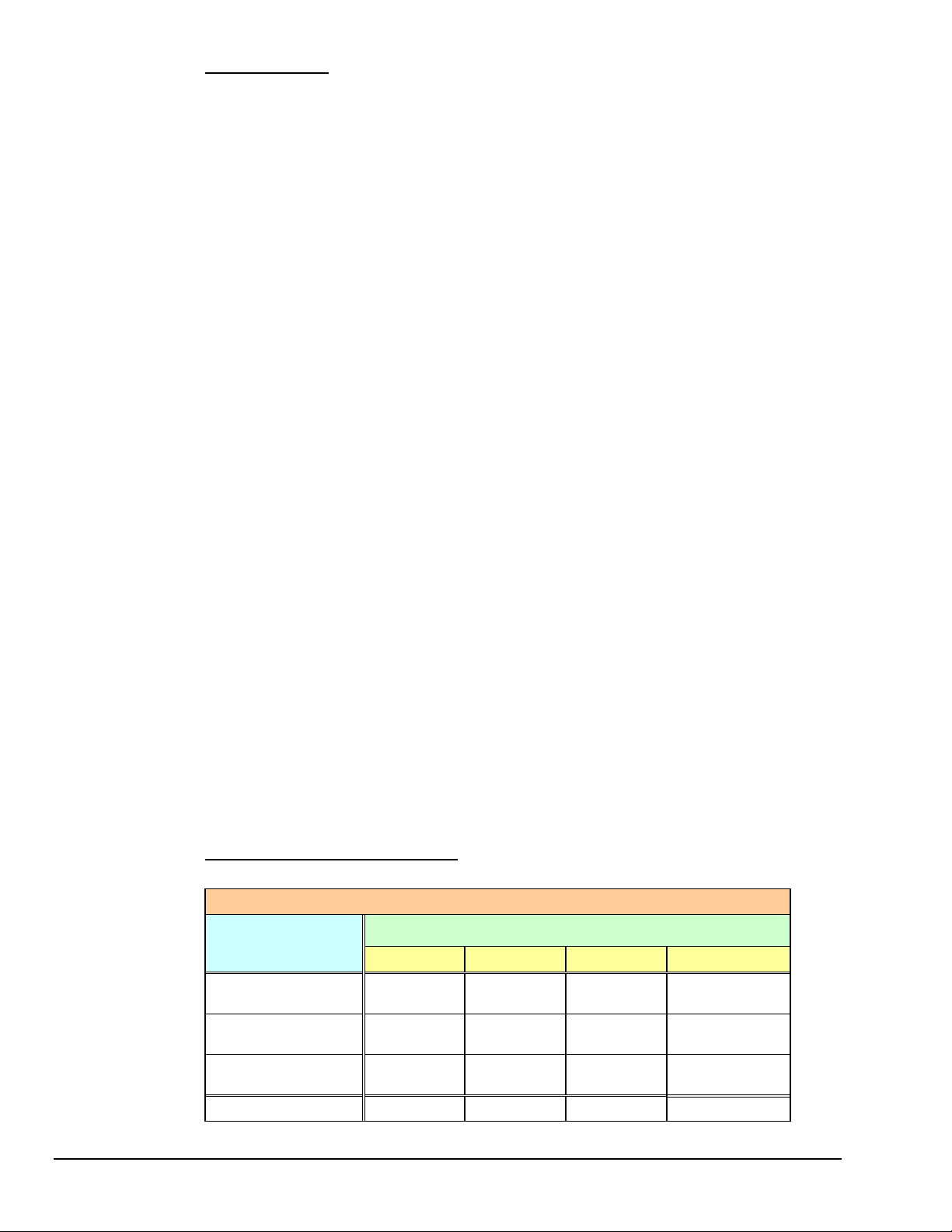
An Example of Total Gain Distribution: If we round the gain of x428.6 [calculated in the previous
step] down to ×420, then the gain distributions indicated by the following table are possible.
Gain Distribution Options for a Total Gain of x420
Gain Stage &
Associated Range
Input Gain
x100 to x1250
Filter Gain
x1 or x2
Scaling Gain
x1 to x10
Total Gain
Option A Option B Option C Option D
×420 ×100 ×240 ×300
Disabled ×2 ×1 Disabled
×1 ×2.1 ×1.75 ×1.4
×420 ×420 ×420 ×420
Possible Gain Distributions
DBK43A, pg. 16 877095 DBK Option Cards and Modules
Page 37
After we decide on a distribution option, the sensor can be hooked up to the DBK43A, the bridge
completion resistors can be installed, the excitation voltage set, followed by setting the gains. In this
example we will be using DaqView. Steps for other programs will be similar.
7. Connect the transducer to the DBK43A according to the figures in the Signal Connection (page 4)
and Bridge Applications (page 5). Install the appropriate bridge-completion resistors if applicable.
8. Adjust the Excitation voltage.
Note: For DaqView versions 5.05 and higher the reading will already be correctly scaled.
(a) Set the DBK43A’s CAL/NORM switch to “CAL.” In addition, LogView users set the
software CAL/NORM switch, in Hardware Configuration, to “CAL.”
(b) Select “Excitation” for the Channel Type.
(c) With the Reading column enabled, set the excitation voltage for the transd ucer by adjusting
the trimpot labeled EXC. Note that each of the eight channels has a channel-specific
trimpot for excitation.
(d) After the excitation voltage is set, stop the Readings.
(e) Return the CAL/NORM switch to the NORM position. In addition, LogView users set the
software CAL/NORM switch to “NORM.”
9. Adjust the Offset.
(a) Verify that the DBK43 A ’s CAL/NORM switch is in the NORM position. In addition,
LogView users verify that the software CAL/NORM switch is selected to “NORM.”
(b) DaqView user’s: select “Offset” for the Channel Type.
LogView users: select “SetOffset” for the Mode.
(c) With the Reading column enabled, adjust the OFFSET trimpot (OFST) to obtain a channel
reading of 0.00 volts. This removes all offset from the DBK43A channel circuit. Note that
each of the eight channels has a designated, channel-specific, trimpot for offset.
(d) After the Offset is adjusted to 0.00, stop the Readings.
10. Adjust the Input Gain.
(a) DaqView users: select “Input Gain” for the Channel Type.
LogView users: select “SetInputGain” for the Mode.
(b) With the Reading column enabled, adjust the GAIN trimpot to obtain a voltage reading
equal to 0.005 x G
, where “GI” is the desired input amplifier gain. Note that each of the
I
eight channels has a channel-specific trimpot for Input Gain.
(c) Stop the Readings.
For very high system gains you may need to first, set the Input Gain low, then set the Scaling
Gain, and then reset the Input Gain.
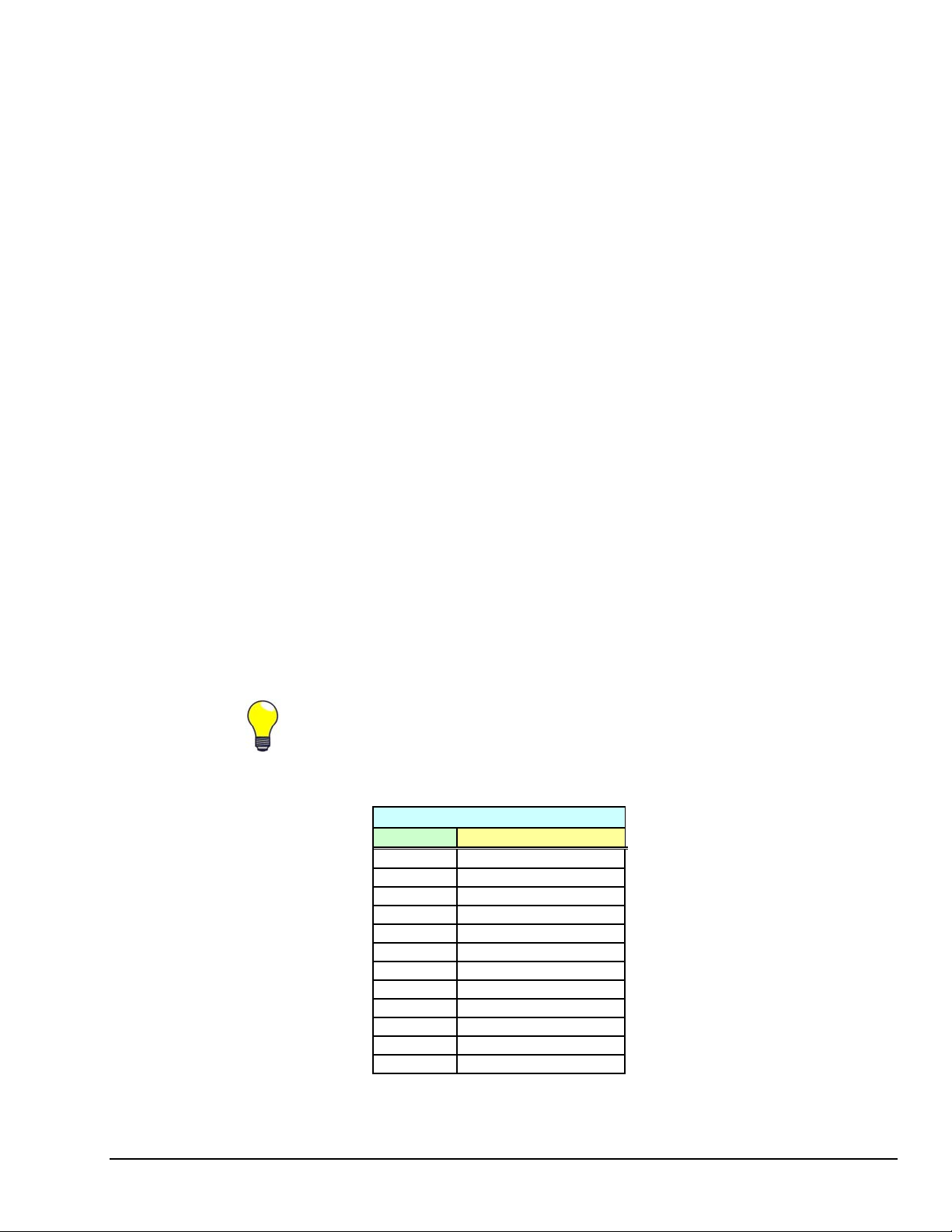
Typical input gain settings are shown in the following table.
Input Gains and Typical Readings
Input Gain Reading
x100 0.5 volts
x200 1.0 volts
x300 1.5 volts
x400 2.0 volts
x500 2.5 volts
x600 3.0 volts
x700 3.5 volts
x750 3.75 volts
x800 4.0 volts
x900 4.5 volts
x1000 5.0 volts
x1200 6 volts *
* requires primary acquisition device to be in unipolar mode.
DBK Option Cards and Module 877095 DBK 43A, pg. 17
Page 38
11. Adjust the Scaling Gain.
(a) DaqView users: select “Scaling Gain” for the Channel Type.
LogView users: select “SetScalingGain” for the Mode.
(b) With the Reading column enabled, adjust the SCALE trimpot (SCA) for a voltage reading
x G
equal to .005 x G
where “GI” is the desired input amplifier gain and “GS” is the
I
S,
desired scaling amplifier gain. Note that each of the eight channels has a channel-specific,
trimpot for Scaling Gain.
(c) Stop the Readings.
Scaling Gains Typical with an Input Gain of x200
Scaling Gain Reading
x2 2.0 volts
x4 4.0 volts
x6 6.0 volts*
x8 8.0 volts*
x10 10.0 volts*
* requires primary acquisition device to be in unipolar mode.
12. Adjust the Offset while the bridge circuit is being read.
(a) Select “Bridge.”
(b) With the Reading column enabled, and with the qu iescen t (normal or inactive) load or strain
applied, adjust the OFFSET trimpot for a reading of 0.00 volts. This adds offset to the
circuit to compensate for the quiescent load and allows maximum resolution for the
measurement.
(c) After adjusting the Offset to 0.00, stop the Readings.
The Offset adjustment is unipolar 0 to 5 V on the input amplifier output. If the Offset can
not be adjusted to 0.00 V at the end of the setup procedure, swap the V
+ (4) and Vin- (3)
in
wire connections, or reduce the Input Gain and increase the Scaling Gain.
13. If required for your application, enable the low-pass filters. The filters are set via jumpers JPn04
where n is the channel number (1 through 8); for example, JP104 sets the filter for channel 1, and
JP804 sets the filter for channel 8.
14. If required for your application, set AC Coupling. Coupling is set via jumpers JPn03 where n is the
channel number (1 through 8). To set AC Coupling, remove the JPn03 jumpers.
15. Calculate the LogBook or Daq device voltage/transducer units. Do this using the transducer
specifications and the total gain of the DBK43A channel. Apply the units to your readings.
16. Verify the software settings by using a known load or strain and comparing the value to that
observed in DaqView’s Reading column.
Note:
Gain adjustments can be made by activating a shunt-cal resistor that is calculated to be at
maximum load.
To enable shunt-cal resistors:
(a) Select “Shunt Cal” as the Channel Type.
(b) Place the DBK43A’s CAL/NORM switch in the CAL position.
(c) LogView users: set th e software CAL/NORM switch, in Hardware
Configuration, to “CAL.”
Settings can be verified via shunt-calibration.
After the final offset is made, the gain readings will be incorrect unless the circuit
offset is removed.
DBK43A, pg. 18 877095 DBK Option Cards and Modules
Page 39
GageCal, Calibration Program for DBK16 and DBK43A in Daq Applications
GageCal is intended for DBK16, DBK43, and DBK43A load cell applications in
conjunction with Daq devices.
GageCal is not used for LogBook applications.
GageCal is a calibration aid for use with DBK16, DBK43, and DBK43A devices that are being used in
Daq device data acquisition systems. The program, which is independent of DaqView, provides an onscreen walk-through for setting jumpers, switches and adjusting trimpots.
With GageCal you can:
• Use a graphic representation of a strain-gage board as a guide to configure switches, jumpers,
and other hardware settings.
• Enter all the parameters pertaining to your strain gage application.
• Follow step by step prompting to adjust trimpots for scale gain, input gain, and offset to ensure
the channel provides the desired input range.
GageCal is installed from the Master Setup screen of the data-acquisition CD-ROM as part of the
DaqBook/DaqBoard Support option. After your DaqBook/DaqBoard support has been installed you can
access and use GageCal as follows.
1. Access GageCal from a desktop shortcut, or by navigating from the desktop as follows:
Start ⇒ Programs ⇒ Omega DaqXSoftware ⇒ GageCal
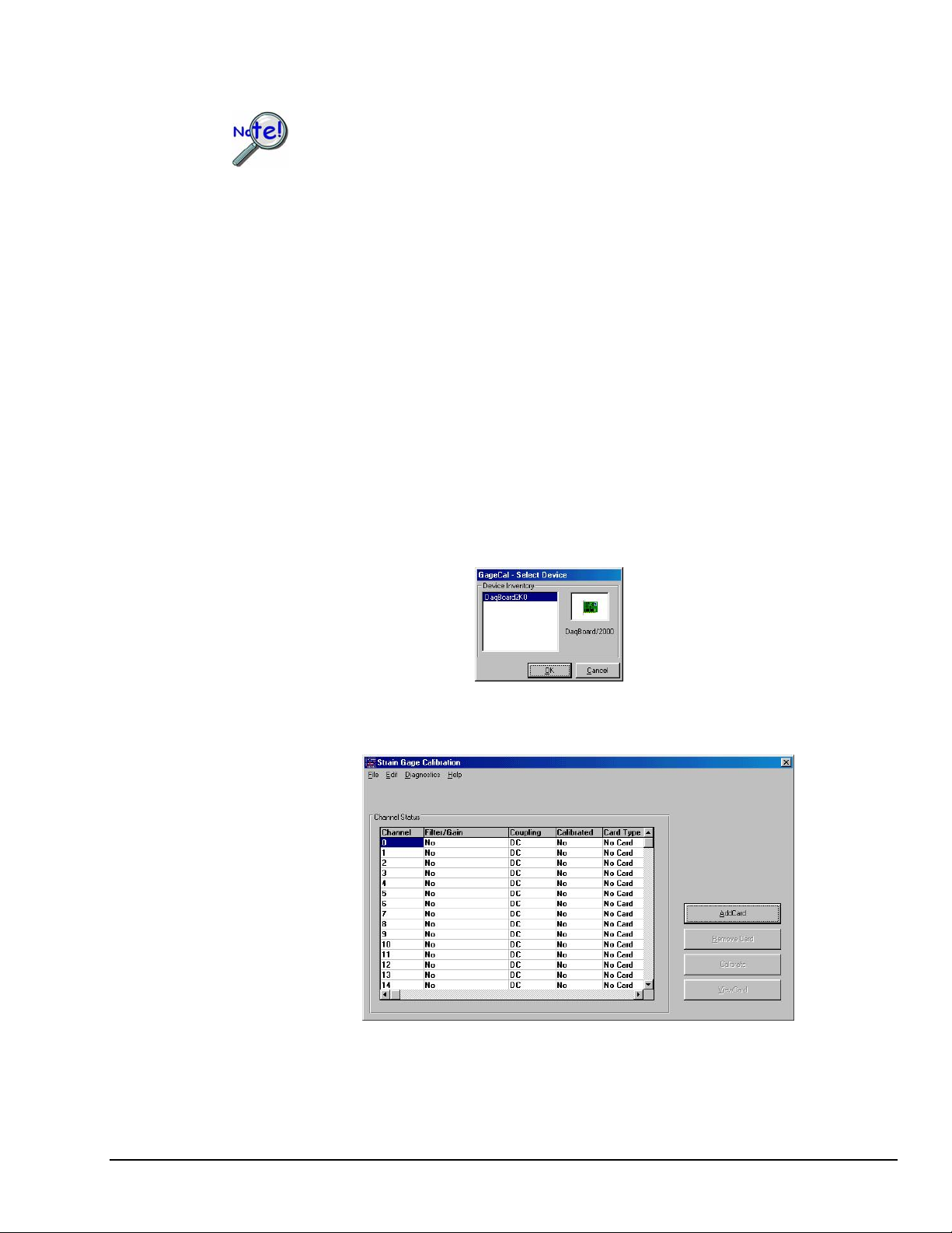
A Select Device window will appear, similar to that shown in the following figure.
GageCal – Select Device
2. From the Select Device window, highlight the applicable DaqBook or DaqBoard, thin click
the <OK> button. The Strain Gage Calibration window will appear.
GageCal’s Strain Gage Calibration Window
3. Click the <AddCard> button. Then select one of the following, as applicable:
DBK16, DBK43, or DBK43A. See following figure.
DBK Option Cards and Module 877095 DBK 43A, pg. 19
Page 40
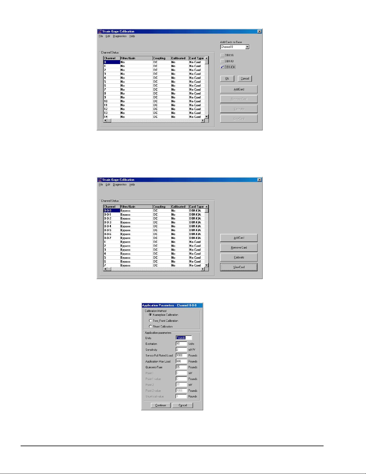
Selecting DBK43A
4. Click the <OK> button. The Strain Gage Calibration window will provide 3 digit channel
numbers in the form of “n
card, and n
is the channel number. See following figure.
3
;” where n1 is the card number, n2- is the bank number on the
1-n2-n3
Strain Gage Calibration Window after Adding a Card
5. Click the <Calibrate> button. An Applications Parameter box appears. See following figure.
Application Parameters for Channel 0-0-0
DBK43A, pg. 20 877095 DBK Option Cards and Modules
Page 41
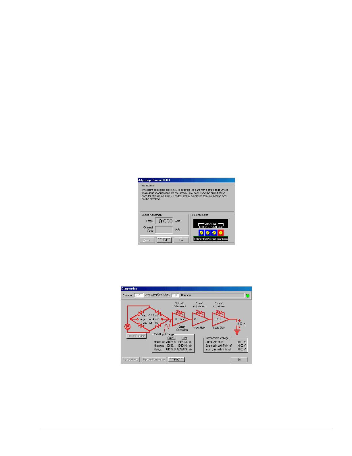
6. Select the type of calibration to be performed, i.e., Nameplate, Two-Point, or Shunt. Then
edit the Application Parameters, if applicable. A brief description of the three calibration
methods follows. When done, click the <Continue> button.
• Nameplate calibration provides a way to enter parameters for your strain gage
and its application. The final step of the procedure includes attaching the strain
gage (load cell).
• Two-Point calibration provides a way to calibrate a DBK16, DBK43, or
DBK43A that is using a strain gage with unknown specifications. In this
method, the user enters two points of transducer output [milli-volts] vs.
engineering units, e.g., pounds. Gage call provides set up instructions based on
the parameters entered. The final step of the procedure includes attaching the
strain gage (load cell).
• Shunt calibration provides a means calibrating channels with use of user-
supplied shunts to simulate a physical load. With this method, 1 or 2 shunt
resistors (Rn00D and Rn00H) are added for each of the 8 channels to be
calibrated. You must set J3 to the position closest to TP9 for the shunt
calibration to work correctly. Shunt calibration is performed with the load-cell
attached.
7. Follow GageCal’s screen prompts to complete the calibration.
Example Screen Shot from GageCal
Note: You can use GageCal’s “Diagnostics” feature to view a graphic representation
of the strain gage and the card’s gain stages.
GageCal Diagnostics
8. After completion, go to DaqView and convert ±5 V to engineering units using mx+b.
DBK Option Cards and Module 877095 DBK 43A, pg. 21
Page 42

DBK43A, pg. 22 877095 DBK Option Cards and Modules
Page 43
Calibrating DBK16 and DBK43A for LogBook Applications
Overview …… 23
Calibration Methods …… 24
Procedures Common to All Calibration
Steps (Required) ……25
Nameplate Calibration and
Manual Calibration ……28
Overview
Calibrating a strain gage channel includes:
One-time adjusting of the bridge excitation.
One-time tuning of the electronic gains and offset via trimpots to maximize performance and
dynamic range.
Applying a transfer function to the voltage output to convert it to engineering units, e.g., pounds,
kilograms.
Executing a software scale and offset adjustment periodically to maintain accuracy.
Channel Calibration Procedure ……31
2-Point Calibration ……34
Shunt Calibration ……36
Creating a Units Conversion Transfer Function ……38
Periodic Calibration Without Trimpots ……38
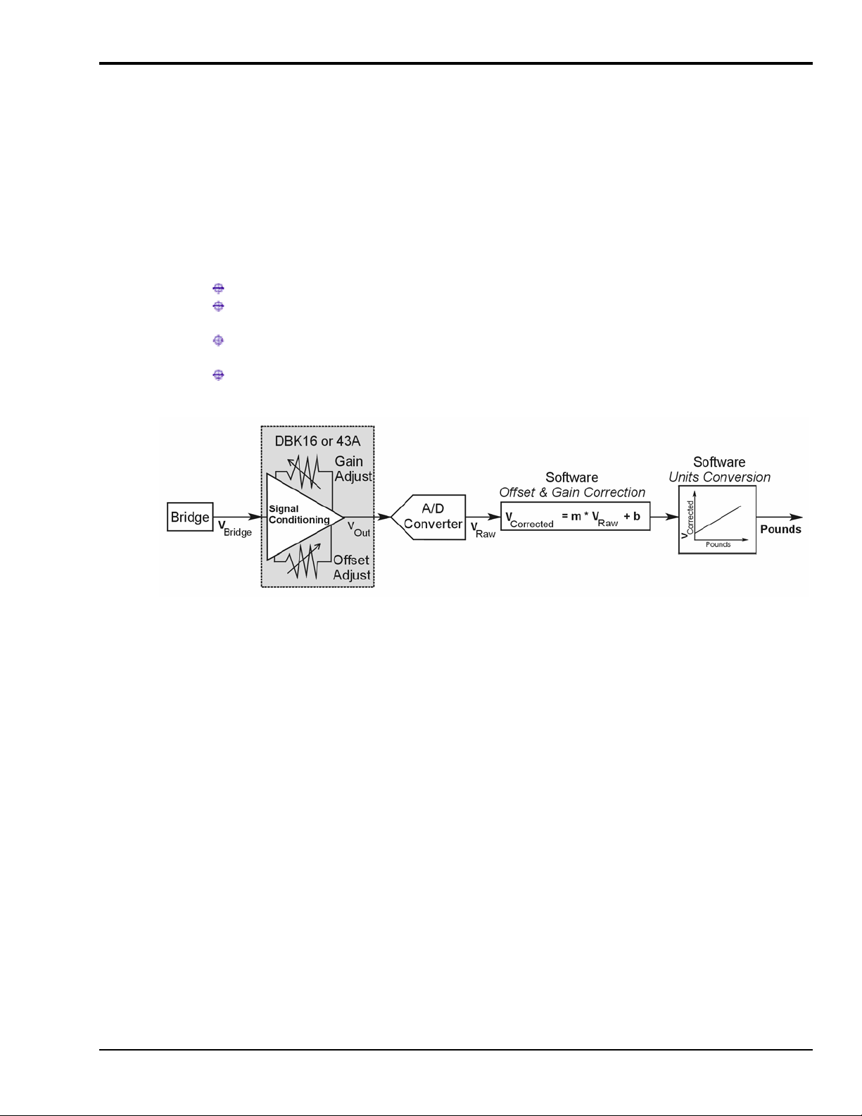
Example of a Unit Conversion from Voltage to Pounds
The trimpots provide course tuning so large quiescent offsets can be nulled and the bridge signal can be
amplified to match the A/D input range. Once these adjustments are made, the operator can periodically
fine-tune the calibration via software using LogView’s 2-Point calibration feature. LogView’s scale and
offset features provide a simple means to apply a transfer function that converts the voltage to user units,
for example, pounds, as in the above block diagram.
Bridge circuit transducers are used for many different applications, and the strain gage signal conditioning
modules are flexible enough to support most of them. Each channel circuit has an excitation regulator, a
high gain (x100 to x1250) input amplifier with offset adjustment, a low-pass filter, a scaling (x1 to x10)
amplifier, and a calibration multiplexer.
By using software-controlled multiplexers, on-board reference voltages can be read b y th e data acquisition
system so that precise gains and offsets can be set. LogView provides a means of easily controlling the
calibration multiplexers so that the reference voltages can be displayed while the trimpots are being
adjusted.
DBK Option Cards and Module 877095 DBK 43A, pg. 23
Page 44
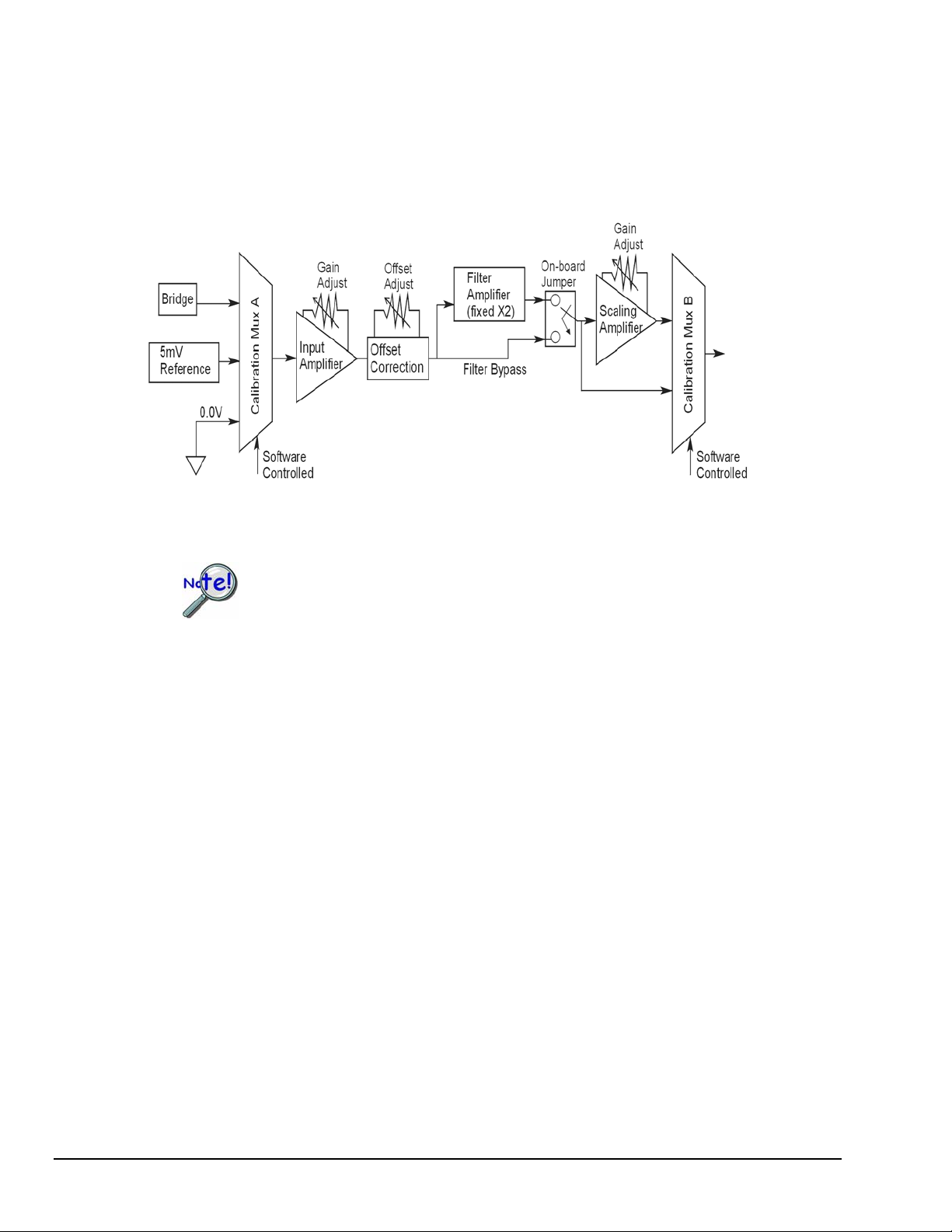
There are four trimpots to set up each channel circuit. The trimpots are labeled to represent the following
adjustments:
• EXC - for adjusting the excitation voltage to the transducer
• GAIN - for setting the gain of the input amplifier
• OFFSET - for adjusting the circuit offset for quiescent loads or bridge imbalance
• SCALE - for setting the gain of the scaling amplifier
Signal-FlowRelationship of Software Controlled Multiplexers and On-Board Reference Voltages
Calibration Methods
Several different calibration techniques are supported by strain gage signal conditioning modules.
Calibration methods include; Nameplate, 2-Point, Shunt, and Manual. From the following discussion,
select the calibration method that is best for your application.
Nameplate – Used to setup the channel using the transducer’s published specs.
Nameplate calibration is typically used with packaged load cells with millivolt-per-volt (mV/V) transfer
functions. Using the mV/V spec of the load cell or a strain gage’s Gage Factor (GF), the necessary system
gain can be calculated and applied to a channel.
2-Point – Used to setup the channel using 2 known loads, one of which might be “no load.”
The 2-Point calibration method requires the operator to apply two known loads to the load cell or strain
gage, one at a time, while the data acquisition system takes measurements. Typically, the first point is with
no load applied and the second point is close to the maximum load capacity of the gage. While measuring
the first point the offset is nulled, and while measuring the second point the gain is adjusted to span the
majority of the input range of the A/D. No gain calculations are required to perform this calibration
method.
This calibration procedure can only be executed while LogBook is attached to a PC that
is running LogView.
To adjust trimpots, use one of the following calibration methods, as appropriate.
DBK43A, pg. 24 877095 DBK Option Cards and Modules
Page 45
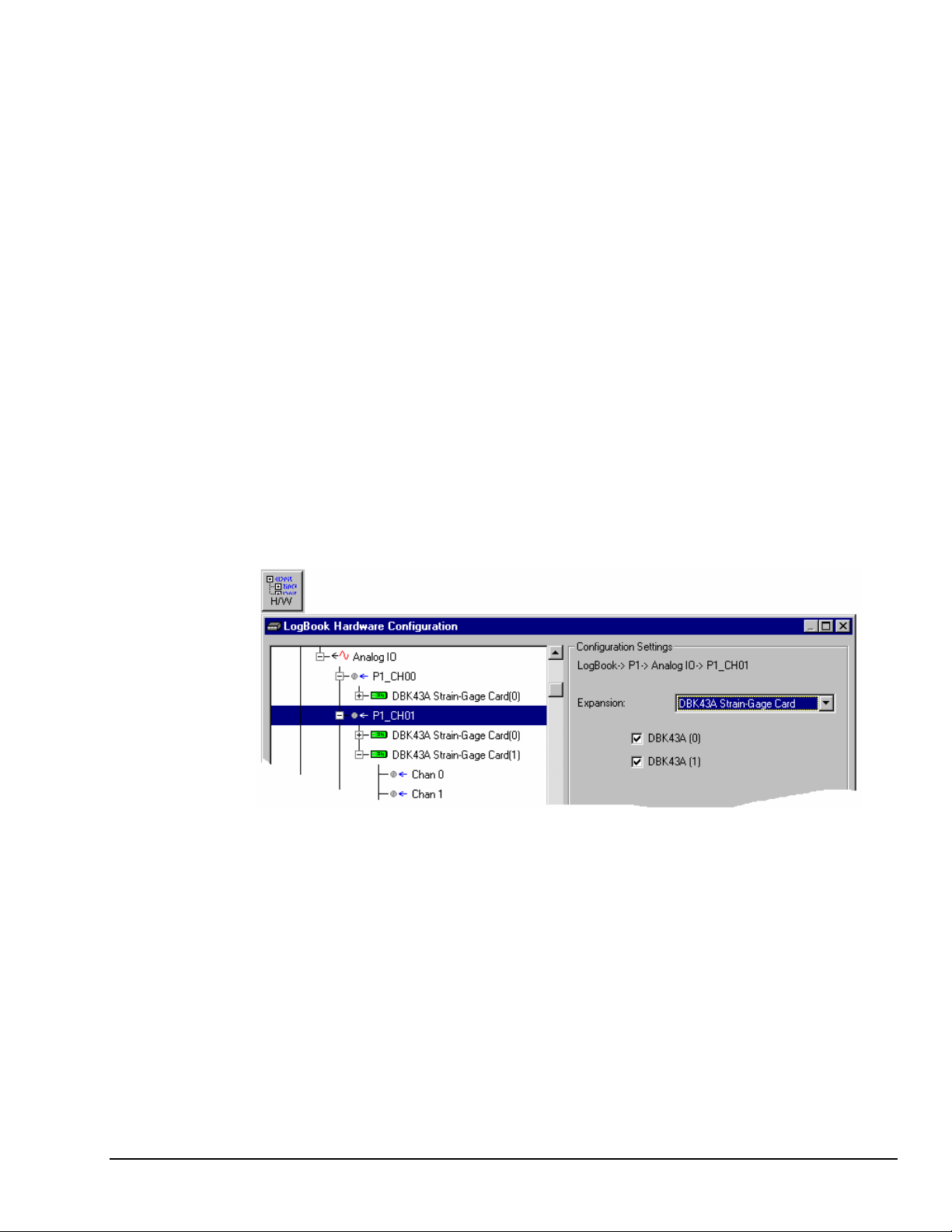
Shunt – Used to setup the channel using a shunt resistor applied to the bridge to simulate a load.
Shunt calibration is identical to 2-Point calibration except that the second point is simulated so that
applying a load near the gage’s maximum load is unnecessary. To simulate a bridge imbalance, a shunt
resistor is placed across one leg of the bridge. Once the shunt resistor value has been calculated, it is
applied to the bridge to provide the desired simulated load. No gain calculations are required to perform
this calibration method.
Manual – Used to assign specific gains and offsets.
If a particular gain and offset are already known, these values can be used to setup a strain gage channel.
Procedures Common to All Calibration Steps (Required)
Set the Selected Channel(s) to DC Coupling
Since the applied calibration-signals are DC, set DC coupling for all the channels that are being adjusted.
If your application requires AC coupling, don’t forget to remove the jumpers when the adjustment
procedure has been completed.
Determine Channel Parameters
Before adjusting the trimpots, the excitation needs to be determined. Typically, the supplier of the gage of
load cell will recommend a suitable value, but make sure that the maximum output current of the excitation
regulator is not exceeded.
Initialize LogView
Launch LogView and use the LogBook Hardware Configuration window (hardware tree) to configure all
of the DBK options that are to be used in the system. If needed, refer to the LogView chapter of the
LogBook User’s Manual (p/n 461-0901).
LogBook Hardware Configuration, Button and Screen
Open the Analog Input Channel Configuration Window. Click the User Scaling Tab and verify that all of
the strain gage channels that are to be adjusted have scale and offset values of 1 and 0, respectively.
DBK Option Cards and Module 877095 DBK 43A, pg. 25
Page 46
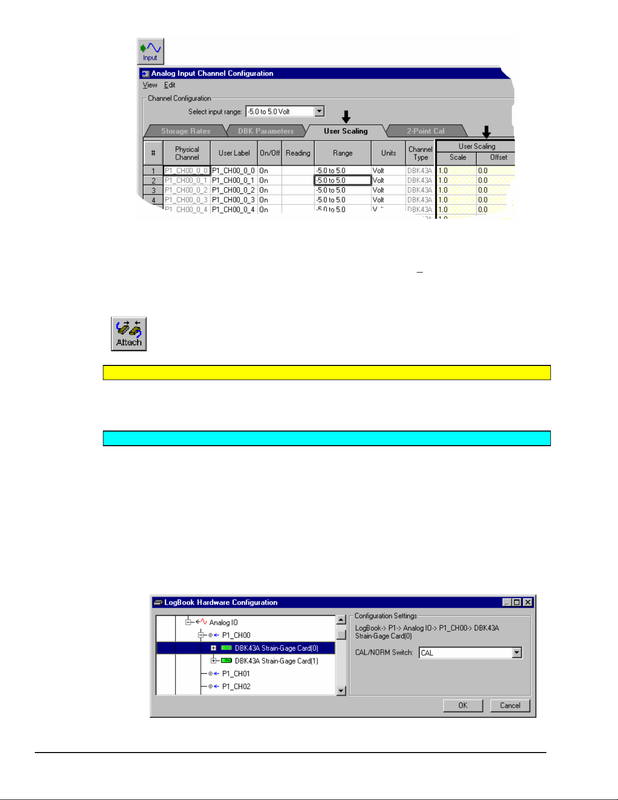
Analog Input Channel Configuration Window, Button and Screen … “User Scaling” Tab Selected
For all of the strain gage channels that are to be adjusted, set their ranges to
+5V.
Click the DBK Parameters tab to expose the strain gage signal conditioning programmable settings.
Click the Attach button to substantiate a connection between the PC and the LogBook.
Adjust the Excitation - DBK16
For DBK16, set the excitation voltage for the transducer by adjusting the trimpot labeled EXC and
measuring the voltage with a voltmeter across the +EXC and -EXC on the bridge or at the terminals of the
signal conditioning module.
Adjust the Excitation - DBK43A
DBK43A is equipped with a switch that allows the excitation voltage to be read by the LogBook and
displayed in LogView. For all DBK43A units to be adjusted, you must:
1. Reposition the DBK43A’s “physical” calibration switch (located next to the Power LED) to
the CAL position.
2. Select CAL in LogView. This is detailed in the following paragraph.
Open the LogBook Hardware Configuration window and select DBK43A (see following
figure). In the Configurations settings box, set the CAL/NORM Switch to CAL. If the
DBK43A is not displayed click the + to the left of the base channel (to which it is attached),
this action expands the hardware tree in the LogBook Hardware Configuration window.
Repeat this process for all DBK43A units that are to be adjusted. Click OK to lock in the
changes.
Setting a DBK43A Cal/Norm Switch to “CAL”
DBK43A, pg. 26 877095 DBK Option Cards and Modules
Page 47
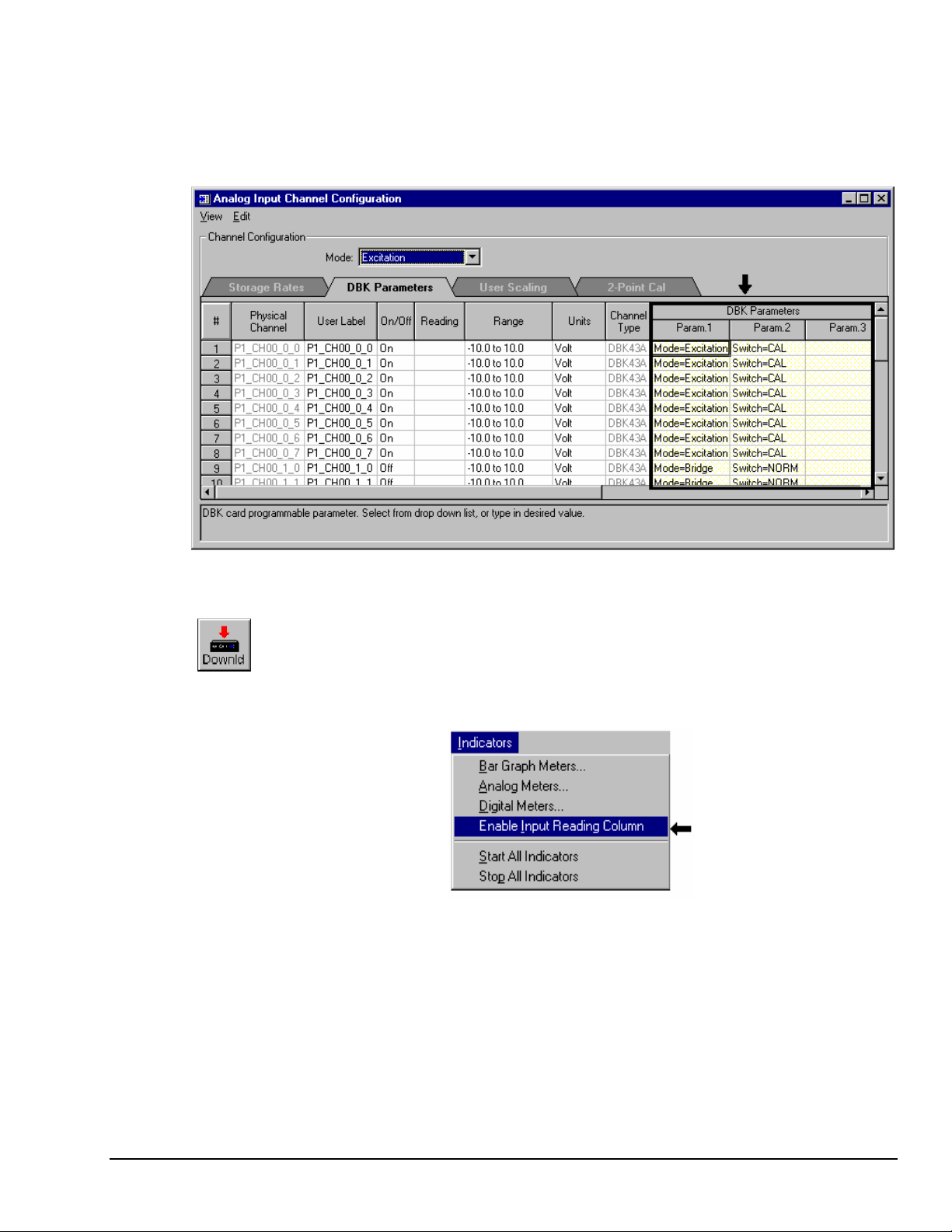
3. In the Param1 column (see next figure for location), select all of the DBK43A channels that
are to be adjusted.
4. Set Mode equal to Excitation from the drop down list (located above the DBK Parameters
tab).
5. Turn off all the channels in the system except for those DBK43A channels that are to be
adjusted.
Selecting “Mode = Excitation” for DBK Parameter 1
6. Click the Download button to send the current configuration to the LogBook.
7. Select Indictors \ Enable Input Reading Column from the menu bar to display the
excitation values for each channel.
Selecting “Enable Input Reading Column”
(from the Indicators Pull-Down Menu)
8. Set the excitation voltage for each transducer by adjusting the trimpot labeled EXC for the
associated channel while reading their values in LogView.
9. Select Indictors \ Disable Input Reading Column from the menu bar.
DBK Option Cards and Module 877095 DBK 43A, pg. 27
Page 48

Selecting “Disable Input Reading Column”(from the Indicators Pull-Down Menu)
10. Return the physical calibration switches (of the applicable DBK43As) to the NORM position.
11. In LogView, open the LogBook Hardware Configuration Window (hardware tree) and select
NORM for each DBK43A.
This completes the section entitled: “Procedures Common to All Calibration Steps (Required)”
Nameplate Calibration and Manual Calibration
To properly calibrate a strain gage channel using the Nameplate method, the required gain must first be
calculated. If the desired gain and offset are already know [as in the Manual calibration method] skip to
the section, Determining the Gain of Each Amplification Stage.
The following examples outline the necessary steps for determining the required gain for
Nameplate calibration. Both strain gage and load cell examples are provided.
Calculating the Required Gain
Determining a Strain Gage’s Maximum Output Voltage
Most strain gages come with Gage Factors (GF) used to calculate the approximate output of the bridge
circuit with a typical strain value. The formula is:
V
BR
= (V
* G * S * B) / 4 [See following important notice.]
EXC
Where: VBR = Bridge output voltage
V
= Excitation Voltage
EXC
G = Gage Factor
S = Strain in user units (in uStrain)
B = Configuration factor (1 for ¼ bridge, 2 for ½ bridge, 4 for full bridge)
The equation, V
BR
= (V
* G * S * B) / 4 produces a linear estimate. If you are
EXC
using a non-linear strain gage you should refer to strain gage theory for additional
information as needed.
For a 120 ohm strain gage with a gage factor of 2.1 and excitation voltage of 5 V, applying
4000 microstrain would produce an bridge output of 10.5mV for a ¼ bridge configuration.
V
= (5 * 2.1 * 4000x10-6) / 4 = 10.5 mV
BR
DBK43A, pg. 28 877095 DBK Option Cards and Modules
Page 49

Determining a Load Cell’s Maximum Output Voltage
Load cells come with a mV/V specification—for each volt of excitation at maximum load, the load cell
will output a specific millivolt level.
V
= R * V
LC
EXC
Where: V
= Load cell output voltage
LC
R = Load cell spec (mv/V)
V
= Excitation voltage
EXC
Consider a 3000 pound load cell rated at 2.05 mV/V using 10 V of excitation (assume a 350Ω load cell).
When 3000 pounds is applied, the voltage out of the load cell is 20.5mV.
V
= (10 * 2.05×10-3) = 20.5 mV
LC
If 1000 pounds were applied, we would see 6.833 mV. This is arrived at as follows:
-3
(1000/3000) * 10 * 2.05×10
= 6.833 mV
Using the Calculated Maximum Voltage to Determine the Necessary Gain
To maximize the resolution and dynamic performance of the system, the sensor’s output should be
amplified to correspond to the data acquisition system’s input range.
Using the LogBook’s
+5V input range, the required gain is calculated by dividing 5V by the maximum
output voltage of the sensor. Before performing the calculation, it is typically a good idea to pad the
maximum sensor voltage by about 5% so that, once amplified, it won’t bump into the limit of the 5V range.
G = V
/ (VGO + VGO * 5%)
LB
Where: G = Gain
V
V
= LogBook input range
LB
= Maximum gage output
GO
For the strain gage in the previous example with a maximum output of 10.5mV, the required gain is:
G = 5.0V / (0.0105V + 0.0105V * 0.05) = 453.5
For the above load cell with a maximum output of 20.5mV, the required gain is:
G = 5.0V / (0.0205V + 0.0205V * 0.05) = 232.3
DBK Option Cards and Module 877095 DBK 43A, pg. 29
Page 50
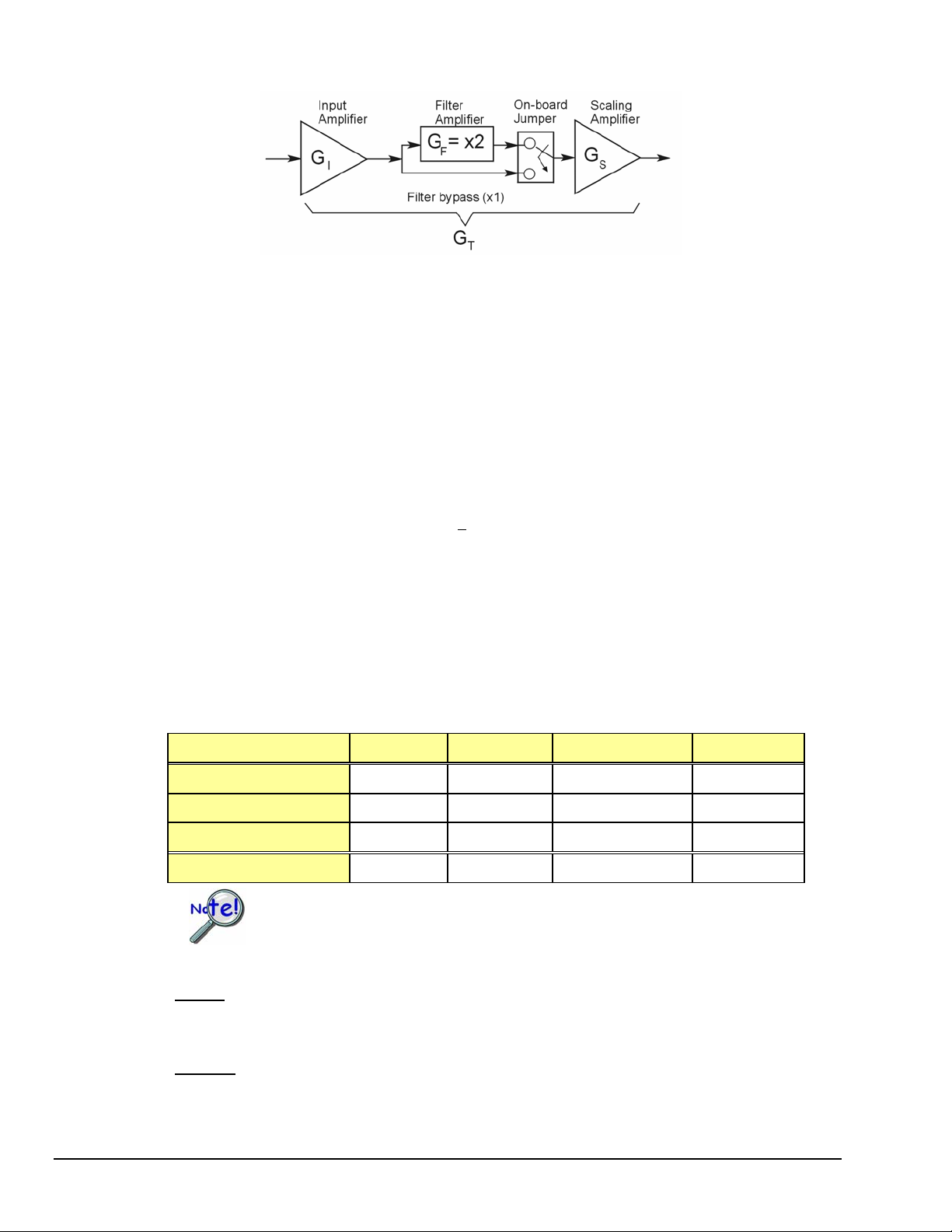
Determining the Gain of Each Amplification Stage
The system’s total gain is:
G
= GI * GF * G
T
S
Where: G
G
G
G
= Total gain
T
= Input amplifier gain
I
= Filter gain
F
= Scaling amplifier gain
S
Note: Maximum gain calibration is x1000 for
+5V range.
The majority of the gain should be assigned to the Input Amplifier, with the Scaling Amplifier used for
fine-tuning. If the filter is enabled, a gain of x2 is automatically introduced.
The input amplifier has a gain range of ×100 to ×1250; the filter gain ×1 or ×2; and the scaling amplifier
has a range of ×1 to ×10. For the strain gage example, if we round off our gain to ×420, any of these
possible settings will work.
Input Gain
Option A Option B Option C Option D
×420 ×100 ×240 ×300
Filter Gain (enabled)
Scaling Gain
Total Gain
No Yes (×2) Yes (×2) *
×1 ×2.1 ×1.75 ×1.4
×420 ×420 ×420 ×420
See Note No
For Option C, the LPF gain is typically x2.
For gains of x1 (if the filter is enabled), the following apply:
DBK16 - For a gain of x1 (if the filter is enabled),10KΩ resistors R44 and R46 must have been
previously removed (for the low and high channels, respectively).
DBK43A - For a gain of x1 (if the channel filters are enabled), removal of the following 10 KΩ
resistors applies: Ch0 – R144, Ch1 – R244, Ch3 – R444, Ch4 – R544,
Ch5 – R644, Ch6 – R744, Ch7 – R844.
DBK43A, pg. 30 877095 DBK Option Cards and Modules
Page 51
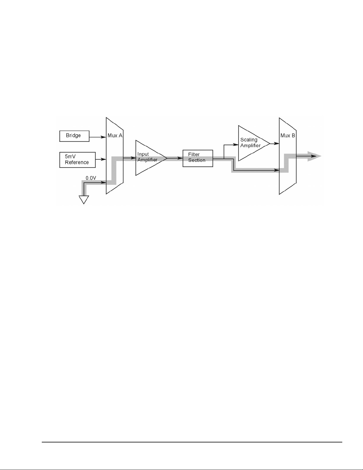
Channel Calibration Procedure
Adjust the Offset
The following steps are used to adjust the offset.
1. In the Param1 column (see page 27 for location), select all of the DBK43A channels that are
to be adjusted.
2. Select Mode = SetOffset from the drop down list above the grid. This selection commands
the calibration multiplexer to route the 0.0V reference through the entire analog path (see
following figure).
“Mode = Offset” 0.0 Volt Reference is Routed
3. Turn off all the channels in the system except for those DBK43A channels that are to be
adjusted.
4. Click the Download button. This sends the current configuration to the LogBook.
5. Select Indictors \ Enable Input Reading Column from the menu bar. This displays the offset
values for the enabled channels.
6. Set the offset voltage to 0.0V for each transducer by adjusting the trimpot labeled OFFSET
for the associated channel.
7. Select Indictors \ Disable Input Reading Column from the menu bar.
Adjust the Input Amplifier Gain
Perform the following steps to adjust the Input Amplifier Gain.
1. In the Param1 column (see page 27 for location), select all of the DBK43A channels that are
to be adjusted.
2. Select Mode = SetInputGain from the drop down list above the grid. This selection
commands the calibration multiplexer to route a 5mV reference through the Input Amplifier
and bypass the Scaling amplifier (see following figure).
Note: If the filter is enabled (not bypassed) accommodate an additional x2 gain stage.
DBK Option Cards and Module 877095 DBK 43A, pg. 31
Page 52
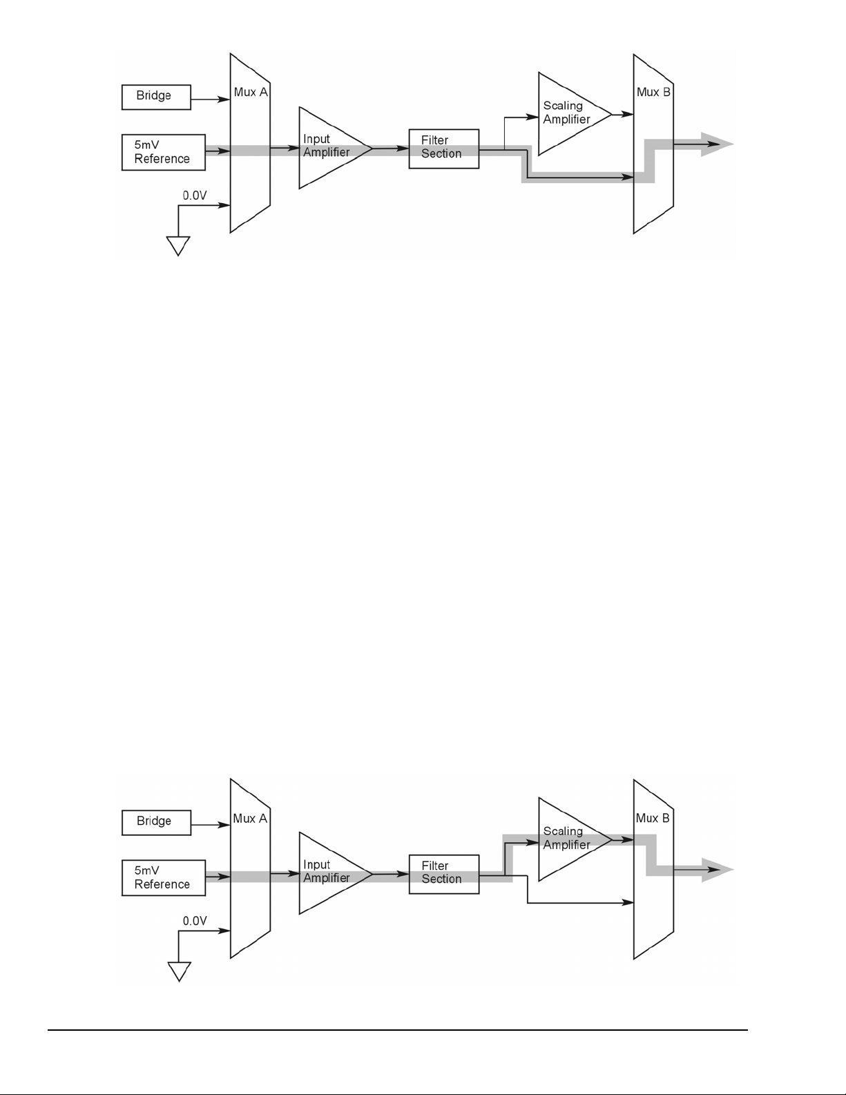
“Mode = SetInputGain,” 5 milli-Volt Reference Route
3. Turn off all the channels in the system except for those DBK43A channels that are to be
adjusted.
4. Click the Download button to send the current configuration to the LogBook.
5. Select Indictors \ Enable Input Reading Column from the menu bar to display the values for
each channel.
6. For the associated channel, set the voltage to [G
adjusting the trimpot labeled GAIN. Use the Input Amplifier Gain (G
Note: If the filter is enabled, the filter gain (G
Example 1: If G
trimpot would be adjusted to obtain 1.25V.
Example 2: If G
trimpot would be adjusted to obtain 2.50V.
7. Select Indictors \ Disable Input Reading Column from the menu bar.
Adjust the Scaling Amplifier Gain
Adjust the Scaling Amplifier Gain as follows:
1. In the Param1 column (see page 27 for location), select all of the DBK43A channels that are
to be adjusted.
2. Select Mode = SetScalingGain from the drop down list above the grid. This selection
commands the calibration multiplexer to route a 5mV reference through all of the
amplification stages as shown below.
* GF * 0.005] for each transducer by
I
) calculated earlier.
I
) is 2; otherwise GF = 1.
F
= 250 and the filter is disabled; the GAIN
I
= 250 and the filter is enable; the GAIN
I
“Mode = ScalingGain,” 5 milli-Volt Reference Route
DBK43A, pg. 32 877095 DBK Option Cards and Modules
Page 53
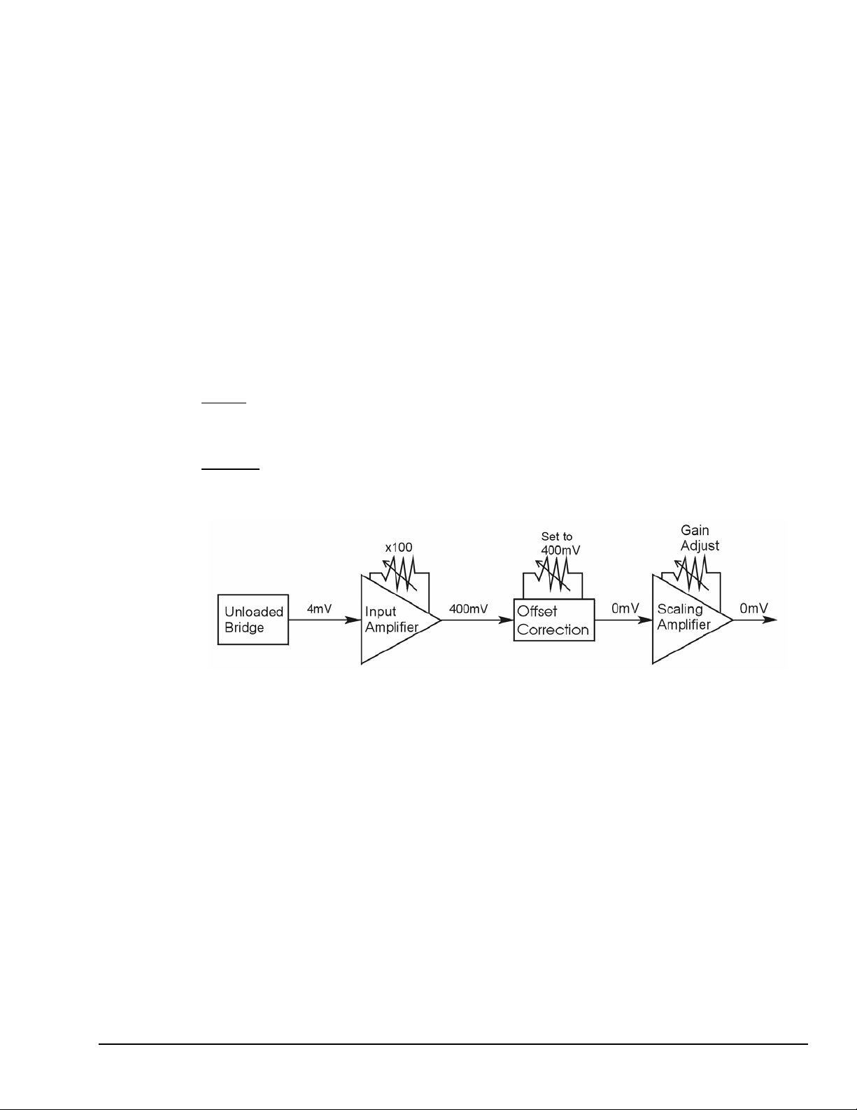
3. Turn off all the channels in the system except for those DBK43A channels that are to be
adjusted.
4. Click the Download button to send the current configuration to the LogBook.
5. Select Indictors \ Enable Input Reading Column from the menu bar to display the values for
each channel.
6. For the associated channel, set the voltage to [G
the trimpot labeled SCALE. Use the total system gain (G
Example: If G
= 435.5, the SCALE trimpot would be adjusted to obtain 2.17 V.
T
* 0.005] for each transducer by adjusting
T
) calculated earlier.
T
7. Select Indictors \ Disable Input Reading Column from the menu bar.
Trimming Bridge Quiescent Load
Most bridges have some level of offset, even if no quiescent load is present. In quarter and half bridge
situations, use of 1% bridge completion resistors can cause up to 1mV/V of offset. If the bridge has 4mV
of offset and the Input Amplifier is set to x100, the Offset potentiometer would need to nullify 400mV.
DBK16 – For DBK16s, the Offset Potentiometer can adjust out 0 to +5V of offset amplified by the
Input Amplifier.
DBK43A – For DBK43As, the Offset Potentiometer can adjust out -1.25 to +5V of offset amplified by the
Input Amplifier.
Trimming Bridge Quiescent Load
If a significant amount of quiescent offset is present and the Input Amplifier gain is set too high, the
Offset Potentiometer will not have enough range to adequately nullify the offset. In this case, the gain of
the Input Amplifier must be reduced while the gain of the Scaling Amplifier is increased proportionately.
Use the following steps to trim bridge quiescent load (unload the bridge).
1. In the Param1 column (see page 27 for location), select all of the DBK43A channels that are
to be adjusted.
2. Select Mode = Bridge from the drop down list above the grid. This selection commands the
calibration multiplexer to route the transducer output through the analog path as shown
below.
DBK Option Cards and Module 877095 DBK 43A, pg. 33
Page 54
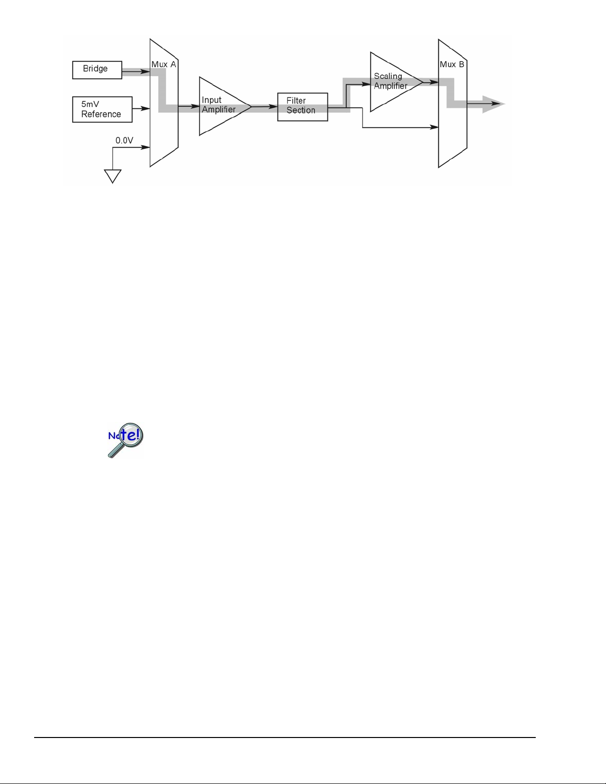
2-Point Calibration
“Mode = Bridge,” Reference Route
3. Turn off all the channels in the system except for those DBK43A channels that are to be
adjusted.
4. Click the Download button to send the current configuration to the LogBook.
5. Select Indictors \ Enable Input Reading Column from the menu bar to display the offset
values for each channel.
6. For the associated channel, set the offset voltage to 0.0V for each transducer by adjusting the
trimpot labeled OFFSET.
Note: If you are unable to nullify the quiescent offset of the bridge, your Input Amplifier
gain may be too high. Information regarding gain redistribution can be found in the
section entitled, Determining the Gain of Each Amplification Stage.
7. Select Indictors \ Disable Input Reading Column from the menu bar.
This 2-point calibration method makes use of trimpot adjustments. It should not be
confused with the LogView software 2-Point Calibration (discussed in the LogView
chapter in the LogBook User’s Manual).
In the 2-Point calibration method, the user places two known loads on the gage, one at a time, then adjust
the trimpots until the expected value is reached. Typically, the first of loads is “no load.” In the case of a
weight scale, the scale would first be unloaded to adjust the offset, then a known load (near maximum
expected) would be applied to adjust the gain.
Shunt calibration (discussed immediately after this 2-Point Calibration section) is the same as the 2-Point
method, except the second load is applied in a simulated fashion by shunting 1 leg of the bridge with a
shunt resistor. Shunt calibration is preferred in cases where applying a real load (near the maximum
expected) is not practical.
Initialize the System
1. Download a single setup and continuously display data in LogView. The continuous display
can remain throughout the procedure since the calibration multiplexers do not need reset
between steps.
2. In the Param1 column (see page 27 for location), select all of the DBK43A channels that are
to be adjusted.
3. Select Mode = Bridge from the drop down list above the grid. This selection commands the
calibration multiplexer to route the transducer voltage through the analog path.
DBK43A, pg. 34 877095 DBK Option Cards and Modules
Page 55

4. Turn off all the channels in the system, except for those DBK43A channels that are to be
adjusted.
5. Click the Download button to send the current configuration to the LogBook.
6. Select Indictors \ Enable Input Reading Column from the menu bar to display the offset
values for each channel.
Adjust the Offset
For the associated channel, apply the first calibrated load to each gage (typically no-load) and set the
voltage to 0.0V for each transducer. This is accomplished by adjusting the trimpot labeled OFFSET. If the
first point is actually a calibrated load, you will need to move the load to each gage, one at a time, to adjust
its associated offset.
Adjust the Input and Scale Amplifier Gain
Complete the following steps to adjust the channel gain.
1. Apply the second load to each gage channel. The value of this load should approximate that
of the maximum expected load. For the best results, a gain should be selected so that the
bridge’s maximum output equals 90% of the A/D’s input range.
2. Calculate the desired voltage for the second point using the following equation:
V
Where: V
L
L
V
= (LA/LM) * VI * 90%
D
= Desired voltage for 2nd point of calibration
D
= Applied load used in calibrating the 2nd point
A
= Maximum load expected during usage
M
= Input voltage range
I
Example: The load standard that will be applied to the gage as the 2
calibration is 100lbs. The maximum expected load during usage is 150lbs.
The programmable input range of the data acquisition system is set for
The desired output voltage of the strain gage signal conditioning electronics is:
= (100/150) * 5 * 0.90 = 3V
V
D
In this example, we should adjust the GAIN and SCALE trimpots until a value of 3V is
measured.
If 150 lbs is applied to the gage, a voltage of 4.5V will be measured.
= (150/150) * 5 * 0.90 = 4.5V
V
D
3. Apply the second calibrated load to each gage and set the voltage to V
Do this for each transducer by adjusting the trimpots labeled GAIN and SCALE for the
associated channel. Note that the GAIN trimpot provides most of the amplification (course
adjustment), while the SCALE trimpot allows for fine-tuning.
nd
point in the 2-Point
+5V.
, as derived in step 2.
D
Repeating the Process
Since adjusting the gain for the first time will have an affect on the offset, it is recommended that offset and gain adjustment be performed twice for each channel.
DBK Option Cards and Module 877095 DBK 43A, pg. 35
Page 56

Shunt Calibration
Shunt calibration is virtually identical to the 2-Point method just discussed, except that the second point is
simulated. The simulated load is achieved by shunting one leg of the bridge with a shunt resistor. Shunt
calibration is the preferred calibration method when applying a real load (of a value approximating the
maximum expected load) is not practical. To adjust the channel gain, the shunt must be applied to the
bridge.
Adjust the Offset
Adjust the offset as follows.
Calculate and install the necessary shunt resistor before continuing.
DBK43A has direct support for shunt calibration, accommodating the
resistor in its enclosure and allowing the software to apply it when requested.
DBK16 does not have direct support, so the shunt resistor must be applied
externally and switched in manually.
1. In the Param1 column, select all of the DBK43A channels that are to be adjusted.
2. Select Mode = Bridge from the drop down list above the grid. This selection commands the
calibration multiplexer to route the transducer voltage through the analog path.
3. Turn off all the channels in the system except for those DBK43A channels that are to be
adjusted.
4. Click the Download button to send the current configuration to the LogBook.
5. Select Indictors \ Enable Input Reading Column from the menu bar to display the offset
values for each channel.
6. For the associated channel, apply the first calibrated load to each gage (typically no-load) and
set the voltage to 0.0V for each transducer by adjusting the trimpot labeled OFFSET.
If the first point is an actual calibrated load, you must move the load to each gage, one at a
time, to adjust its associated offset.
Adjust the Input and Scale Amplifier Gain
For the best results, a gain should be selected so that the bridge’s maximum output equals 90% of the
A/D’s input range.
1. Use the following equation to calculate the desired shunt voltage (V
V
= (Ls/LM) * VI * 90%
D
Where: V
L
L
V
Example: The simulated load produced by the shunt 100lbs. The maximum expected load during
= Desired voltage from the after amplification when the shunt is applied
D
= Simulated load produced by shunt
s
= Maximum load expected during usage
M
= Input voltage range
I
usage is 150 lbs. The programmable input range of the data acquisition system is set
+5V. The desired output voltage of the strain gage signal conditioning electronics
for
is:
).
D
V
= (100/150) * 5 * 0.90 = 3V
D
In this example, we would adjust the GAIN and SCALE trimpots until a value of 3V
is measured.
DBK43A, pg. 36 877095 DBK Option Cards and Modules
Page 57
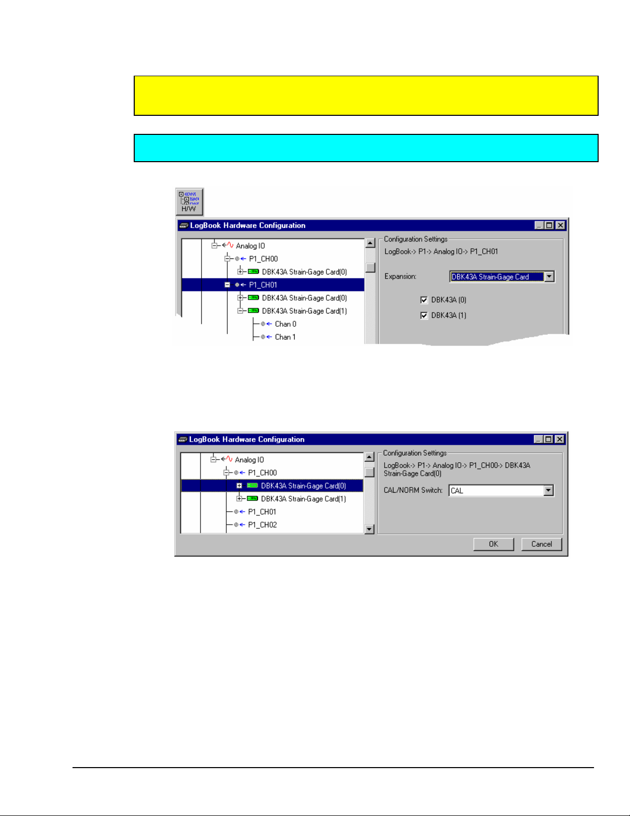
If 150lbs is applied to the gage, a voltage of 4.5V will be measured.
V
= (150/150) * 5 * 0.90 = 4.5V
D
For DBK16, only … Externally apply the shunt resistor and set the voltage to VD, as derived above for each
transducer. This is done by adjusting the trimpots labeled GAIN and SCALE for the associated channel.
The GAIN trimpot is used for course adjustment; and the SCALE trimpot for fine-tuning.
For DBK43A only … DBK43 is equipped with a physical switch that allows the shunt to be applied when
directed by the software. For each DBK43A to be adjusted, move this physical switch from NORM to CAL.
2. In LogView, open the LogBook Hardware Configuration window and select the DBK43A.
LogBook Hardware Configuration, Button and Screen
3. Select the DBK43A from the LogBook Hardware Configuration window’s hardware tree.
4. Set the list box to the right to CAL. If the DBK43A is not displayed click the + to the left of
the base channel to which it is attached to expand the hardware tree.
Setting a DBK43A Cal/Norm Switch to “CAL”
5. Repeat this process for each DBK43A that is to be adjusted.
6. Click OK to lock in the changes.
7. Open the Analog Input Channel Grid. In the Param1 column (see page 27 for location),
select all of the DBK43A channels that are to be adjusted. Select Mode = Shunt from the
drop down list above the grid. Turn off all the channels in the system except for those
DBK43A channels that are to be adjusted.
8. Click the Download button to send the current configuration to the LogBook.
9. Select Indictors \ Enable Input Reading Column from the menu bar to display the excitation
values for each channel.
DBK Option Cards and Module 877095 DBK 43A, pg. 37
Page 58
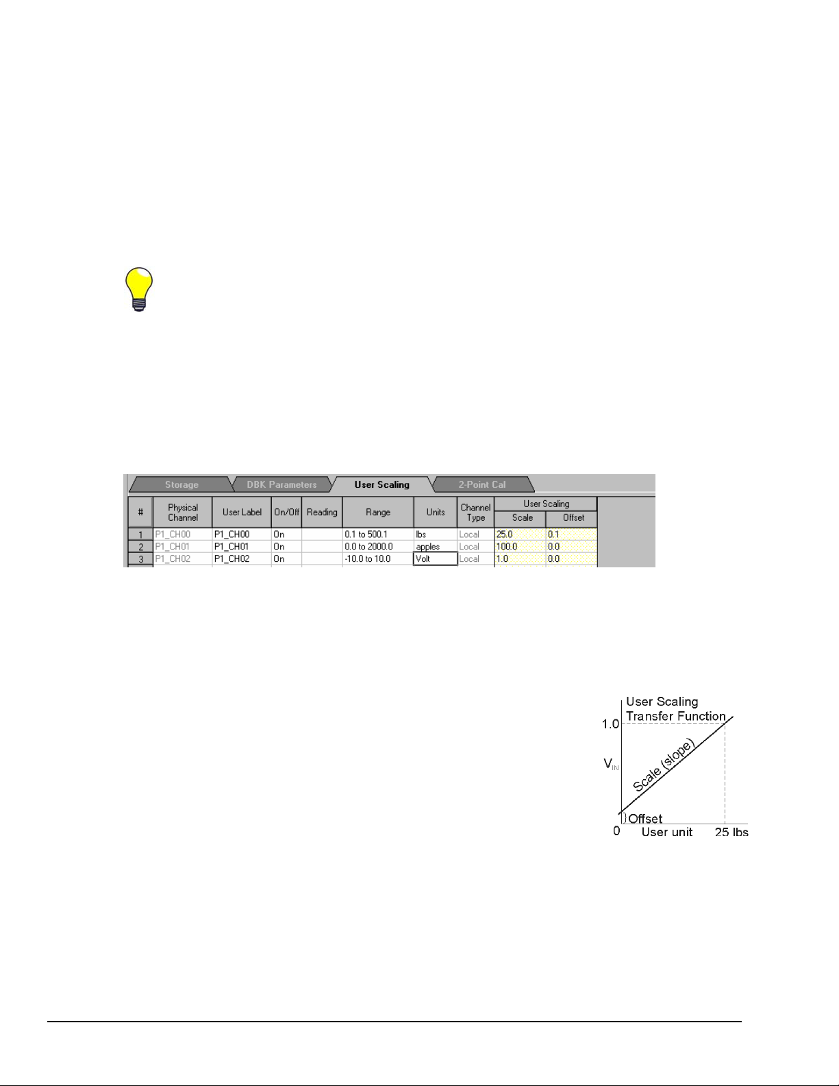
10. Set the voltage to VD, as derived above, for each transducer. This is accomplished by
adjusting the trimpots labeled GAIN and SCALE for the associated channel. The GAIN
trimpot provides for course adjustment. The SCALE trimpot provides for fine tuning.
11. Select Indictors \ Disable Input Reading Column from the menu bar.
12. Return the physical NORM/CAL switches (of the applicable DBK43As) to the NORM
position.
13. In LogView, open the LogBook Hardware Configuration window and return each DBK43A
back to NORM.
Repeating the Process
Since adjusting the gain for the first time will have an affect on the offset, it is recommended that
offset and gain adjustment be performed twice for each channel.
Creating a Units Conversion Transfer Function
To make the data from your gage more useful, it should be recorded in terms of units appropriate to your
application, such as pounds, kilograms, inches, mm, or Hg. A transfer function is needed to convert volts to
these more meaningful units.
For this purpose, LogView provides a means of assigning a mathematical scale and offset to each channel.
Scale and offset information from that chapter has been repeated below for convenience.
In User Scaling, you can create a transfer function. The function allows LogView to display units that could
be more useful to you than volts. For example, you could obtain readings with pounds as the designated Units.
The reading (in pounds) will be based on the raw input value, typically Volts, and the indicated Scale and Offset
adjustment.
To create the transfer function:
1. Type the desired unit name in the Units column.
2. Select an appropriate range (e.g. unipolar).
3. Enter the linear scale relation to Volts (e.g. 25 pounds per Volt).
4. Enter any offset from 0, for example, an empty basket used in an
application reads 0.1 V.
The reading and range columns will automatically change to the adjusted v alues.
Periodic Calibration Without Trimpots
Once the trimpots have been adjusted during initial installation, periodic trimming can be performed
through LogView’s 2-Point software calibration. The LogView procedure does not require the use of
trimmpots and should not be confused with the 2-point method discussed in this section of the manual.
Refer to the LogView chapter in the LogBook User’s Manual for information regarding 2-point calibration
via software.
DBK43A, pg. 38 877095 DBK Option Cards and Modules
Page 59

DBK43A – Specifications
Name/Function: Strain-Gage Module
Connectors: DB37 mates with P1; mini-DIN6 provided for strain-gage or external excitation connections
Number of Channels: 8
Excitation Voltage Adjustment Ranges: 1.50 to 10.50 VDC @ 50 mA
Input Gain Range: ×100-1250; separate instrumentation amplifier for each channel with gain adjustable via
externally accessible 15-turn trimpot
Accommodated Bridge Types:
Full bridge, Kelvin excitation (6-wire)
Full bridge (4-wire)
Half bridge (3-wire)
Quarter bridge (2-wire)
Bridge-Completion Resistors: On-board resistor socket locations (Rn00A, Rn00B, Rn00C, Rn00E, Rn00F,
and Rn00G) for 6 bridge-completion resistors per channel
Input Type: Differential
Input Impedance: 100 MΩ
CMMR: 115 dB
Excitation Current Output: 50 mA max (current limited @ 60 mA)
Excitation Sensing: Local or remote
Excitation Regulation
Line Regulation: 0.025%
Load Regulation: 0.05%
Reference Voltages: 2.5 VDC
Reference Accuracy: 0.05%
Reference Drift: 3 ppm/°C
Gain Calibration Reference: 5 mVDC
Gain Calibration Reference Accuracy: 0.2%
Gain Calibration Reference Drift: 20 ppm/°C
Gain Accuracy: 0.5%
Gain Drift: 50 ppm/°C
Input Offset: 100 µV max
Offset Drift: 4 µV/°C
Output Offset: 20 µV
Offset Drift: 200 µV/°C
Offset Adjustment: 0-100% of range, 0-5 VDC (15-turn trimpot)
Full-Scale Sensitivity Range
5.00 VDC Excitation: 0.8-10 mV/V
10.00 VDC Excitation: 0.4-5 mV/V
Scaling Amplifier Gain Range: ×1-10 (15-turn trimpot)
Low-Pass Filter:
3-pole, user-selected
Corner frequency (Fc) set by user component
Attenuation -3 dB at Fc
Gain ×2
Power: 9 to 18 VDC, external supply provided, 16 Watts maximum
DBK Option Cards and Module 877095 DBK 43A, pg. 39
Page 60

DBK43A, pg. 40 877095 DBK Option Cards and Modules
Page 61

DBK44 2-Channel 5B Signal-Conditioning Card
Overview ….. 1
Hardware Setup ….. 2
Power Considerations ….. 2
Card Configuration ….. 3
5B Module Connection ….. 3
Terminal Block Connection ….. 4
P1 Connection ….. 4
CE Compliance ….. 5
DaqBook/100 Series & /200 Series and DaqBoard [ISA type] Configuration …… 5
DaqBook/2000 Series and DaqBoard/2000 Series Configuration …… 6
Software Setup ….. 6
mx+b Values for 5B Modules ….. 7
DBK44 – Specifications ….. 7
Reference Notes:
o Chapter 2 includes pinouts for P1, P2, P3, and P4. Refer to pinouts applicable to your
system, as needed.
o In regard to calculating system power requirements, refer to DBK Basics located near
the front of this manual.
Reference Note:
Users of the DBK44 signal-conditioning card may be interested in the DBK207 and DBK207/CJC,
Carrier Boards for 5B Compatible Analog I/O Modules. Each DBK207 and DBK207/CJC board
includes a 100-pin P4 connector for DaqBoard/2000 Series and /2000c Series compatibility, two P1
connectors for analog expansion, a power connection terminal, and 16 signal terminal blocks. In
addition, the DBK207/CJC board includes CJC (Cold Junction Compensation) for thermocouple
applications. DBK207 and DBK207/CJC can be mounted in Nema-type panels.
Overview
The 2-channel DBK44 allows LogBook or Daq device systems to use any combination of 5B signalconditioning modules. 5B modules can accommodate a variety of signals (low-level thermocouple signals
to strain-gage signals, etc). Configuration options are flexible. You can select the type of signal attached
to each channel. One LogBook or Daq device can support up to 128 DBK44 cards, providing up to 256
isolated, analog input channels.
DBK Option Cards and Modules 877095 DBK44, pg. 1
Page 62
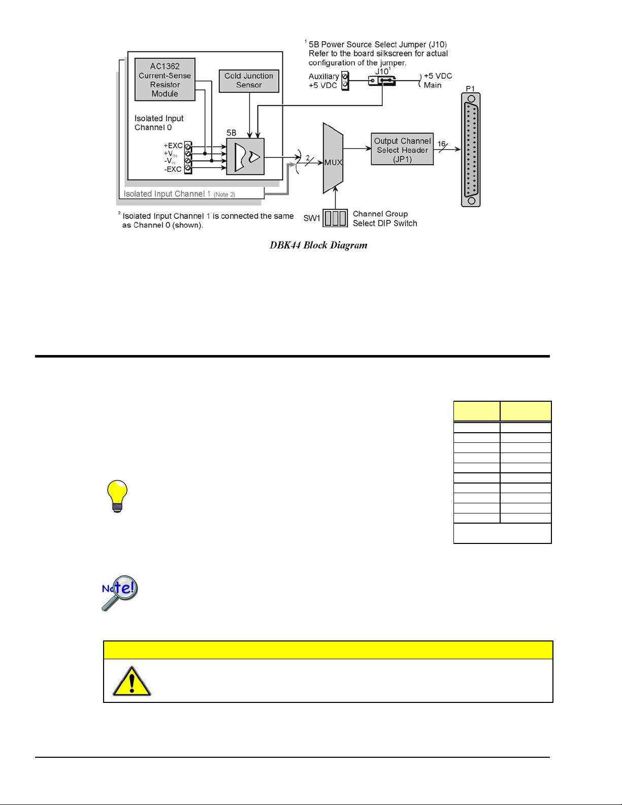
The LogBook or Daq device scans the DBK44’s channels at the same 10 µs/channel rate as other DBKs
(256 scans in 2.56 ms in a full system). Each user-installed 5B module offers 500 V isolation from the
system and between channels. The DBK44 has convenient screw-terminal blocks for signal inputs and
excitation outputs (for use with a strain gage or RTD). Cold junction compensators (CJC) are installed and
ready to use with thermocouple 5B modules. Sockets are provided for AC1362 current-sense resistor
modules.
Hardware Setup
Power Considerations
The DBK44 requires +5 and ±15 VDC from a LogBook, Daq device P1
connector, or auxiliary power supply. In some applications, the DBK44 can draw
enough power from the LogBook’s internal power supply via the P1 connector.
However, the 5B power requirements (+5 VDC only) may be greater than the
LogBook or DaqBook/DaqBoard can provide (see table).
For applications with more than 4 channels, it may be better to use
the DBK42 instead of the DBK44. The DBK42 is a 16-channel
module with a built-in power supply.
External power can be obtained from any regulated 5 V source or from a
TR-4 power supply. External power attaches to the DBK44 via onboard
screw-terminal connections (the Auxiliary Power Input J9 Combicon
terminal at the rear of the board).
5B
Model
5B30 30 mA
5B31 30 mA
5B32 30 mA
5B34 30 mA
5B37 30 mA
5B38 200 mA
5B39 *170 mA
5B40 30 mA
5B41 30 mA
5B47 30 mA
* Maximum output load
resistance is 750 Ω
Current
Required
The 5B38 series strain-gage modules with excitation output require an external power
source. Auxiliary power is also necessary in systems equipped with more than one DBK44.
Prior to using auxiliary power, you must select AUXL on the Power Source Select Jumper
(J10).
CAUTION
DBK44, pg. 2 877095 DBK Option Cards and Modules
Auxiliary power input must not exceed +5 VDC. DBK44 does not regulate auxiliary
power input.
Page 63
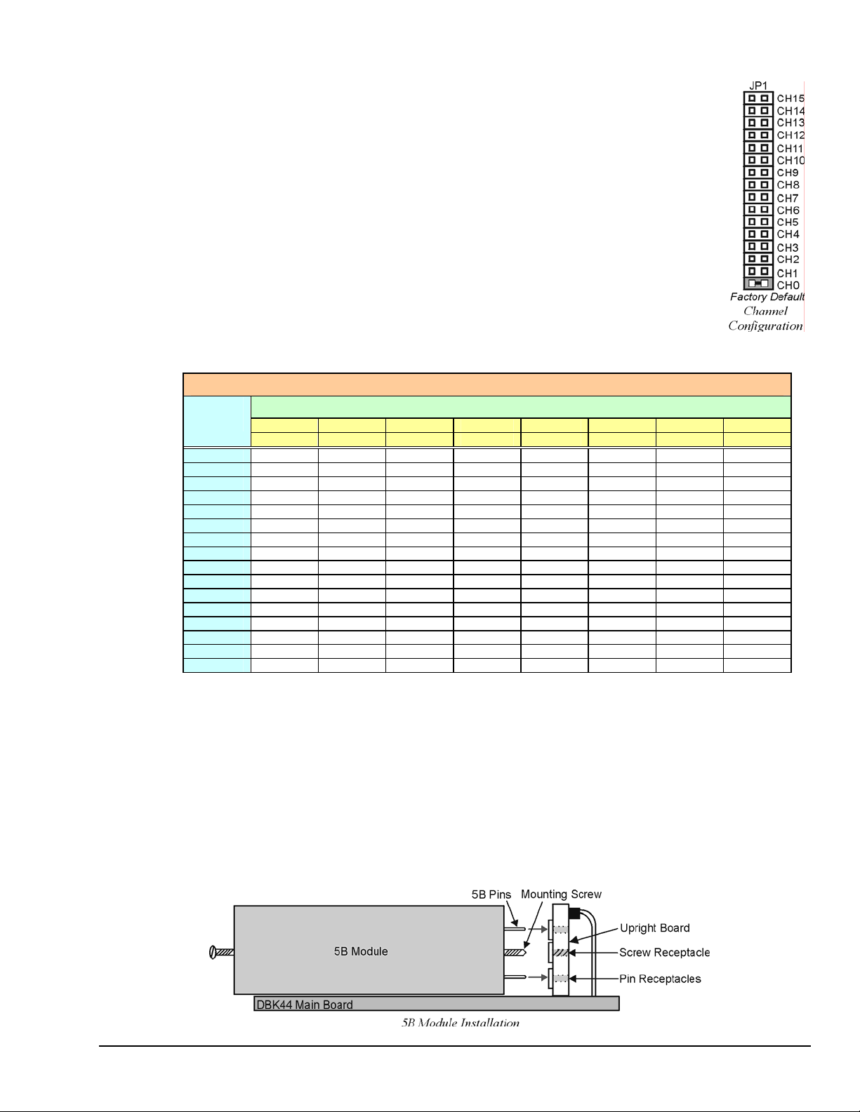
Card Configuration
Up to 128 DBK44s may connect to a LogBook or a Daq device system. Since this is a
daisy-chain interface, each module must appear unique and use a different analog input
channel. To configure the card’s channel, you must set the JP1 jumper and the
SW1 DIP switch to your chosen channel as follows.
1. Locate the 16×2-pin header (labeled JP1) near the front of the card. Note the
16 jumper locations labeled CH0 through CH15 to match the main channel.
2. Place the JP1 jumper on the channel you wish to use. Only one jumper is
used per card, but up to 8 DBK44s can occupy one main channel and use the
same JP1 setting (but with different SW1 settings).
3. Locate the SW1 DIP switch that serves as a channel group select switch and
can distinguish up to 8 cards on a channel.
4. Place the 3 mini switches (CBA) in the position that corresponds to your
chosen channel as shown in the table below. For each JP1 setting, there
are 8 possible SW1 settings to allow two input channels per card).
Channel Pair Determined by JP1 and SW1
JP1
Jumper
CH0 16-17 18-19 20-21 22-23 24-25 26-27 28-29 30-31
CH1 32-33 34-35 36-37 38-39 40-41 42-43 44-45 46-47
CH2 48-49 50-51 52-53 54-55 56-57 58-59 60-61 62-63
CH3 64-65 66-67 68-69 70-71 72-73 74-75 76-77 78-79
CH4 80-81 82-83 84-85 86-87 88-89 90-91 92-93 94-95
CH5 96-97 98-99 100-101 102-103 104-105 106-107 108-109 110-111
CH6 112-113 114-115 116-117 118-119 120-121 122-123 124-125 126-127
CH7 128-129 130-131 132-133 134-135 136-137 138-139 140-141 142-143
CH8 144-145 146-147 148-149 150-151 152-153 154-155 156-157 158-159
CH9 160-161 162-163 164-165 166-167 168-169 170-171 172-173 174-175
CH10 176-177 178-179 180-181 182-183 184-185 186-187 188-189 190-191
CH11 192-193 194-195 196-197 198-199 200-201 202-203 204-205 206-207
CH12 208-209 210-211 212-213 214-215 216-217 218-219 220-221 222-223
CH13 224-225 226-227 228-229 230-231 232-233 234-235 236-237 238-239
CH14 240-241 242-243 244-245 246-247 248-249 250-251 252-253 254-255
CH15 256-257 258-259 260-261 262-263 264-265 266-267 268-269 270-271
CBA CBA CBA CBA CBA CBA CBA CBA
0 0 0 0 0 1 0 1 0 0 1 1 1 0 0 1 0 1 11 0 1 1 1
5B Module Connection
Each input of the DBK44 is processed through a user-installed 5B signal-conditioning module. Different
5B modules are used with different transducer and signal sources. To install the modules:
1. Remove all power from the DBK44.
SW1 DIP Switch Setting
2. Match the footprint of the module with the footprint on the circuit board (see figure).
3. Gently place the module into the footprint, and screw it down.
4. Record the channel the module was placed in.
DBK Option Cards and Modules 877095 DBK44, pg. 3
Page 64
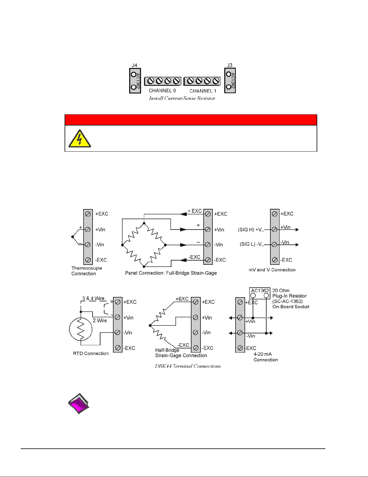
When installing current input modules (SC-5B32 series), be sure to install the current-sense resistor
(SC-AC-1362 shipped with the SC-5B32) in the resistor socket (J4 for ch 0, J3 for ch 1) near the input
screw-terminal block (see figure).
Terminal Block Connection
Input signals (and excitation leads) must be wired to the DBK44 via the 4-contact terminal blocks at the
end of the card. These terminal blocks connect internally to their corresponding signal conditioning
module. The terminal blocks accept up to 14-gage wire into quick-connect screw terminals that are labeled
as to their function. Each type of input signal or transducer (such as a thermocouple or strain gage) should
be wired to its terminal block as shown in the figure. Wiring is shown for RTDs, thermocouples, 20 mA
circuits, mV/V connections, and for full- and half-bridge strain gages.
Shock Hazard! De-energize circuits connected to the DBK44 before changing the
wiring or configuration. The DBK44 is designed to sense signals that may carry
dangerous voltages.
WARNING
P1 Connection
Reference Notes:
Chapter 2 includes pinouts for P1, P2, P3, and P4. Refer to pinouts applicable to your
system, as needed.
The DBK44 attaches to the LogBook’s or Daq Device’s P1 analog I/O connector. Connect the CA-37-x
accessory ribbon cable (with x indicating the number of cards to be connected) from P1 to the DB37
connector at the end of the DBK44 card.
DBK44, pg. 4 877095 DBK Option Cards and Modules
Page 65
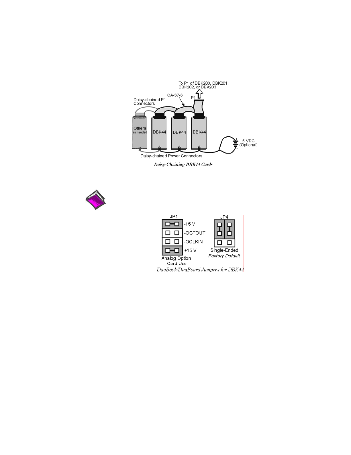
Note: A series of interface cables are available to connect up to 128 DBK44s. You can also use a DBK41
DBK44 can be connected to the P1 connector of DBK200, DBK201, DBK202, or DBK203. Connect the
CA-37-x accessory ribbon cable (with x indicating the number of cards to be connected) from P1 to the
DB37 connector at the end of the DBK44 card.
Note: Interface cables are available to connect up to 128 DBK44s.
CE Compliance
10-slot expansion chassis.
Reference Notes:
Should your data acquisition system need to comply with CE standards, refer to
the CE Compliance section of the chapter Signal Management.
DaqBook/100 Series & /200 Series and DaqBoard [ISA type] Configuration
The DBK44 requires two setup steps in DaqBooks/100 Series & /200 Series devices and
DaqBoards [ISA type]—jumpers JP1 and JP4.
1. If not using auxiliary power, ensure the JP1 jumper is configured for Analog Option Card Use
(expanded analog mode).
Note: This default position is necessary to power the interface circuitry of the DBK44 via the
internal ±15 VDC power supply. If using auxiliary power from a DBK32A or DBK33 card,
you must remove both JP1 jumpers. Refer to Power Requirements in the DBK Basics section.
Also refer to the DBK32A and DBK33 sections as applicable.
2. For DaqBook/100, /112, and /120 only, place the JP4 jumper in the DaqBook or DaqBoard [ISA
type] in single-ended mode. Note that analog expansion cards convert all input signals to single-
ended voltages referenced to analog common.
Note: The configuration of the JP3 jumper depends on the output range of the 5B module. For
example, a 5B31 volt input module has an output range of -5 to +5 V in bipolar mode. A
5B47 T/C module (output 0 to +5 V) could use bipolar mode, but unipolar mode is more
appropriate.
DBK Option Cards and Modules 877095 DBK44, pg. 5
Page 66

DaqBook/2000 Series and DaqBoard/2000 Series Configuration
No jumper configurations are required for these 2000 series devices.
Software Setup
Reference Notes:
o DaqView users - Refer to chapter 3, DBK Setup in DaqView.
o LogView users - Refer to chapter 4, DBK Setup in LogView.
DBK44, pg. 6 877095 DBK Option Cards and Modules
Page 67
mx+b Values for 5B Modules
The mx+b calculations for most 5B modules are included within LogView software. The table shows the
m and b values for various 5B modules.
5B Module m Value b Value Engineering
Isolated Voltage Input (5 V Current Requirement, 30 mA)
SC-5B31-01 1/5 0 mV, V
SC-5B31-02 1 0 mV, V
SC-5B31-03 2 0 mV, V
SC-5B31-04 2/5 -1 mV, V
SC-5B31-05 2 -5 mV, V
SC-5B31-06 4 -10 mV, V
Isolated Wideband Voltage (5 V Current Requirement, 30mA)
SC-5B41-01 1/5 0 V
SC-5B41-02 1 0 V
SC-5B41-03 2 0 V
SC-5B41-04 2/5 -1 V
SC-5B41-05 2 -5 V
SC-5B41-06 4 -10 V
Isolated Millivolt Input (5 V Current Requirement, 30 mA)
SC-5B30-01 2 0 mV
SC-5B30-02 10 0 mV
SC-5B30-03 20 0 mV
SC-5B30-04 4 -10 mV
SC-5B30-05 20 -50 mV
SC-5B30-06 40 -100 mV
Isolated Wideband Millivolt (5 V Current Requirement, 30 mA)
SC-5B40-01 2 0 mV
SC-5B40-02 10 0 mV
SC-5B40-03 20 0 mV
SC-5B40-04 4 -10 mV
SC-5B40-05 20 -50 mV
SC-5B40-06 40 -100 mV
Isolated Linearized T/C Input (5 V Current Requirement, 30 mA)
SC-5B47-J-01 152 0 °C
SC-5B47-J-02 80 -100 °C
SC-5B47-J-03 100 0 °C
SC-5B47-K-04 200 0 °C
SC-5B47-K-05 100 0 °C
SC-5B47-T-06 100 -100 °C
SC-5B47-T-07 40 0 °C
SC-5B47-E-08 200 0 °C
SC-5B47-R-09 250 +500 °C
SC-5B47-S-10 250 +500 °C
SC-5B47-S-11 260 +500 °C
Isolated RTD Input (5 V Current Requirement, 30 mA)
SC-5B34-01 40 -100 °C
SC-5B34-02 20 0 °C
SC-5B34-03 40 0 °C
SC-5B34-04 120 0 °C
SC-5B34-C-01 24 0 °C
SC-5B34-C-02 24 0 °C
SC-5B34-N-01 24 0 °C
Isolated Current Input (5 V Current Requirement, 30 mA)
SC-5B32-01 3.2 4 mA
SC-5B32-02 4 0 mA
Voltage Switch Input
SC-AC-1367 1 0 V
Unit(s)
DBK Option Cards and Modules 877095 DBK44, pg. 7
Page 68

DBK44 – Specifications
Name/Function: 2-Channel 5B Signal Conditioning Card
Module Capacity: 2 “input only” 5B modules
Weight: 0.25 kg (8 oz.) with no modules installed
Cable (optional): CA-37-x
DC Input Fuse: 4 A
Connections:
Male DB37 mates via CA-37-1 cable with P1 on the LogBook,
DaqBook, ISA-type DaqBoard*, or Daq PC-Card.
User connections include 8 screw-terminals (4 per channel).
Screw terminations, per channel, are: +EXC, +Vin, -Vin, -EXC
Isolation to Primary Acquisition Device (LogBook or Daq Device):
Input Power: 0 VDC
Signal Inputs: 1500 VDC
Input Channel-to-Channel: 500 VDC
Environmental:
Operating Temperature: 0 to 50°C
Humidity: 0 to 80% RH @ 30°C; de-rate 3%/°C
Altitude: 0 to 2000 m
*Note: For DaqBoard/2000 Series and /2000c Series boards, the use of a
DBK200 Series P4-to-P1 adapter is required.
DBK44, pg. 8 877095 DBK Option Cards and Modules
Page 69
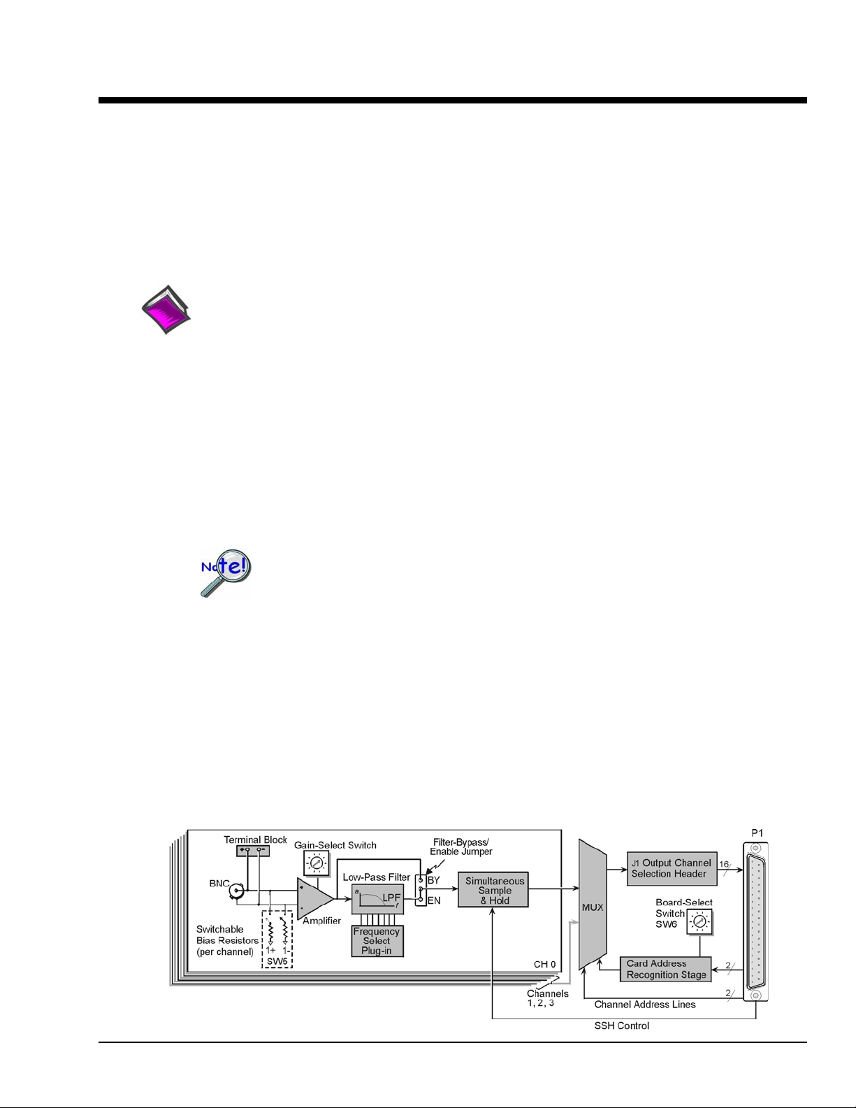
DBK45 4-Channel SSH and Low-Pass Filter Card
Overview …… 1
Hardware Setup …… 2
Card Connection …… 2
Card Configuration …… 2
Configuring DBK45 Filter Sections …… 3
DaqBook/100 Series & /200 Series and DaqBoard [ISA type] Configuration …… 5
DaqBook/2000 Series and DaqBoard/2000 Series Configuration …… 5
Software Setup …… 5
DBK45 – Specifications …… 6
Reference Notes:
o Chapter 2 includes pinouts for P1, P2, P3, and P4. Refer to pinouts applicable to your
Overview
The DBK45 combines the features of the DBK17 (SSH) and the DBK18 (low-pass filter) cards. Each
DBK45 provides 4 input channels to a LogBook or Daq device system. Each of the main 16 analog input
channels can accept four DBK45s, for a maximum of 64 DBK45s and 256 analog input channels. The
simultaneous sample-hold function is activated at the beginning of each channel scan and freezes all
signals present on DBK45 inputs for the duration of the scan, allowing for non-skewed readings of all
channels.
system, as needed.
o In regard to calculating system power requirements, refer to DBK Basics located near
the front of this manual.
You should never set a DBK45 channel as the 1st channel in a scan due to timing of
the SSH line.
For each of the four channels, a separate filter and a sample-hold stage follow the input stage. The outputs
are connected to a 4-channel multiplexer stage. The enabled-output MUX allows four DBK45s to share a
common analog input channel.
The DBK45 has an instrumentation amplifier for each channel, with switch-selected gains of ×1, ×10,
×100, ×200 and ×500. A socket is provided for a gain resistor for custom gain-selection instead of the 5
factory-default gains. Gain for any channel can be set to any value between unity and ×500 by installing
an appropriate resistor. Four separate filter stages follow the 4 input stages. The outputs are connected to
a
4-channel multiplexer stage. The enabled output MUX allows four DBK45s to share a common analog
base channel.
Input can be connected to a channel’s BNC or terminal block connector. The differential inputs are
provided with switchable 100 kΩ bias resistors to analog common.
DBK Option Cards and Modules 987696 DBK45, pg. 1
Page 70
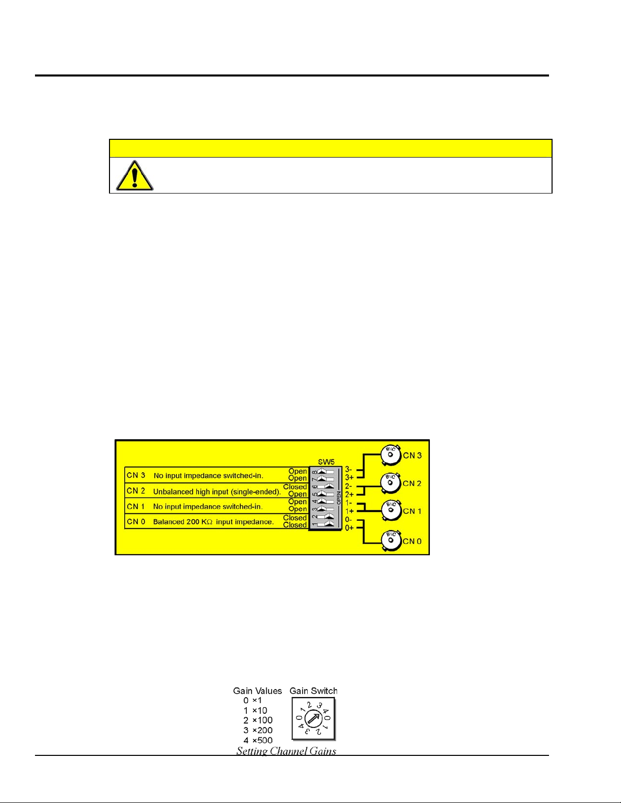
Hardware Setup
Card Connection
DBK45 Block Diagram
DBK45 is equipped with a BNC connector for each of the four differential analog inputs. The card
includes terminal block connections, which can be used instead of the BNC connectors if desired.
Card Configuration
Factory Defaults:
Input Termination
DBK45 provides two 100 KΩ bias resistors for each analog input. For balanced 200 KΩ input
impedance, both resistors should be switched in. An 8-position DIP switch (SW5) can selectively engage
the bias resistors. The switches must be in the closed position to engage the termination resistors. For
unbalanced high input, only the (-) resistor should be used. If neither resistor is used, some external bias
current path is required. Examples of SW5 switch positions and the resulting impedance selection
follows.
CAUTION
Input voltage levels must not exceed ±5 V bipolar or 10 V unipolar.
• 100K bias resistors – Enabled
• Low pass filter – Disabled (bypassed)
• Gain – x1
• SSH - Enabled
Examples of Bias Resistor Selection Options
Gain Settings
On the printed circuit board, each channel has one gain-set switch. The switches are labeled GAIN 1,
GAIN 2, GAIN3, and GAIN 4. Each channel also has holes in the board for gain resistors labeled RG1 to
RG4. The 5 gain values for switch settings 0 to 4 are provided in the following figure. If a custom gain is
desired, the switch is set to position 0; and a gain resistor must be mounted and soldered onto the board.
The gain resistor’s value is determined by the formula: R
DBK45, pg. 2 987696 DBK Option Cards and Modules
= [40,000 / (Gain -1)] - 50 Ω
GAIN
Page 71
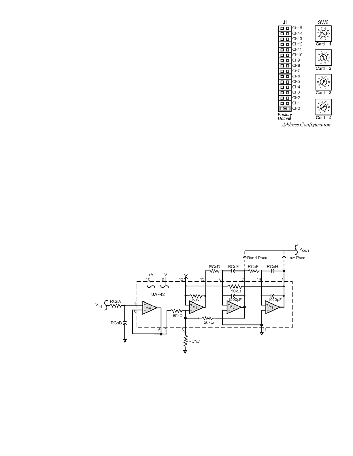
Address Configuration
Up to four DBK45s can be connected to each analog channel. With
16 main channels and 4 inputs per DBK45, 256 inputs are possible. Since this is
a daisy-chain interface, each DBK45 must have a unique address (channel and
card number). Note that the default setting of SW6 is Card 1.
To configure the module, locate the 16 × 2-pin header (labeled J1) near the front
of the board (near P1). The 16 jumper locations on this header are labeled CH0
through CH15. Place the jumper on the channel you wish to use. Only one
jumper is used.
Note: Two DBK45s in the daisy-chain can have the same channel number as
long as their card number is unique.
Set switch SW6 for each DBK45 on a single channel. Verify that only one card
in the system is set to a particular channel and card number.
Configuring DBK45 Filter Sections
There are 4 low-pass, 3-pole active filters on the DBK45. Each filter can be enabled (EN) or bypassed
(BY) by placement of the jumper on J3 for channel 0, J4 for channel 1, J5 for channel 2, J6 for
channel 3. The factory-default setting is enabled (EN) for each channel. Each filter can be configured as
a Butterworth, Bessel, or Chebyshev filter with corner frequencies up to 50 kHz. Filter properties depend
on the values of resistors and capacitors installed in several circuit locations. Above 10 Hz, installing
capacitors is unnecessary because capacitors in the ICs are sufficient. In all cases, three resistors are
required to complete the active filter circuits contained mostly within the UAF42 ICs.
The following circuit diagram shows the active filter IC in a typical section of the DBK45. The resistors
and capacitors outside the IC have a physical location in a DIP-16 socket (dual in-line, 16 pins) with an
RCnn designator. The RC indicates the needed part is a resistor or capacitor; the 3rd character is the
channel number; and the 4th character corresponds to the socket position (A-H).
Filter Circuit Diagram
A machined-pin IC socket in each filter RC location can accept resistors and capacitors that plug directly
into the socket; however, this is not recommended. Two much better approaches exist. The first is to use
pre-configured plug-in filter modules; the second is to configure your own plug-in module using a blank
CN-115. Both of these options are illustrated on the following page.
The use of plug-in modules provides excellent “gold-to-gold” contact between the components of the plugin module and the on-board header.
DBK Option Cards and Modules 987696 DBK45, pg. 3
Page 72
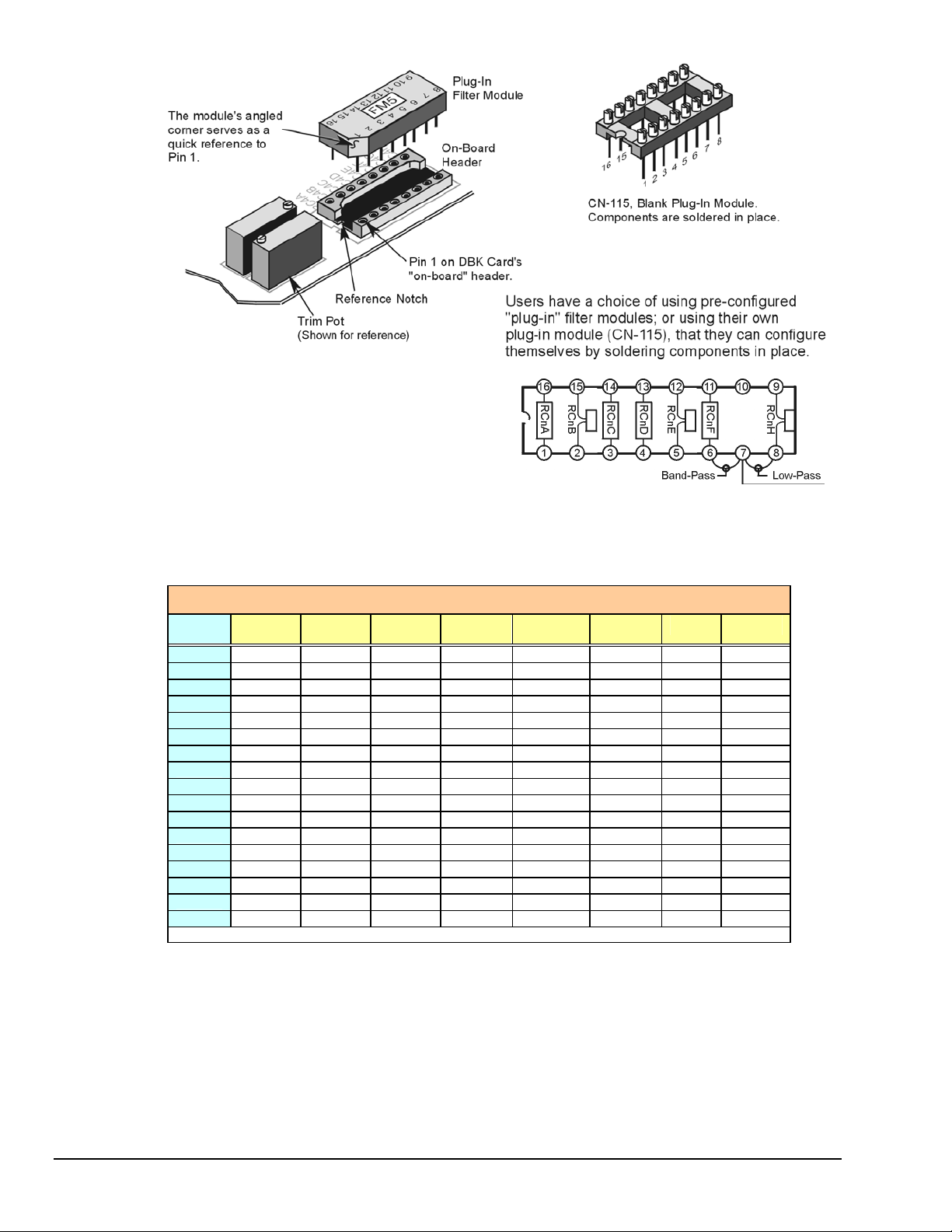
The right-hand figure shows the DIP-16
component pattern typical of the 4 filter sections.
Note: “n” corresponds to “channel number.”
Pin 7 of the DIP-16 socket:
• connects to pin 8 for low-pass filtering
• connects to pin 6 for band-pass filtering
DIP-16 Component Pattern
The following table lists values of components for common corner frequencies in Butterworth filters. If
designing your own filter, software from Burr-Brown provides the component values to create the desired
filter. Note that the design math is beyond the scope of this manual.
3-Pole Butterworth Filter Components
3dB
(Hz)
0.05
0.10
0.20
0.50
1
2
5*
10*
20
50
100*
200
500*
1000*
2000
5000
10000
*These pre-configured Butterworth frequency modules are available from the manufacturer.
RCnA RCnB RCnC RCnD RcnE RCnF RCnG RCnH
3.16 MΩ
1.58 MΩ
787 kΩ
3.16 MΩ
1.58 MΩ
787 kΩ
3.16 MΩ
1.58 MΩ
787 kΩ
3.16 MΩ
1.58 MΩ
787 kΩ
316 kΩ
158 kΩ
78.7 kΩ
31.6 kΩ
15.8 kΩ
1 µF none
1 µF none
1 µF none
0.1 µF none
0.1 µF none
0.1 µF none
0.01 µF none
0.01 µF none
0.01 µF none
0.001 µF none
0.001 µF none
0.001 µF none
0.001 µF none
0.001 µF none
0.001 µF none
0.001 µF none
0.001 µF none
3.16 MΩ
1.58 MΩ
787 kΩ
3.16 MΩ
1.58 MΩ
787 kΩ
3.16 MΩ
1.58 MΩ
787 kΩ
3.16 MΩ
1.58 MΩ
787 kΩ
316 kΩ
158 kΩ
78.7 kΩ
31.6 kΩ
15.8 kΩ
1 µF
1 µF
1 µF
0.1 µF
0.1 µF
0.1 µF
0.01 µF
0.01 µF
0.01 µF
none
none
none
none
none
none
none
none
3.16 MΩ
1.58 MΩ
787 kΩ
3.16 MΩ
1.58 MΩ
787 kΩ
3.16 MΩ
1.58 MΩ
787 kΩ
3.16 MΩ
1.58 MΩ
787 kΩ
316 kΩ
158 kΩ
78.7 kΩ
31.6 kΩ
15.8 kΩ
none 1 µF
none 1 µF
none 1 µF
none 0.1 µF
none 0.1 µF
none 0.1 µF
none 0.01 µF
none 0.01 µF
none 0.01 µF
none none
none none
none none
none none
none none
none none
none none
none none
You have the option to configure the filter sections as b and-pass filters rather than low-pass filters. The
component selection program provides band-pass component values. The program also computes and
displays phase and gain characteristics of the filter sections as a function of freq uency.
DBK45, pg. 4 987696 DBK Option Cards and Modules
Page 73
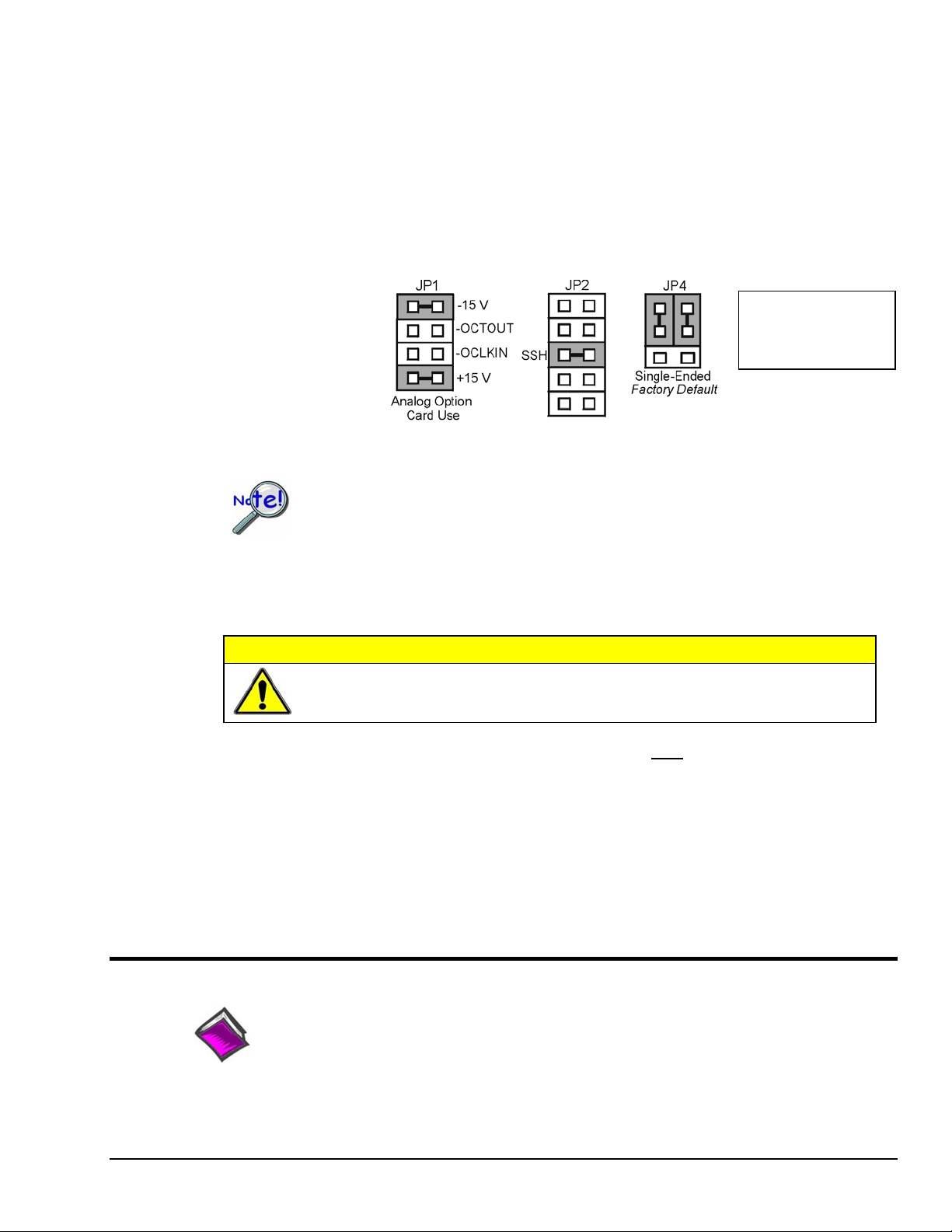
DaqBook/100 Series & /200 Series and DaqBoard [ISA type] Configuration
Use of the DBK45 requires setting jumpers in DaqBooks/100 Series & /200 Series devices and
ISA-type DaqBoards.
1. If not using auxiliary power, set the JP1 jumper for Analog Option Card Use (also referred to
as Analog Expansion Mode).
Note:
These jumpers do not
apply to /2000 Series
devices.
Jumpers on DaqBook/100 Series, DaqBook/200 Series, and ISA-type DaqBoards
The JP1 default position (Analog Option Card Use) is necessary to power the interface
circuitry of the DBK45 via the internal ±15 VDC power supply. If using auxiliary
power, e.g., DBK32A or DBK33, you must remove both JP1 jumpers. Refer to
Power Requirements in the DBK Basics section and the DBK32A and DBK33 sections for
more information, as applicable.
2. Place the JP2 jumper in the SSH position.
Do not use an external voltage reference for DAC1. Applying an external voltage
CAUTION
reference for DAC1, when using the SSH output, will result in equipment damage
due to a conflict on P1, pin #26.
3. For DaqBook/100, DaqBook/112 and DaqBook/120
only, place the JP4 jumper in
single-ended mode.
DaqBook/2000 Series and DaqBoard/2000 Series Configuration
No hardware configuration is required for DaqBook/2000 Series or DaqBoard/2000 Series devices.
Software Setup
Reference Notes:
o DaqView users - Refer to chapter 3, DBK Setup in DaqView.
o LogView users - Refer to chapter 4, DBK Setup in LogView.
DBK Option Cards and Modules 987696 DBK45, pg. 5
Page 74

DBK45 – Specifications
Name/Function: Simultaneous Sample and Hold and
Low-Pass Filter Card
Number of Channels: 4
Input Connections: 4 BNC connectors; 4 screw-terminal sets
Output Connector: DB37 male,
mates with P1 using CA-37-x cable
Number of Cards Addressable: 64
Dimensions: 8.25” × 3.25”
Input Type: Differential
Voltage Input Ranges:
0 to ±5000 mVDC
0 to ±500 mVDC
0 to ±50 mVDC
0 to ±25 mVDC
0 to ±10 mVDC
For Custom Gains: R
Input Amplifier Slew Rate: 12 V/µs minimum
Acquisition Time:
0.6 µs (10 V excursion to 0.1%)
0.7 µs (10 V excursion to 0.01%)
Channel-to-Channel Aperture Uncertainty: 50 ns
Output Droop Rate: 0.1 µV/µs
Input Gains: ×1, ×10, ×100, ×200, x500, and
user-set up to ×500
Input Offset Voltage: 500 µV + 5000/G maximum (nullable)
Input Offset Drift: ±5 + 100/G µV/°C maximum
Input Bias Current: 100 pA maximum
Input Offset Currents: 50 pA maximum
Input Impedance: 5 × 10
Switchable Bias Resistors: 100 KΩ each to analog common
= [40,000/(Gain-1)] - 80 Ω
GAIN
12
Ω parallel with 6 pF
Gain Errors:
0.04% @ ×1
0.1% @ ×10
0.2% @ ×100
0.4% @ ×200
1.0% @ ×500
Temperature vs Gain:
±20 ppm/°C @ ×1
±20 ppm/°C @ ×10
±40 ppm/°C @ ×100
±60 ppm/°C @ ×200
±100 ppm/°C @ ×500
Non-Linearity:
±0.015 % full-scale @ ×1
±0.015 % full-scale @ ×10
±0.025 % full-scale @ ×100
±0.025 % full-scale @ ×200
±0.045 % full-scale @ ×500
Common-Mode Rejection:
70 dB minimum @ ×1
87 dB minimum @ ×10
100 dB minimum @ ×100
100 dB minimum @ ×200
100 dB minimum @ ×500
Active Filter Device: UAF42 (Burr-Brown)
Number of Poles/Filter: 3
Types of Filters: Bessel, Butterworth,
Chebyshev
Frequency Range: 0.1 Hz to 50 kHz
The frequency is set by installation of
4-6 resistors and/or capacitors in
provided socket locations.
Frequency Modules: Optional frequency
module kits are available that consist of
4 plug-in resistor/capacitor (RC)
headers. These RC headers are preconfigured for any of the following
frequencies: 5 Hz, 10 Hz, 100 Hz,
500 Hz, or 1 kHz—all are Butterworthtype filters.
DBK45, pg. 6 987696 DBK Option Cards and Modules
Page 75
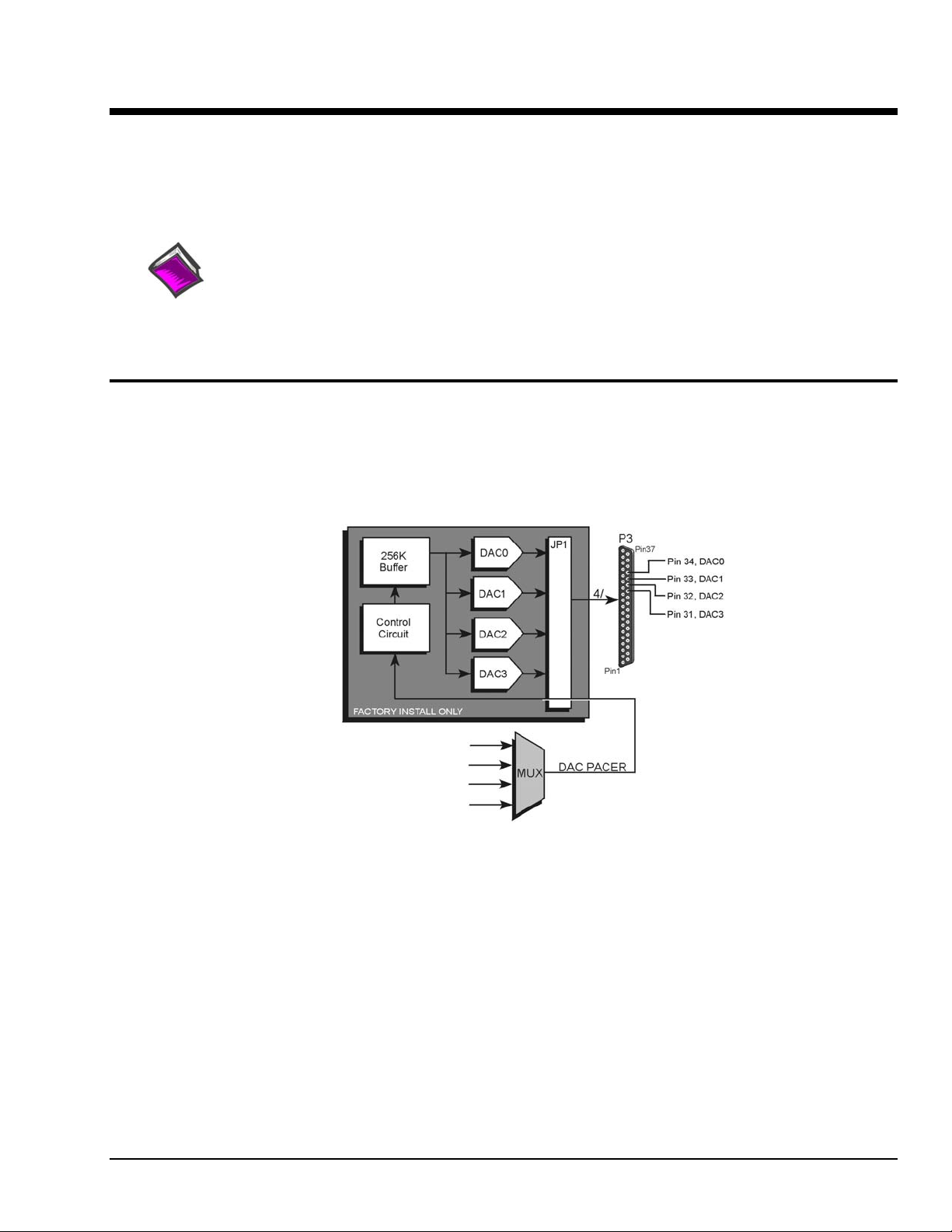
DBK46 4-Channel Analog Output Card
Daq
Overview
Overview ...... 1
Hardware Setup ...... 3
Software Setup ...... 3
For use with: DaqBook/2000A
DaqBook/2000E
DaqBook/2000X
DBK46 – Specifications ......4
Reference Notes:
o Chapter 2 includes pinouts for P1, P2, P3, and P4. Refer to pinouts applicable to your
system, as needed.
o The P3 connector’s DAC related pins [31, 32, 33, and 34] apply to the DaqBook/2000 Series
Device only when a DBK46 is installed. For WBK41, DAC related connections are made via
a front panel screw terminal block.
The DBK46 is a factory-installed option currently available for DaqBook/2000A, DaqBook/2000E,
DaqBook/2000X, and WBK41. JP1 plugs into a 40-pin header on the primary acquisition device.
Analog DAC Output is then available, as follows:
•
For DaqBook/2000 Series devices, from the device’s P3 connector.
•
For WBK41, from a front panel terminal block.
WBK41
The 37-pin P3 connector is
on the DaqBook/2000
Internal Acquisition Pacer Clock
External Acquisition Pacer Clock
Pin 20 on P1; Pin B26 on P4
Internal DAC Pacer Clock
External DAC Pacer Clock
Pin 21 on P3; Pin A26 on P4
Series device front panel.
DBK46 Block Diagram,
Book/2000 Series Applications
DBK Option Cards and Modules 967194 DBK46, pg. 1
Page 76
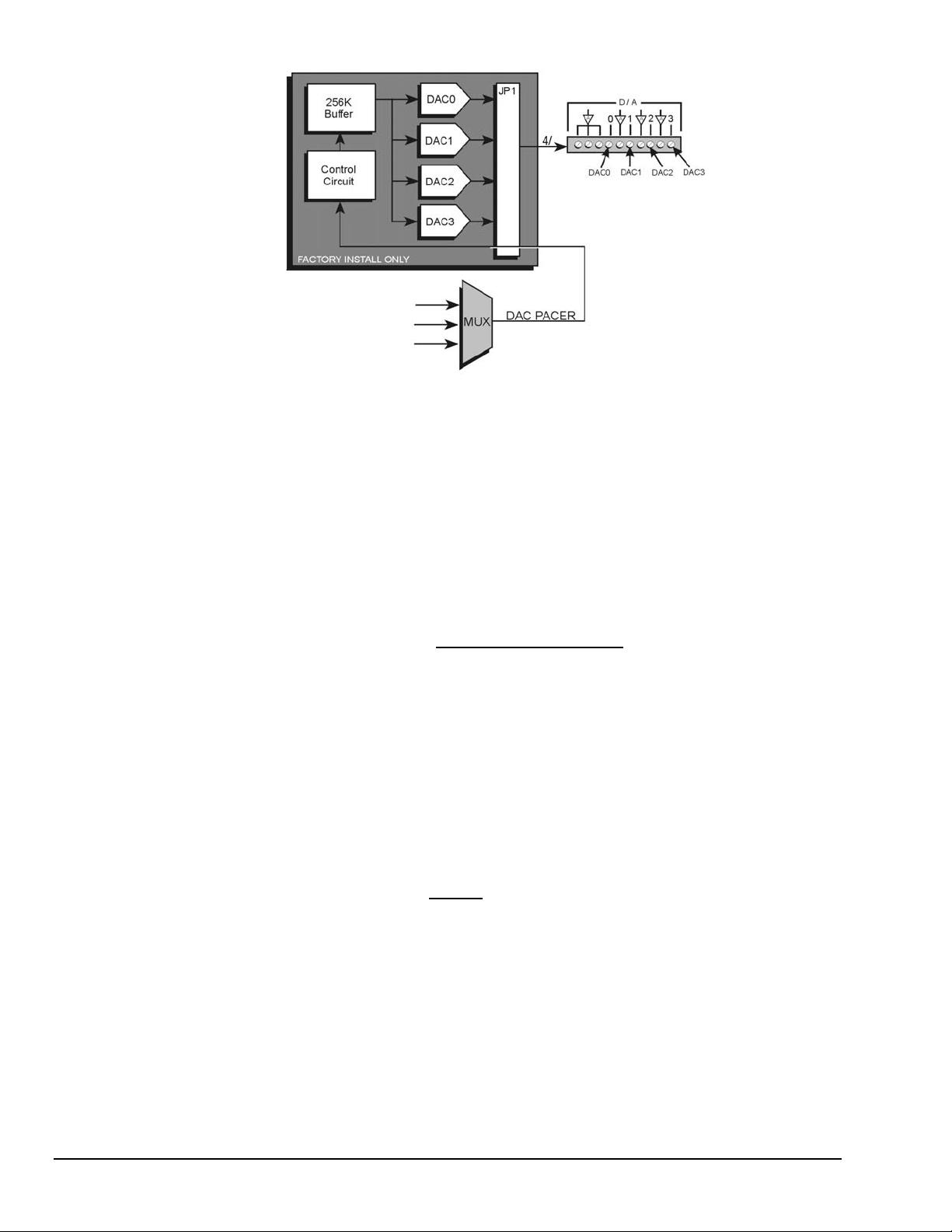
WBK41 Front Panel,
Right-Edge Terminal Block
Internal DAC Pacer Clock
Internal Acquisition Pacer Clock
External DAC Pacer Clock (DPCR)
DBK46 Block Diagram,
WBK41 Application
The DBK46 has a 256K sample buffer that can be used for one to four DACs. If only one DAC is enabled
for waveform output, then the entire 256K sample memory can be used to store a waveform for that DAC.
If two DACs are enabled for waveform output, then 128K of sample memory is available for each of the
two DACs. Use of all four DACs drops the available memory down to 64K per DAC.
Software loads the waveform(s) into all, or a portion of, the 256K sample buffer. The waveform data
drives the DACs at the rate of the specified DAC Pacer Clock. The waveforms will repeat until the DACs
are disabled by software.
The DBK46 provides an output range of -10V to +10V. The card’s 256 Kbyte of sample buffer memory
can store waveforms from the PC.
When used to generate waveforms for a
DaqBook/2000 Series device, each DAC can be independently
clocked in one of four modes. These are:
Internal DAC Pacer Clock - The on-board programmable clock can generate updates ranging
•
from 1.5 Hz to 100 kHz, independent of any acquisition rate.
•
Internal Acquisition Pacer Clock - Using the on-board programmable clock, the analog
output rate of update can be synchronized to the acquisition rate derived from 100 kHz to once
every 5.96 hours.
•
External DAC Pacer Clock - A user-supplied external input clock can be used to pace the
DAC, entirely independent of other analog inputs.
•
External Acquisition Pacer Clock - A user-supplied external input clock can simultaneously
pace the DAC and the analog input.
When used to generate waveforms in a
WBK41, the DACs can be clocked in one of three modes.
These are:
Internal DAC Pacer Clock - The WBK41 programmable clock can generate updates ranging
•
from 1.5 Hz to 100 kHz, independent of any acquisition rate.
DBK46, pg. 2
•
Internal Acquisition Pacer Clock – By using the WBK41 programmable clock, the analog
output rate of update can be synchronized to the acquisition rate derived from 100 kHz to once
every 5.96 hours.
•
External DAC Pacer Clock (DPCR) - A user-supplied external input clock can be used to
pace the DAC, entirely independent of other analog inputs. This external clock input connects
to the DPCR connector, located on the Counter/Timer Terminal Block.
967194 DBK Option Cards and Modules
Page 77

Hardware Setup
DBK46 is installed at the factory. To verify that a DBK46 is installed, simply check the acquisition
software’s Analog Output Window for the presence of DAC0, DAC1, DAC2, and DAC3.
Software Setup
DBK46 does not require setup in software.
Reference Notes:
o DaqView Users: In regard to the out-of-the-box software and analog output channels, refer to the
DaqView and DaqViewXL Document Module, especially the following two sections: Analog Output
Window, and Waveform and Digital Pattern Output Window.
o WaveView Users: In regard to the out-of-the-box software, refer to the WaveView Document
Module.
o PDF versions of the documents are included on the data acquisition CD and can be accessed via the
<View PDFs> button, which is located on the CD’s intro-screen.
DBK Option Cards and Modules 967194 DBK46, pg. 3
Page 78

DBK46 – Specifications
The four analog output channels are updated synchronously relative to scanned inputs, and are clocked
from either an internal clock on the primary acquisition device, such as a DaqBook/2000A; or from a usersupplied external clock source. Analog outputs can also be updated asynchronously, independent of any
other scanning in the system.
Channels: 4
Resolution: 16 bits
Data Buffer: 256 K sample FIFO
Output Voltage Range: ±10V
Output Current: ±10 mA
Offset Error: ±0.0045V max
Gain Error: ±0.01%
Update Rate: 100 kHz max, 1.5 Hz min (no minimum with external clock)
Settling Time: 10 µsec max to 1 LSB for full-scale step
Digital Feed-thru: a spike of up to 50 mV may occur on the DAC output
each time the DAC output is updated
Clock Sources: 4 programmable clock sources:
•
The primary acquisition device’s onboard D/A input clock, independent of the scanning input clock
•
The primary acquisition device’s onboard scanning input clock
An external D/A input clock, independent of an external scanning input clock
•
An external scanning input clock
•
Note: Specifications are subject to change without notice.
DBK46, pg. 4
967194 DBK Option Cards and Modules
Page 79
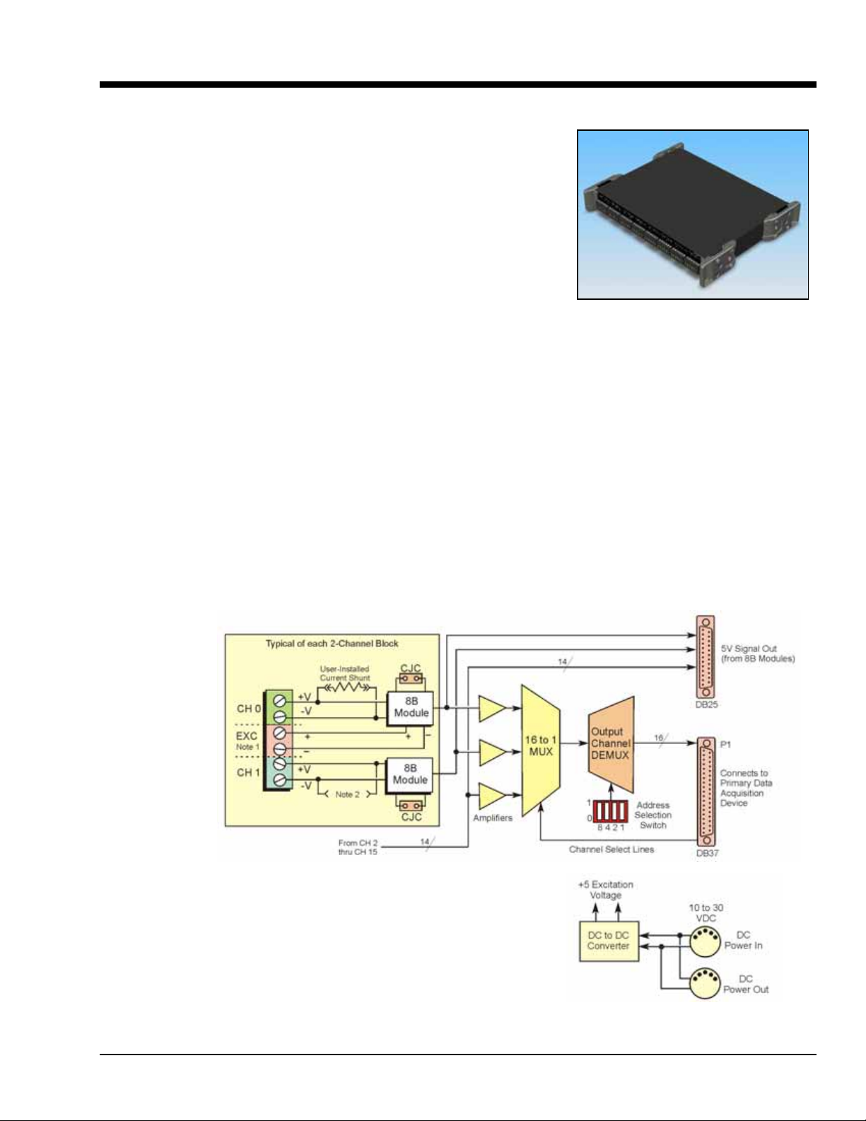
DBK48 Multipurpose Isolated Signal-Conditioning Module
Supports up to Sixteen 8B Modules
Description …… 1
Safety Concerns …… 2
Hardware Setup …… 2
Installing 8B Modules …… 4
Installing Plug-in Resistors to Create 4 to 20 mA Loops …… 5
Making Terminal Block Connections …… 6
Setting DBK48 Module Addresses …… 7
Configuring the Primary Data Acquisition Device …… 8
CE Compliance …… 9
Connecting the DBK48 to the Primary Data Acquisition Device …… 9
Using the DB25 Signal Output Connector …… 10
Powering the System …… 13
Software Setup …… 13
Specifications …… 16
Description
The DBK48 module can accommodate up to sixteen 8B isolated-input signal-conditioning modules for use
with Daq systems. A single cable connects the DBK48 output to the P1 analog input connector on the
primary device. One Daq system can support up to 16 DBK48 modules, providing a total of 256 isolated
analog input channels. The A/D converter scans the DBK48 channels at the same 5 µs/channel rate that it
scans all other channels from DBK series analog expansion and signal conditioning cards.
Other features of DBK48 include:
• Built-in power supply that operates from 10 to 30 VDC and can power a full complement of
8B modules (even with bridge excitation).
• Removable, plug-in screw-terminal blocks for convenient connection of 8B modules.
• On-board cold-junction sensing for thermocouple 8B modules.
• For each 8B module, 250 V isolation from the system and from other channels.
Note 1: Only channels 0, 2, 4, 6, 8, 10, 12, and 14 can be connected
to excitation. For example, in the above block diagram
Channel 0 could be connected to Excitation; Channel 1
could not.
Note 2: Each channel can accept a plug-in resistor to serve as a
8B Isolated Signal Conditioning Module 958893 DK48, pg. 1
current shunt. In the above diagram, Channel 0 has a
current shunt installed, Channel 1 does not. Only currentinput type modules require the plug-in resistors. The plug-in
resistors must be removed for all other module types.
Page 80
Safety Concerns
DBK48 has a 250 VDC isolation specification. This is in a normal environment free of conductive
pollutants and condensation. The 250 VDC rating requires a proper earth ground connection to the chassis
and treatment of adjacent inputs as potentially hazardous.
Input cables must be rated for the isolation potential in use. Line voltage ratings are much lower than the
DC isolation values specified due to transients that occur on power lines. Never remove the cover unless all
inputs with potentially hazardous voltages are removed. The cover must be securely screwed on during
use.
Some things to remember:
WARNING
Shock Hazard! Voltages above 50 Vrms AC and voltages above 100 VDC are
considered hazardous. Safety precautions are required when 8B modules are used in
situations that require high-voltage isolation from the rest of the system. Failure to
practice electrical safety precautions could lead to injury or death.
• Properly tighten all chassis screws before system use.
• Never plug in or unplug potentially hazardous connections with power applied to any
connected equipment.
• Never attempt to change 8B modules or remove the cover plate while power is applied to
the DBK48. You could short out internally exposed circuits and cause personal injury or
equipment damage.
• Disconnect power, all equipment, and signal lines from the DBK48 prior to installing
8B modules.
Reference Note:
Refer to user manual that is associated with your primary Daq device.
DBK48, pg. 2 959893 8B Isolated Signal Conditioning Module
Page 81
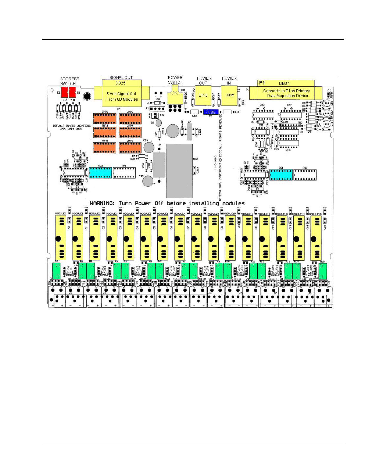
Hardware Setup
DBK48 Circuit Board Layout
8B Isolated Signal Conditioning Module 958893 DK48, pg. 3
Page 82
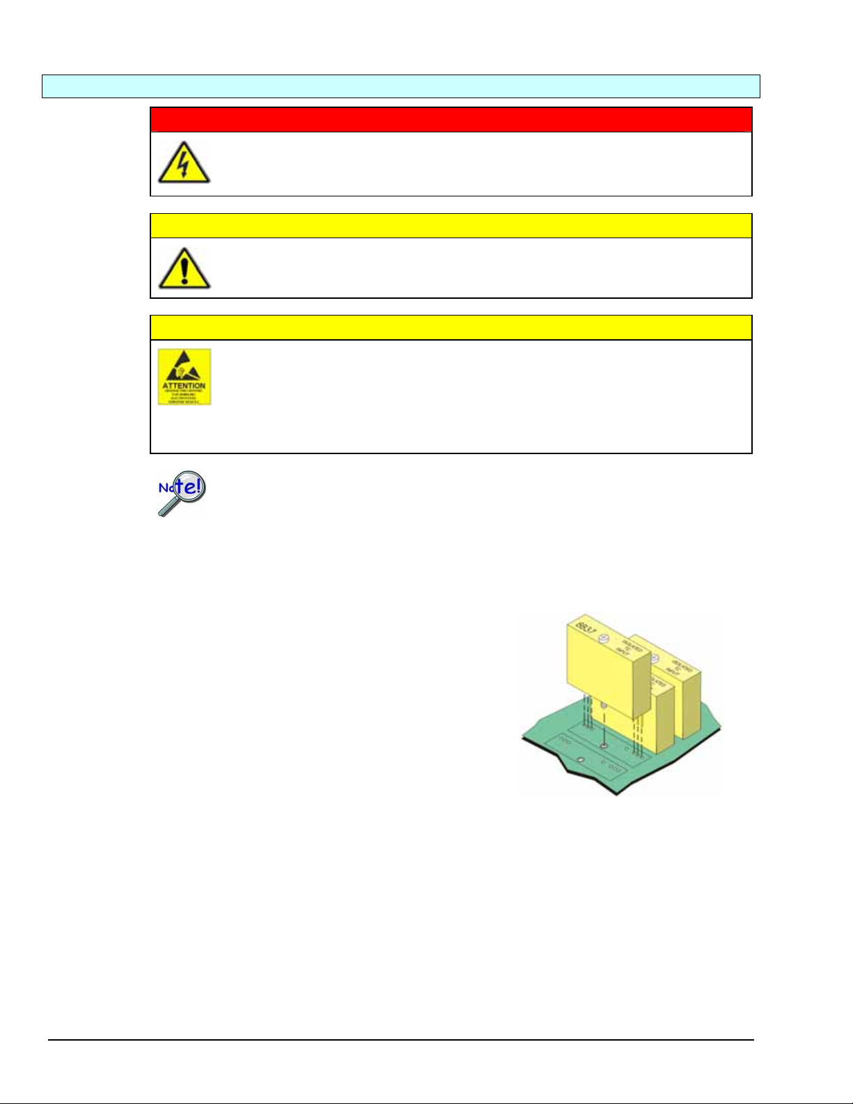
Installing 8B Modules
Electric shock hazard! Turn off power to the DBK48 and all connected modules and
devices before inserting or removing modules. Failure to do so could lead to injury or
death due to electric shock.
CAUTION
WARNING
Handle the 8B module carefully while inserting pins into the circuit board.
Do not over-tighten the mounting screw.
CAUTION
The discharge of static electricity can damage some electronic components.
Semiconductor devices are especially susceptible to ESD damage. You should always
handle components carefully, and you should never touch connector pins or circuit
components unless you are following ESD guidelines in an appropriate ESD
controlled area. Such guidelines include the use of properly grounded mats and wrist
straps, ESD bags and cartons, and related procedures.
If the DBK48 is not connected to a Daq device via the P1 connector, then remove the
Rnets from S01 and S02. These resistor networks connect each 8B module’s output to
the multiplexer for P1.
Up to sixteen 8B modules can be installed onto the DBK48 circuit board. The preceding figure indicates
module locations.
To install 8B modules:
1. Turn off power to the DBK48 and all
connected modules and devices.
2. Disconnect power, all equipment, and signal
lines from the DBK48 prior to installing 8B
modules. Be aware that isolated
measurements can present lethal voltages!
3. Remove the DBK48 top cover plate and set aside.
4. Align the 8B module’s retaining screw and pins
with the holes in the circuit board (see figure).
5. Gently press the module into place.
6. Tighten the retaining screw snug, but DO NOT OVERTIGHTEN.
7. Repeat steps 3, 4, and 5 for each additional module.
8. Return and secure the cover plate to the unit.
DBK48, pg. 4 959893 8B Isolated Signal Conditioning Module
Page 83
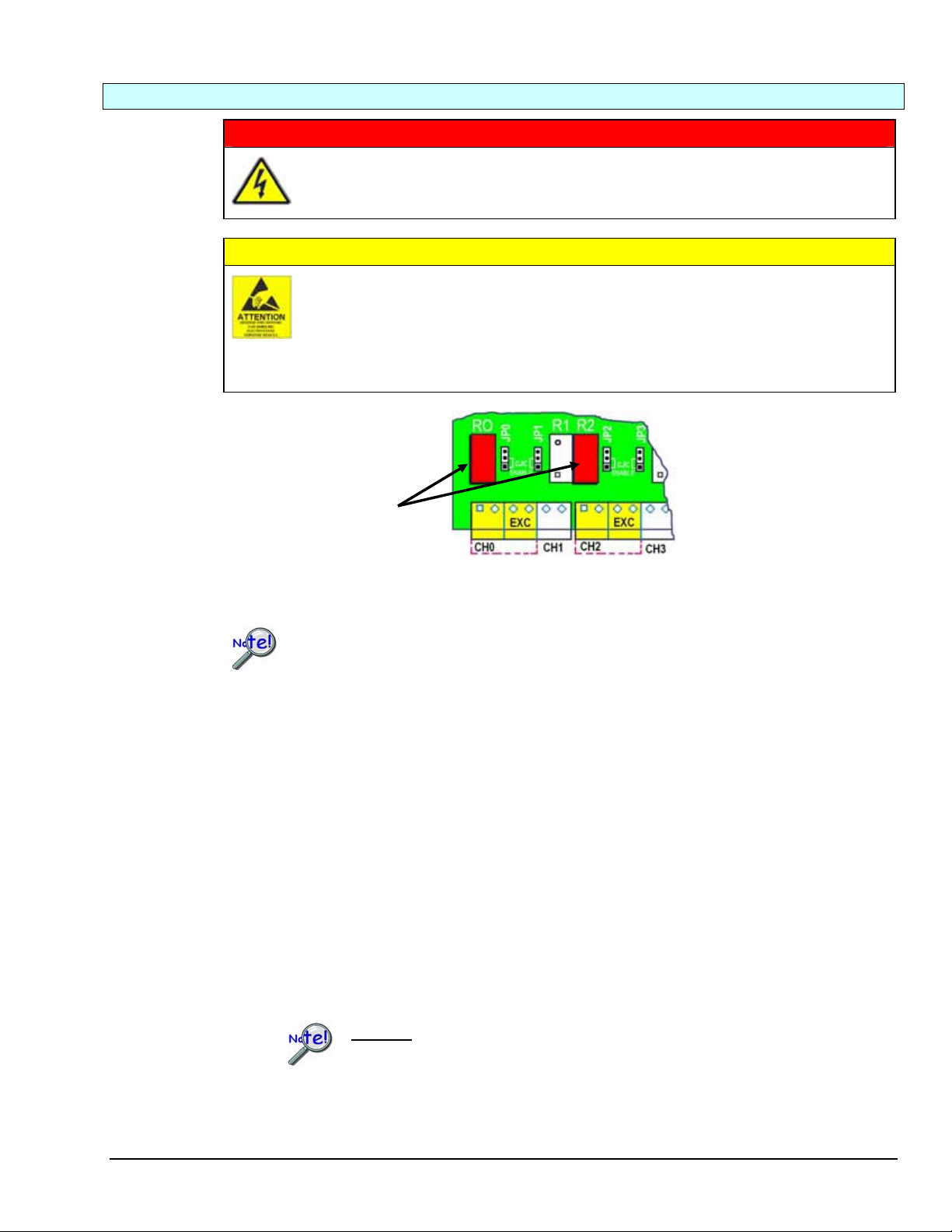
Installing Plug-in Resistors to Create 4 to 20 mA Loops
Electric shock hazard! Turn off power to the DBK48 and all connected modules and
devices before inserting or removing resistors. Failure to do so could lead to injury or
death due to electric shock.
CAUTION
The discharge of static electricity can damage some electronic components.
Semiconductor devices are especially susceptible to ESD damage. You should always
handle components carefully, and you should never touch connector pins or circuit
components unless you are following ESD guidelines in an appropriate ESD
controlled area. Such guidelines include the use of properly grounded mats and wrist
straps, ESD bags and cartons, and related procedures.
Current Shunt
Resistors
WARNING
Shown with resistors plugged-in for Channel 0 (at R0) and Channel 2 (at R2)
Location of Current Shunt Resistor Plug-In
Only current-input type modules require the plug-in resistors.
The plug-in resistors must be removed for all other module types.
Inputs to monitor the commonly used 4 to 20mA current loops most often employ a 250Ω precision
resistor to develop a 1 to 5 VDC voltage drop.
Ideally, a resistor for such purpose should have a 0.1% tolerance (or better) with a minimum power rating
of 0.25W and a temperature coefficient of at least 25ppm/°C.
Lower values of resistance, for example, 62.5Ω [for a lower voltage drop within the loop of 0.25 to 1.25
VDC] will require that the host data acquisition device use a gain o f x4 to maximize the signal resolution.
To create a 4 to 20mA current loop:
1. Turn off power to the DBK48 and all connected modules and devices.
2. Disconnect power, all equipment, and signal lines from the DBK48 prior to installing the
resistors. Be aware that isolated measurements can present lethal voltages!
3. Remove the DBK48 top cover plate and set aside.
4. Carefully plug the Current Shunt Resistor into the applicable plug-in location for the designated
channel; for example, R0 for Channel 0, R1 for Channel 1, R2 for Channel 2, etc. Repeat for
each channel as applicable.
DO NOT solder the Current Plug-In Resistors in place. Only current-input type
modules require these resistors. The plug-in resistors must be removed for all
other module types.
5. Reinstall the DBK48 top cover plate and secure in place.
8B Isolated Signal Conditioning Module 958893 DK48, pg. 5
Page 84
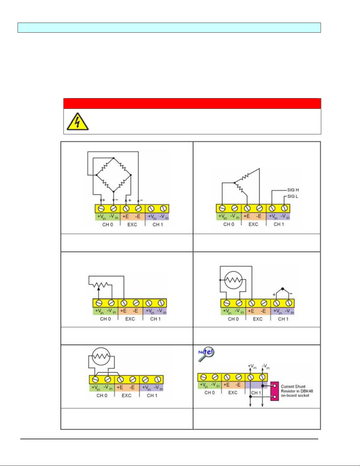
Making Terminal Block Connections
Input signals (and excitation when applicable) are wired to removable terminal blocks. Eight such blocks
can accept 2 channel inputs each. However, only channels 0, 2, 4, 6, 8, 10, 12, and 14 can be connected to
excitation. Thus the DBK48 is limited to 8 strain gages or 8 RTDs as only the even numbered channels
can be connected to excitation.
Each terminal block connects to a signal conditioning module within the DBK48. The blocks accept up to
14-gage wire into quick-connect screw terminals. Wiring schematics are provided below for RTDs,
thermocouples, 20 mA circuits, voltage (mV and V), and for full-bridge and half-bridge strain gages.
WARNING
Shock Hazard! The DBK48 is designed to sense signals that may carry dangerous
voltages. De-energize circuits connected to the DBK48 before changing the wiring or
configuration.
CH 0 is connected to a Full-Bridge Strain Gage.
CH 1 is shown not connected.
CH 0 is connected to a Half-Bridge Strain Gage.
CH 1 is connected for voltage input (mV or V).
CH 0 has a 3-wire connection to a potentiometer.
CH 1 is shown not connected.
CH 0 has a 3-wire connection to an RTD.
CH 1 is connected to a Thermocouple.
Only current-input type modules require the
plug-in resistors. The plug-in resistors must
be removed for all other module types.
CH 0 has a 2-wire connection to an RTD.
CH 1 is shown not connected.
CH 0 is shown not connected.
CH 1 is connected to a current shunt resistor
resulting in a 4 to 20 mA current loop.
DBK48, pg. 6 959893 8B Isolated Signal Conditioning Module
Page 85
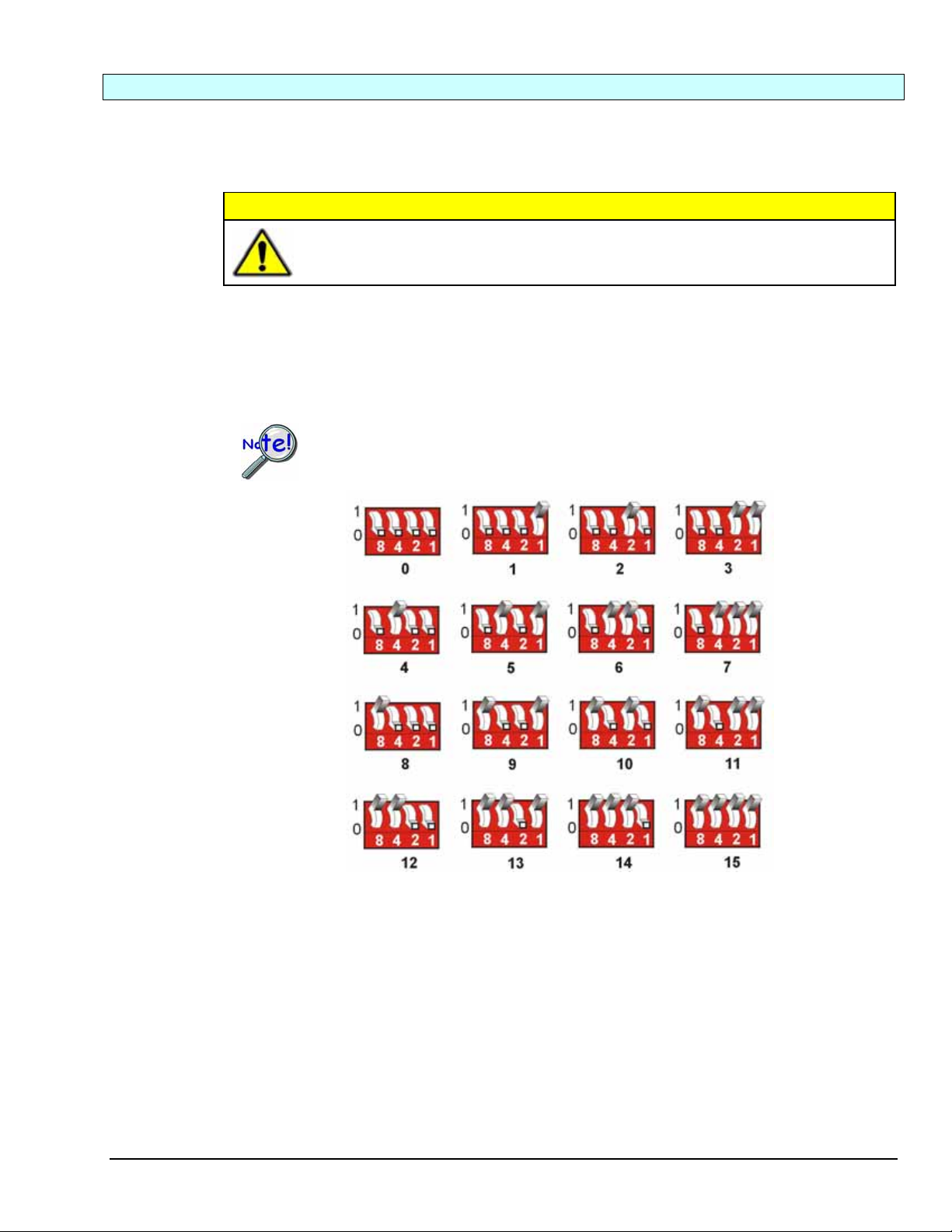
Setting DBK48 Module Addresses
Up to sixteen DBK48 modules can be attached to a single LogBook or Daq device. Each DBK48 module
must have a unique channel address because they connect to the primary data acquisition device via
parallel interface.
Adjustment of the channel address must only be performed when the system
power is OFF. Failure to do so may result in equipment damage.
To assign a channel address to the DBK48 module, first locate the DIP switch on the right side of the rear
panel. Four micro-switches [on the DIP switch] are used to set the module’s channel address in binary.
After ensuring that the system power is OFF, adjust the micro-switches to set the desired address. The 16
possible addresses are illustrated in the following figure.
Each module in the system must have a unique primary device channel address.
CAUTION
The 16 Possible Address Settings for DBK48 Modules
8B Isolated Signal Conditioning Module 958893 DK48, pg. 7
Page 86
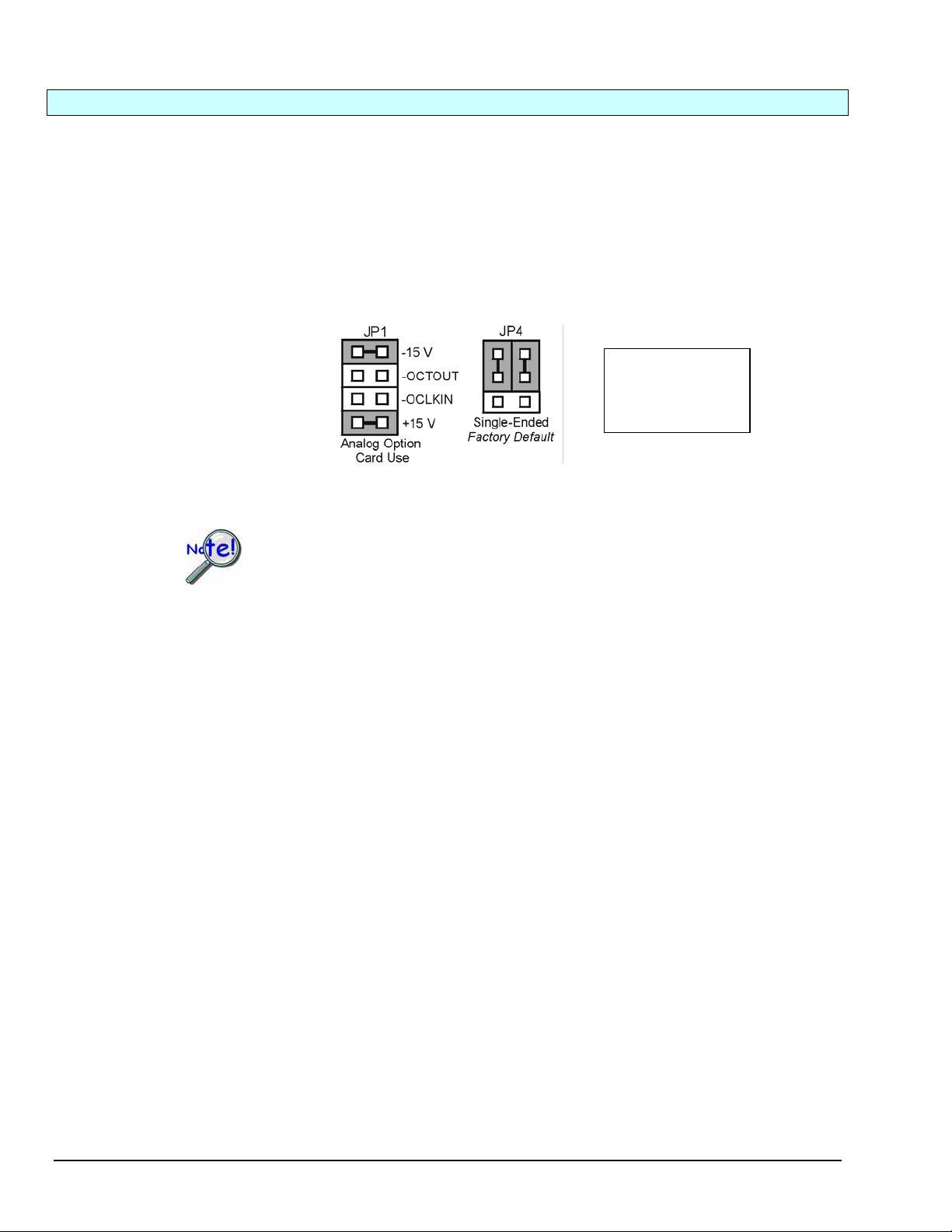
Configuring the Primary Data Acquisition Device
DaqBook/100 Series & /200 Series and DaqBoard [ISA type] Configuration
Use of a DBK48 with a DaqBook/100 Series, /200 Series devices, or with an ISA-type DaqBoard requires
the configuration of jumpers JP1 and JP4. These jumpers are located on the DaqBook/100 Series, /200
Series devices, and DaqBoard [ISA type] board.
1. If not using auxiliary power, set the JP1 jumper for Analog Option Card Use,
also referred to as the expanded analog mode.
Required Jumper Settings in DaqBook/100 Series & /200 Series and ISA-Type DaqBoards
Note:
These jumpers do not
apply to /2000 Series
Devices.
2. For DaqBook/100, DaqBook /112, and DaqBook /120 only, place the JP4 jumper in the single-ended
DaqBook/2000 Series, DaqBoard/2000 Series, DaqLab, and DaqScan
No jumper configurations are required on these Daq devices in regard to connecting a DBK48.
LogBooks
No jumper configurations are required on LogBook devices in regard to connecting a DBK48.
mode.
The JP1 default position (above) is necessary to power the interface circuitry of the
DBK48 via the internal ±15 VDC power supply. If using auxiliary power (e.g.,
DBK32A or DBK33) you must remove both JP1 jumpers.
For additional information refer to Power Requirements in the DBK Basics section and
to the DBK32A and DBK33 sections, as applicable.
DBK48, pg. 8 959893 8B Isolated Signal Conditioning Module
Page 87

CE Compliance
If your data acquisition system needs to comply with CE standards, the DBK48 must be connected to the
LogBook or Daq device by a CA-143-x cable. In addition, the CE compliant operating conditions must be
met as specified on the DBK48 module’s Declaration of Conformity card, which is shipped with the
module.
Reference Notes: If your data acquisition system needs to comply with CE standards,
refer to the following:
o the DBK48 Declaration of Conformity
o the CE Compliance section of Signal Management chapter of this manual
Connecting the DBK48 to the Primary Data Acquisition Device
Connect the DBK48 module as follows. Note that if your system needs to be CE Compliant, be sure to
read the preceding CE Compliance section prior to connecting the DBK48.
1. For a single DBK48 module, connect one end of the P1 cable to the module’s male DB37 output
connector.
For DaqBook applications - use a CA-37-x cable or a CA-255-xT cable.* •
•
For DaqBoard/2000 Series or /2000c Series boards - use a CA-37-x with a DBK200 Series
adapter.*
•
For DaqBoard [ISA type] boards - use a CA-131-x cable.*
* CA-37-x and CA-131-x cables do not meet CE compliance requirements. Refer to the
preceding CE section if CE compliance must be met.
2. Connect the free end of the cable to the P1 port of the LogBook or Daq device. For multiple DBK48
modules, use a CA-37-x (or CA-131-x) cable to daisy-chain several modules or an expansion
module. For example, three DBK48 modules could be connected to a LogBook or a Daq device via
a
CA-37-3 cable.
Note: For longer cable runs you can use a CA-113 cable to add 6 ft of length.
8B Isolated Signal Conditioning Module 958893 DK48, pg. 9
Page 88
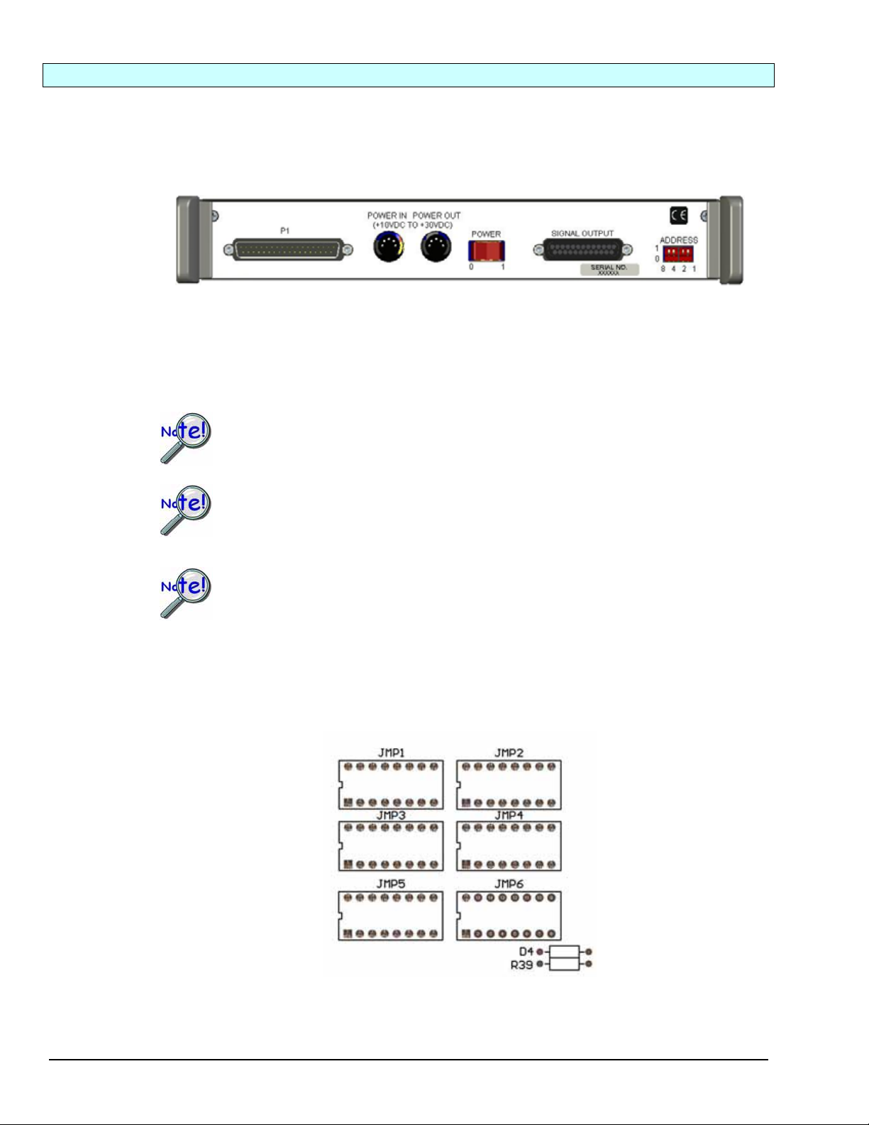
Using the DB25 Signal Output Connector
Important Notes Regarding the Signal Output Connector
The signal output connector on the rear panel of the DBK48 can be used to directly measure the output
voltage of each 8B module. This applies to input-type modules, i.e., volts, millivolts, thermocouple,
potentiometer, frequency, strain gage, RTD, etc.
DBK48 Rear Panel
The signal output connector can also be used with output-type 8B modules, e.g., current output and voltage
output. In this case a voltage is applied to the signal output connector. This voltage is converted to an
isolated current or isolated voltage by the 8B module which is installed in that channel. The isolated
current or voltage is available on the front panel terminal block.
Be careful when mixing 8B input modules and 8B output modules.
If possible, do not mix 8B input modules and 8B output modules within the same DBK48.
When applying voltages to the rear panel signal output connector [for 8B outputmodules] it can be easy to short to an adjacent pin on the 25 pin DSUB connector. If
there is an 8B input-module on that channel, damage may occur to that 8B module.
If a voltage source is being applied to a front panel terminal block for an 8B input-type
module and there is an 8B output-type module mistakenly installed in that channel,
damage to the 8B output module may occur.
Configuring the SIGNAL OUTPUT
The signal output connector on the rear panel of the DBK48 can be configured in one of two ways via
jumper networks that are placed in sockets JMP1, 2, 3, 4, 5, and 6.
Signal Output Configuration Jumpers
as Oriented on PCB
DBK48, pg. 10 959893 8B Isolated Signal Conditioning Module
Page 89
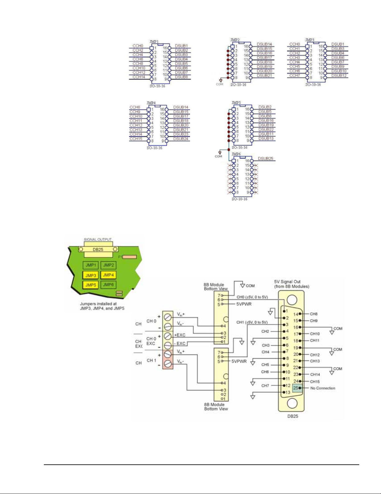
Jumper Assignments
JMP1 JMP2 JMP3
For JMP1 through JMP6:
CCHx = Single-ended I/O
JMP4
DSUBx = Pin x of the DB25
JMP5 and JMP6
Bringing all Sixteen 8B Module Outputs to the DB25 Signal Output Connector
With three CA-19-8 jumper networks installed [one per socket] in JMP3, JMP4,
and JMP5 the signal output connector is pinned out as shown in the following
figure. This brings the outputs of all sixteen 8B modules to the 25-pin DSUB
Signal Output connector on the rear panel.
channel of 8B
Module.
Signal Output
connector.
DB25 SIGNAL OUTPUT Pinout with JMP3, JMP4, JMP5 Installed
This configuration brings all 16 channel outputs to the DB25 Signal Output Connector.
8B Isolated Signal Conditioning Module 958893 DK48, pg. 11
Page 90
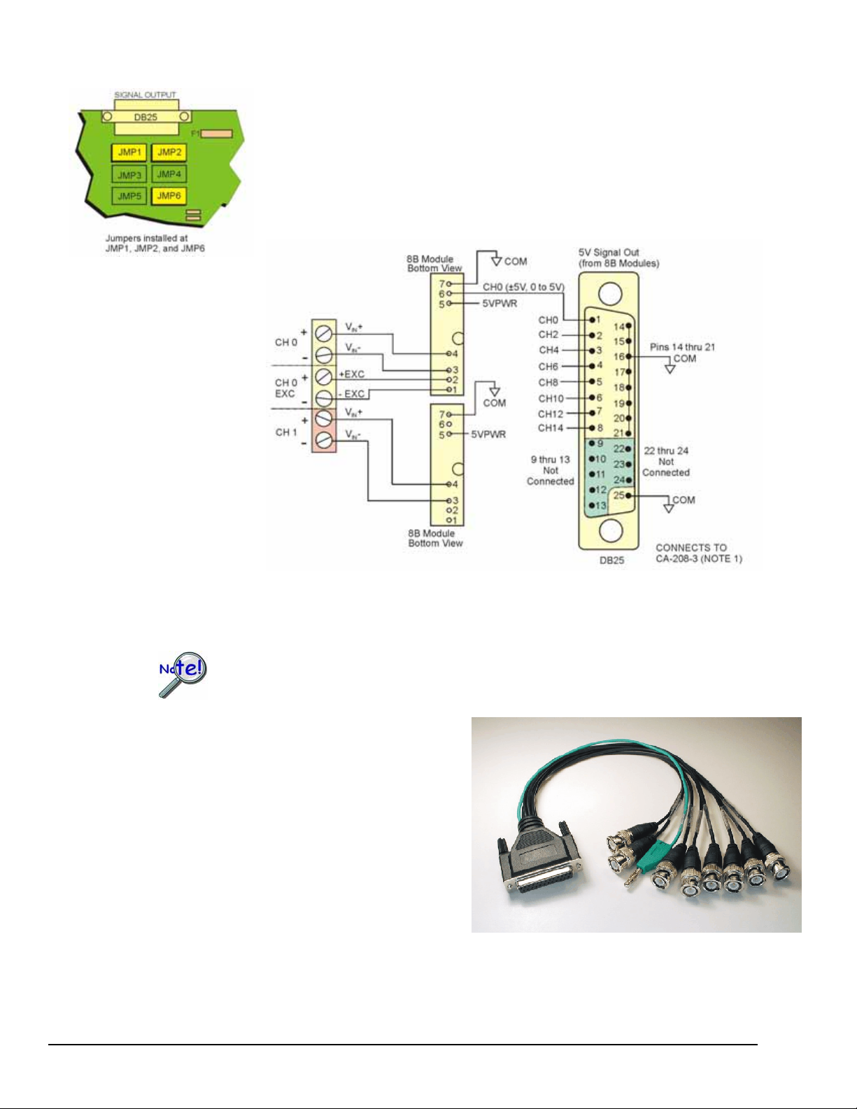
Bringing Eight 8B Module Outputs to the DB25 Signal Output Connector
With 3 jumper networks installed [one per socket] in JMP1, JMP2, and JMP6 the
signal output connector is pinned out as shown in the following figure. This only
brings the outputs of eight of the 8B modules, i.e., Ch 0, 2, 4, 6, 8, 10, 12, and 14.
When the Signal Output connector is pinned-out in this manner it can be used with a
CA-208-3 cable to bring the 8 channels out to the cable’s BNC connectors for easy
connection to other measuring equipment.
DB25 SIGNAL OUTPUT Pinout with JMP1, JMP2, JMP6 Installed
This configuration brings channel 0, 2, 4, 6, 8, 10, 12 and 14 outputs to the DB25
Signal Output Connector.
If the DBK48 is not connected to a Daq device via the P1 connector, then remove the Rnets
from S01 and S02. These resistor networks connect each 8B module’s output to the
multiplexer for P1.
Use the CA-208-3 cable as follows:
1. Connect the DB25-end of the CA-208-3 cable
directly to DBK48’s 25-pin Signal Output
connector.
2. Connect the CA-208-3 analog common banana
plug to the local ground of the measuring
equipment.
3. Connect the CA-208-3 BNC connectors (for
channels 1 through 8) to the measuring
equipment.
Note 1: CA-208-3 connects directly to the signal output connector. However, another cable, which looks virtually the
same, is the CA-208 (with no”-3” extension). If you are using a CA-208 you must first connect a CA-35-18
cable to the DB25 connector on the DBK48; then connect the CA-208 to the CA-35-18 cable. For CA-208
users, a wiring diagram is provided immediately following the DBK48 specifications section.
DBK48, pg. 12 959893 8B Isolated Signal Conditioning Module
Page 91
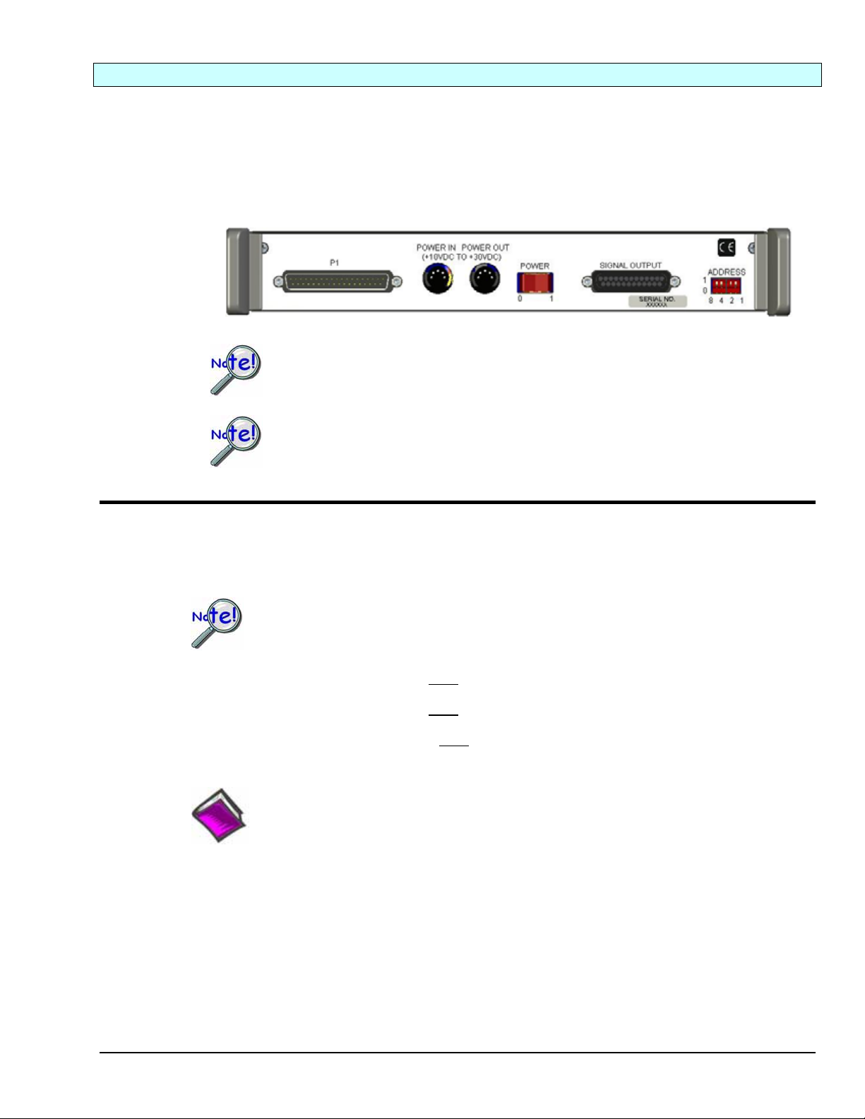
Powering the System
The DBK48 contains an internal power supply. The unit can be powered by an AC power adapter or any
10 to 30 VDC source, such as a 12 V car battery. For portable or field applications, DBK48 and the
primary Daq device can be powered by a DBK30A rechargeable battery module or DBK34 vehicle UPS
module. The supply input is fully isolated from the measurement system. If the fuse requires replacement,
use a
2 Amp Mini ATO Fuse, factory part number FU-8-2 (Littelfuse # 297-002).
Software Setup
You will need to set several parameters so DaqView can best meet your application requirements.
After the 8B module type is identified, DaqView figures out the m and b (of the mx+b equation) for proper
engineering units scaling. An example of the mx + b equation follows shortly.
DBK48 Rear Panel
DBK48’s internal power supply supplies power to the 8B modules only. The DIN5
Power Out connector is a pass-through to allow for a power daisy-chain.
Prior to daisy-chaining from one module’s power connector to another, be sure to
compute the power consumption for the entire system. Some modules may need
independent power adapters. See chapter 2 for information regarding power supply
issues.
LogView does not include the means to directly select the DBK48.
To use a DBK48 and
its 8B modules with LogBook: Select DBK42 in LogView. This will recognize the DBK48, but
will identify it as a DBK42. For each 8B module, select the 5B module that exhibits the same
measurement ranges; three examples follow:
For SC-8B30-01 select SC-5B30-01 as both have an Input Range of ±10 mV;
and an Output Range of ±5V.
For SC-8B34-02
with an Input Range of 0°C to +100°C.
For SC-8B47-T-07
with an Input Range of 0°C to +200°C.
select SC-5B34-02 as both are Type 100 Ohm Pt;
select SC-5B47-T-07 as both are a Type T Thermocouple,
Reference Note:
o For DaqView information refer to chapter 3, DBK Setup in DaqView and to the DaqView
PDF included on your data acquisition CD.
o For LogView information refer to chapter 4, DBK Setup in LogView and to the LogView
section of the LogBook PDF included on your data acquisition CD. Also, see above
note.
o The API includes functions applicable to the DBK48. Refer to related material in the
Programmer’s Manual (p/n 1008-0901) as needed.
PDF Note:
During software installation, Adobe
®
PDF versions of user manuals automatically install onto
your hard drive as a part of product support. The default location is in the Programs group,
which can be accessed from the Windows Desktop. Refer to the PDF documentation for
details regarding both hardware and software. Note that you can also access PDF documents
directly from the data acquisition CD via the <View PDFs> button on the CD’s opening
screen.
8B Isolated Signal Conditioning Module 958893 DK48, pg. 13
Page 92
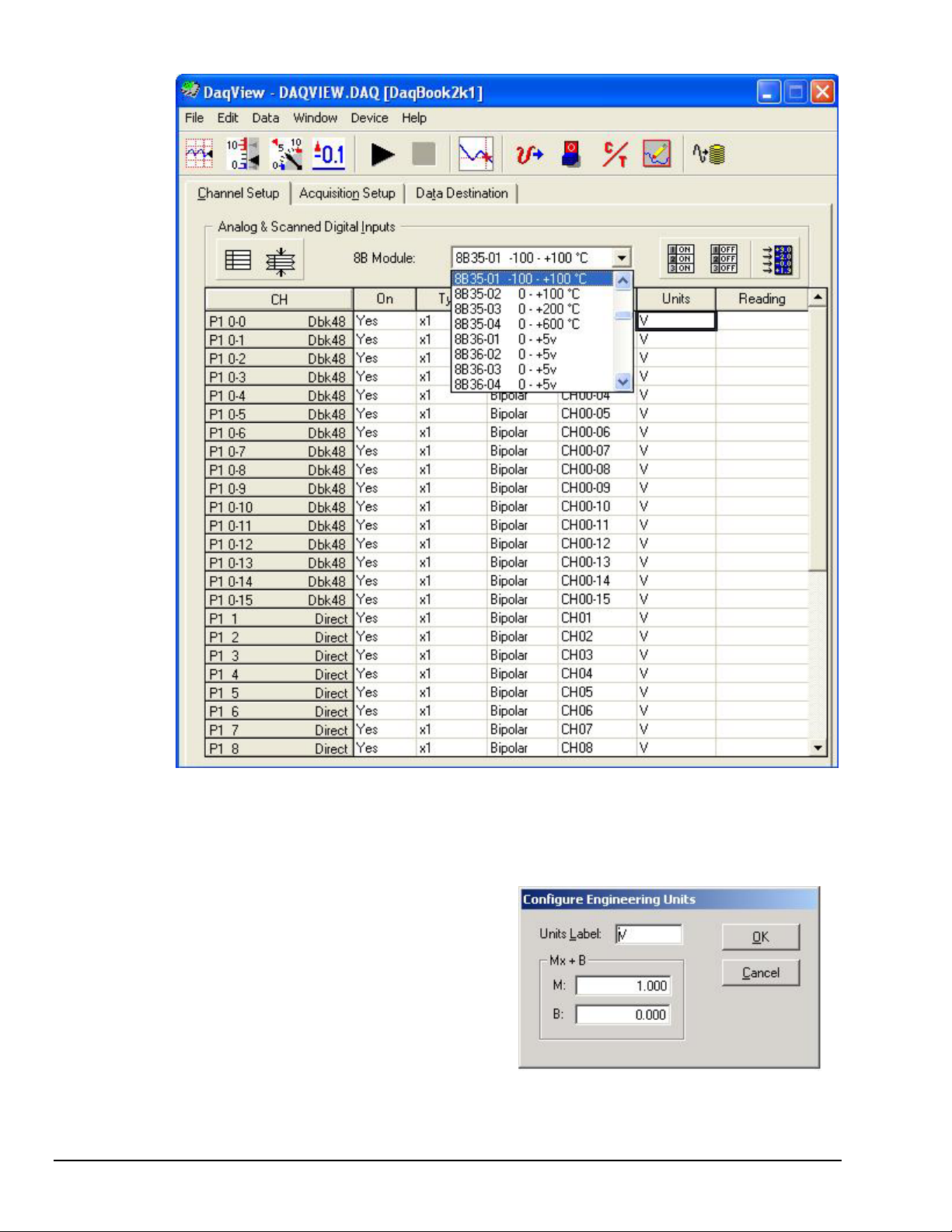
DaqView Configuration Main Window
mX +b, an Example
The Customize Engineering Units dialog box can be
accessed via the DaqView Configuration main
window by activating the Units cell [for the desired
channel], then clicking to select mX+b.
From the Customize Engineering Units dialog box
(see figure at right), you can enter values for m and b
components of the equation that will be applied to
the data. There is also an entry field that allows you
to enter a label for the new units that may result from
the mX+b calculation.
An example of mX + b equation use follows.
DBK48, pg. 14 959893 8B Isolated Signal Conditioning Module
Page 93

Engineering Units Conversion Using mx + b
Most of our data acquisition products allow the user to convert a raw signal input (for example, one that is
in volts) to a value that is in engineering units (for example, pressure in psi). The products accomplish this
by allowing the user to enter scale and offset numbers for each input channel, using the software associated
with the product. Then the software uses these numbers to convert the raw signals into engineering units
using the following “mx + b” equation:
(1) Engineering Units = m(Raw Signal) + b
The user must, however, determine the proper values of scale (m) and offset (b) for the application in
question. To do the calculation, the user needs to identify two known values: (1) the raw signal values, and
(2) the engineering units that correspond to the raw signal values. After this, the scale and offset
parameters can be calculated by solving two equations for the two unknowns. This method is made clear
by the following example.
Example
An engineer has a pressure transducer that produces a voltage output of 10.5 volts when the measured
pressure is 3200 psi. The same transducer produces an output of 0.5 volt when the pressure is 0 psi.
Knowing these facts, m and b are calculated as follows.
A - Write a pair of equations, representing the two known points:
(2) 3200 = m(10.5) + b
(3) 0 = m(0.5) + b
B - Solve for m by first subtracting each element in equation (3) from equation (2):
(4) 3200 - 0 = m(10.5 – 0.5) + (b - b)
(5)
Simplifying gives you: 3200 = m(10)
(6)
This means: m = 320
C - Substitute the value for m into equation (3) to determine the value for b:
(7) 0 = 320 (0.5) + b
(8)
Therefore: b = - 160
Now it is possible to rewrite the general equation (1) using the specific values for m and b that we just
determined:
(9) Engineering Units = 320(Raw Signal) - 160
The user can then enter the values of m and b into the appr opriate location using the facilities provided by
compatible data acquisition software, for example: WaveView, DaqView, Personal DaqView, LogView, and
TempView. The software uses equation (9) to calculate signal values in engineering units from that point
on.
8B Isolated Signal Conditioning Module 958893 DK48, pg. 15
Page 94

Specifications – DBK48
Name/Function: DBK48, 16-slot Multi-Purpose Isolated Signal Conditioning Module
Operating Environment:
Temperature: -30°C to 70°C
Relative Humidity: 95% RH, non-condensing
Connectors:
System Connector: DB37 male, mates with P1 connector on primary acquisition device (
Signal Connector: DB25, 5V output signals from the 8B modules
Power Connectors: Two DIN5 connectors; “Power In” and “Power Out” for daisy-chaining
Input Connections:
8 sets of removable screw terminal blocks, each with 6 connection points as follows:
1
1
2
Shunt-Resistor Socket: R0 through R15, plug-in resistor sockets.
Cold-Junction Sensor: Enabled or disabled per channel via jumpers JP0 through JP15.
8B Module Capacity:
o Up to 16 voltage input
o Up to 16 thermocouple
o Up to 8 modules which require excitation; i.e.
strain gauge, potentiometer, RTD
See latest catalog or contact your sales representative in regard to
the types of 8B Modules available for your application.
Power Requirements: 10 to 30 VDC; or 120 VAC with AC-to-DC adapter
With 16 thermocouple-type modules (0.03 amps each):
10 VDC @ 0.30 A
15 VDC @ 0.20 A
25 VDC @ 0.12 A
With 8 strain-gage-type modules (0.2 amps each):
10 VDC @ 1.000 A
15 VDC @ 0.667 A
25 VDC @ 0.400 A
Power Consumption: 750 mW from P1, typical
Channel-to-Channel Settling: ±0.05%, typical at 200kHz; ±0.025%, typical at 100kHz
DC Input Fuse: 2 Amp, Mini ATO Fuse, FU-8-2 (Littelfuse #297-002); at board location F3
Isolation
Input Power to System: 250 VDC
Signal Inputs to System: 250 VDC
Input Channel-to-Channel: 250 VDC
Dimensions: 285 mm W × 220 mm D × 45 mm H (11” x 8.5” × 1.75”)
Weight: 1.13 kg (2.5 lb) with no modules installed
st
channel voltage in (+V in, -V in)
st
channel excitation (+E, -E) (Note 2)
nd
channel voltage in (+V in, -V in)
One socket per channel for current loop inputs.
(±15V @ 25mA)
Note 1)
Note 1: If attachment to the primary device is through a 100-pin P4 connector, a DBK200 series adapter must be used to
Note 2: Input devices that require excitation can only be connected to the following channels:
DBK48, pg. 16 959893 8B Isolated Signal Conditioning Module
obtain the mating P1 connector.
0, 2, 4, 6, 8, 10, 12, 14. The odd-numbered channels do not connect to excitation.
Page 95
8B Module Ranges
Voltage Input Modules (3 Hz BW)
Part No. Input Range Output Range
SC-8B30-01 ±10 mV ±5V
SC-8B30-02 ±50 mV ±5V
SC-8B30-03 ±100 mV ±5V
SC-8B31-01 ±1 V ±5V
SC-8B31-02 ±5 V ±5V
SC-8B31-03 ±10 V ±5V
SC-8B31-04 ±1 V 0 to +5V
SC-8B31-05 ±5 V 0 to +5V
SC-8B31-06 ±10 V 0 to +5V
SC-8B31-07 ±20 V ±5V
SC-8B31-08 ±20 V 0 to +5V
SC-8B31-09 ±40 V ±5V
SC-8B31-10 ±40 V 0 to +5V
SC-8B31-12 ±60 V ±5V
SC-8B31-13 ±60 V 0 to +5V
Current Input Modules (3 Hz)
Part No. Input Range Output Range
SC-8B32-01 4 to 20 mA 0 to +5V
SC-8B32-02 0 to 20 mA 0 to +5V
Linearized 2-wire or 3-wire RTD Modules
(0 to +5V Output, 3 Hz BW) Type: 100Ω Pt RTD
[Available June 2005]
Part No. Input Range in ˚C ˚F
SC-8B34-01
SC-8B34-02 0 ˚C to +100˚C +32˚F to +212˚F
SC-8B34-03 0˚C to +200˚C +32˚F to +392˚F
SC-8B34-04 0 ˚C to +600˚C
-100˚C to +100˚C -148˚F to +212˚F
+32˚F to +1112˚F
Potentiometer Input Modules
(0 to +5V Output, 3 Hz BW)
[Available June 2005]
Part No. Input Range Output Range
SC-8B36-01 0 to 100Ω
SC-8B36-02 0 to 500Ω 0 to +5V
SC-8B36-03 0 to 1 kΩ 0 to +5V
SC-8B36-04 0 to 10 kΩ 0 to +5V
0 to +5V
Specifications are subject to change without notice.
8B Isolated Signal Conditioning Module 958893 DK48, pg. 17
Page 96
Voltage Input Modules (1 kHz BW)
Part No. Input Range Output Range
SC-8B40-01 ±10 mV ±5V
SC-8B40-02 ±50 mV ±5V
SC-8B40-03 ±100 mV ±5V
SC-8B41-01 ±1 V ±5V
SC-8B41-02 ±5 V ±5V
SC-8B41-03 ±10 V ±5V
SC-8B41-04 ±1 V 0 to +5V
SC-8B41-05 ±5 V 0 to +5V
SC-8B41-06 ±10 V 0 to +5V
SC-8B41-07 ±20 V ±5V
SC-8B41-08 ±20 V 0 to +5V
SC-8B41-09 ±40 V ±5V
SC-8B41-10 ±40 V 0 to +5V
SC-8B41-12 ±60 V ±5V
SC-8B41-13 ±60 V 0 to +5V
Linearized Thermocouple Input Modules
(0 to +5V Output, 3 Hz BW)
Part No. Type Input Range in ˚C ˚F
SC-8B47-J-01 J
SC-8B47-J-02 J -100˚C to +300˚C -148˚F to +572˚F
SC-8B47-J-03 J 0˚C to +500˚C +32˚F to +932˚F
SC-8B47-J-12 J -100˚C to +760˚C
SC-8B47-K-04 K 0˚C to +1000˚C
SC-8B47-K-05 K 0˚C to +500˚C
SC-8B47-K-13 K -100˚C to +1350˚C
SC-8B47-K-14 K 0˚C to +1200˚C
SC-8B47-T-06 T -100˚C to +400˚C
SC-8B47-T-07 T 0˚C to +200˚C
0˚C to +760˚C 32˚F to +1400˚F
-148˚F to +1400˚F
+32˚F to +1832˚F
+32˚F to +932˚F
-148˚F to +2462˚F
+32˚F to +2192˚F
-148˚F to +752˚F
+32˚F to +392˚F
Specifications are subject to change without notice.
DBK48, pg. 18 959893 8B Isolated Signal Conditioning Module
Page 97
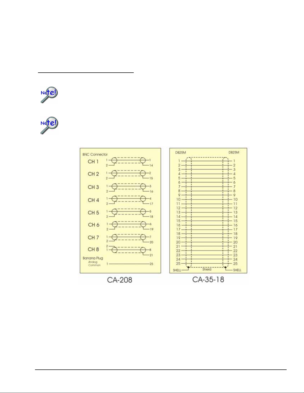
A NOTE FOR USERS OF CABLE CA-208
The following applies to customers using a CA-208 instead of a CA-208-3 cable.
Users of CA-208-3 are to ignore this material.
If the DBK48 is not connected to a Daq device via the P1 connector, then remove the Rnets from S01
and S02. These resistor networks connect each 8B module’s output to the multiplexer for P1.
DO NOT connect the CA-208 cable directly to the Signal Output connector. First connect a CA-35-18
cable to the DB25; then connect the CA-208 to the CA-35-18 cable. Both cables are required.
Wiring Diagrams
Use the two cables (CA-208 and CA-35-18) as follows:
1. Connect the CA-35-18 expansion cable to DBK48’s 25-pin Signal Output connector.
2. Connect DB25 end of the CA-208 cable to the CA-35-18 expansion cable.
3. Connect the CA-208 analog common banana plug to the local ground of the measuring equipment.
4. Connect the CA-208 BNC connectors (for channels 1 through 8) to the measuring equipment.
8B Isolated Signal Conditioning Module 958893 DK48, pg. 19
Page 98

This page is intentionally blank.
DBK48, pg. 20 959893 8B Isolated Signal Conditioning Module
Page 99
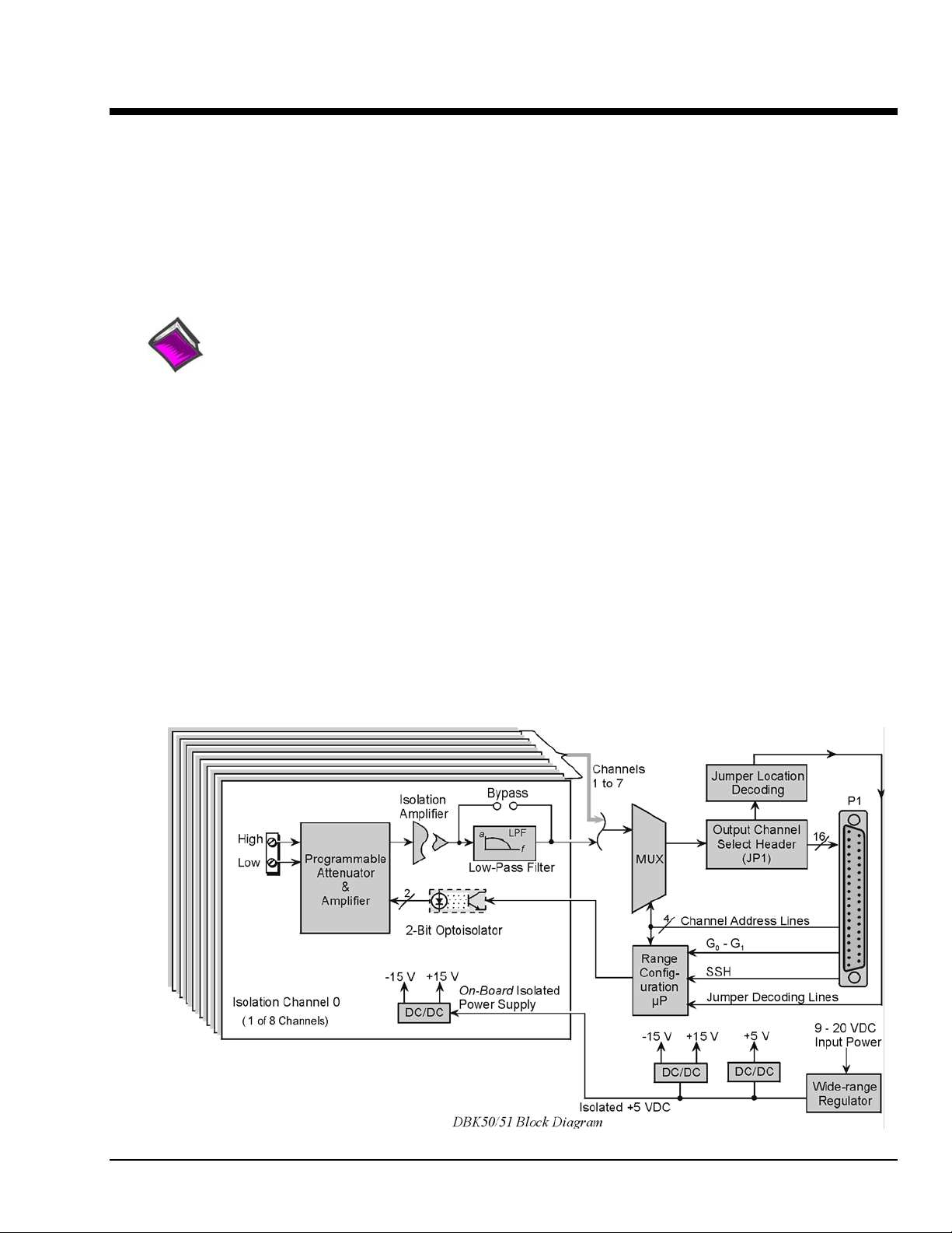
DBK50 and DBK51 8-Channel Isolated Voltage Input Modules
Overview …… 1
Input Attenuation/Gain Factors …… 2
Hardware Setup …… 2
Signal-to-Module Connection …… 2
Module Configuration …… 2
DaqBook/100 Series & /200 Series and DaqBoard [ISA type] Configuration …… 3
DaqBook/2000 Series and DaqBoard/2000 Series Configuration …… 4
Software Setup …… 4
DBK50 and DBK51 – Specifications …… 4
Reference Notes:
o Chapter 2 includes pinouts for P1, P2, P3, and P4. Refer to pinouts applicable to your
Overview
system, as needed.
o In regard to calculating system power requirements, refer to DBK Basics located near
the front of this manual.
Except for their ranges, the DBK50 (high-voltage) and the DBK51 (low-voltage) are identical. Both have
eight channels isolated from themselves (750 V) and from the LogBook or Daq Device analog common
(1250 V). Each channel’s input impedance is over 10 M
measured. Voltages can be read from DC to more than 20 kHz. One of three voltage ranges can be chosen
via software:
• for DBK50: ±10 V, ±100 V, or ±300 V.
• for DBK51: ±100 mV, ±1 V, or ±10 V.
Ω to minimize loading of the circuit being
With standard plug-in attenuator assemblies, the voltage ranges are interch angeable. The gain or
attenuation factor depends on the range, but the full-scale output for any range is +5 V.
Note: A fourth “range” delivers a shorted input voltage reading to allow offset compensation in some
applications.
DBK Option Cards and Modules 989594 DBK50 and DBK51, pg. 1
Page 100
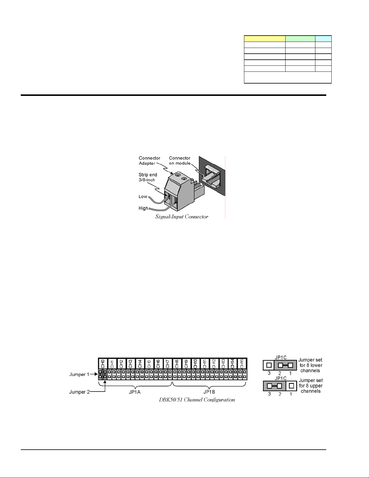
Input Attenuation/Gain Factors
Gain and attenuation may be calculated using the formula:
where: K is the attenuation or gain factor (the values of K for
available voltage ranges are given in the table).
Vin is the voltage applied to the module input channel.
Vout is the amplified or attenuated voltage from the module
output back to the main unit.
Hardware Setup
Signal-to-Module Connection
The DBK50/51 rear panel has 8 plug-in screw terminals for easy access to the 8 analog input channels.
There is a high (right side) and a low (left side) terminal in each pair to maintain consistent polarity (see
figure). For AC signals, the polarity is arbitrary unless multiple signals must maintain their phase
relationship.
K = Vin / Vout
Input Range Function K
300 V Range Attenuates 60
100 V Range Attenuates 20
10 V Range Attenuates 2
1 V Range Amplifies 0.2
100 mV Range Amplifies 0.02
Note: not all input ranges are
available on a single unit.
Module Configuration
Factory Default: Low-pass filter – Enabled
Several jumpers must be set on the DBK50 and DBK51 to match your application:
• 2 jumpers on JP1A or JP1B to select the main channel to use (see following figure).
• 1 jumper on JP1C for upper or lower sub channels
• 1 jumper on JPn02 to use or bypass the low-pass filter—one for each channel number (n)
The main output channel is one of the 16 primary data acquisition device [LogBook or Daq device]
channels. Each DBK50 [and DBK51] has 8 input channels and can be set to an upper or lower subchannel that allows 2 modules to share a single LogBook or Daq device channel. Thus, a fully-populated
system can have 256 input channels.
After determining a main channel number for the module, set two jumpers on JP1A or JP1B for the desired
channel. The two jumpers must be used side-by-side on the selected channel. This is illustrated for
channel 0 in the following figure. Next, set the JP1C jumper for the eight upper or eight lower subchannels. Note that two modules may share the same main channel if one is set to the upper sub channel
and the other set to the lower sub channel.
Each of the 8 input channels has a 3-pole low-pass filter that may be manually selected or bypassed by
positioning 2 shunt jumpers on 2×2 headers for each channel. Orient the jumpers parallel/horizontal
(enable) or perpendicular/vertical (bypass) to the header label (JP102 to JP802 for each of 8 channels).
The following figure can be used for orientation.
DBK50 and DBK51, pg. 2 989594 DBK Option Cards and Modules
 Loading...