

Page 1

Page 2

OMEGAnetSM On-Line Service
http://www.omega.com
Servicing North America:
Internet e-mail
info@omega.com
USA:
Canada:
One Omega Drive, Box 4047
Stamford, CT 06907-0047
Tel: (203) 359-1660
e-mail: info@omega.com
976 Berger
Laval (Quebec) H7L 5A1
Tel: (514) 856-6928
e-mail: canada@omega.com
FAX: (203) 359-7700
FAX: (514) 856-6886
For immediate technical or application assistance:
USA and Canada:
Mexico and
Latin America:
Sales Service: 1-800-826-6342 / 1-800-TC-OMEGA
Customer Service: 1-800-622-2378 / 1-800-622-BEST
Engineering Service: 1-800-872-9436 / 1-800-USA-WHEN
TELEX: 996404 EASYLINK: 62968934 CABLE: OMEGA
Tel: (95) 800-TC-OMEGA
En Espanol: (95) 203-359-7803
SM
FAX: (95) 203-359-7807
e-mail: espanol@omega.com
SM
SM
SM
Servicing Europe:
Benelux:
Czech Republic:
France:
Germany/Austria:
United Kingdom:
It is the policy of OMEGA to comply with all worldwide safety and EMC/EMI regulations that
apply. OMEGA is constantly pursuing certification of its products to the European New Approach
Directives. OMEGA will add the CE mark to every appropriate device upon certification.
The information contained in this document is believed to be correct but OMEGA Engineering, Inc. accepts
no liability for any errors it contains, and reserves the right to alter specifications without notice.
WARNING: These products are not designed for use in, and should not be used for, patient connected applications.
Postbus 8034, 1180 LA Amstelveen, The Netherlands
Tel: (31) 20 6418405
Toll Free in Benelux: 06 0993344
e-mail: nl@omega.com
ul. Rude armady 1868
733 01 Karvina-Hranice
Tel: 420 (69) 6311899
e-mail:czech@omega.com
9, rue Denis Papin, 78190 Trappes
Tel: (33) 130-621-400
Toll Free in France: 0800-4-06342
e-mail: france@omega.com
Daimlerstrasse 26, D-75392 Deckenpfronn, Germany
Tel: 49 (07056) 3017
Toll Free in Germany: 0130 11 21 66
e-mail: germany@omega.com
25 Swannington Road,
Broughton Astley, Leicestershire,
LE9 6TU, England
Tel: 44 (1455) 285520
FAX: 44 (1455) 283912
Toll Free in England: 0800-488-488
e-mail: uk@omega.com
FAX: (31) 20 6434643
FAX: 420 (69) 6311114
FAX: (33) 130-699-120
FAX: 49 (07056) 8540
P.O. Box 7, Omega Drive,
Irlam, Manchester,
M44 5EX, England
Tel: 44 (161) 777-6611
FAX: 44 (161) 777-6622
Page 3

TABLE OF CONTENTS
GENERAL DESCRIPTION .............................................................................................................. 2
OM5 SELECTION GUIDE ............................................................................................................... 2
ANALOG VOLTAGE INPUT MODULES, NARROW BANDWIDTH: OM5-IMV/IV ....................... 4
ANALOG CURRENT INPUT MODULES: OM5-II .......................................................................... 6
TRUE RMS INPUT MODULES: OM5-IAC ..................................................................................... 8
LINEARIZED 2- OR 3-WIRE RTD INPUT MODULES: OM5-IP/IC/IN ..............................................10
LINEARIZED 4-WIRE RTD INPUT MODULES: OM5-IP4/IC4/IN4.............................................. 12
POTENTIOMETER INPUT MODULES: OM5-PT ......................................................................... 14
THERMOCOUPLE INPUT MODULES: OM5-ITC ........................................................................ 16
STRAIN GAGE INPUT MODULES, WIDE BANDWIDTH: OM5-WBS ....................................... 16
ANALOG CURRENT OUTPUT MODULES: OM5-IVI ................................................................. 20
ANALOG VOLTAGE INPUT MODULES, WIDE BANDWIDTH: OM5-WMV/WV ....................... 22
2-WIRE TRANSMITTER INTERFACE MODULES: OM5-TX ............................................................ 24
GENERAL PURPOSE INPUT MODULES, DC EXCITATION: OM5-DT .................................... 26
FREQUENCY INPUT MODULES: OM5-IFI ................................................................................ 28
LINEARIZED THERMOCOUPLE INPUT MODULES: OM5-LTC ...................................................... 30
VOLTAGE OUTPUT MODULES, 50mA DRIVE CAPACITY: OM5-AV ...................................... 32
DIMENSIONS AND ACCESSORIES ............................................................................................ 34
1
Page 4
OM5-WMV/WV
Analog Voltage Input Modules, Wide Bandwidth
FEATURES
● ACCEPTS MILLIVOLT AND VOLTAGE LEVEL SIGNALS
● HIGH LEVEL VOLTAGE OUTPUTS
● 1500Vrms TRANSFORMER ISOLATION
●
ANSI/IEEE C37.90.1-1989
● INPUT PROTECTED TO 240VAC CONTINUOUS
● 100dB CMR
● 10kHz SIGNAL BANDWIDTH
● ±0.05% ACCURACY
● ±0.02% LINEARITY
● ±1µV/°C DRIFT
● CSA CERTIFIED, FM APPROVED, CE COMPLIANT
● MIX AND MATCH OM5 TYPES ON BACKPANEL
TRANSIENT PROTECTION
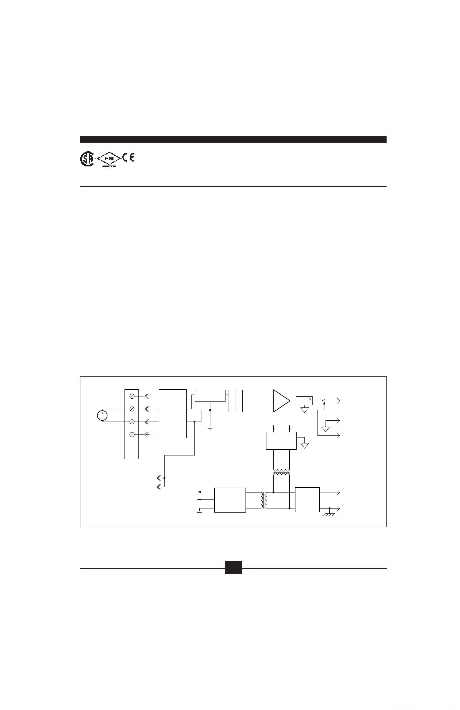
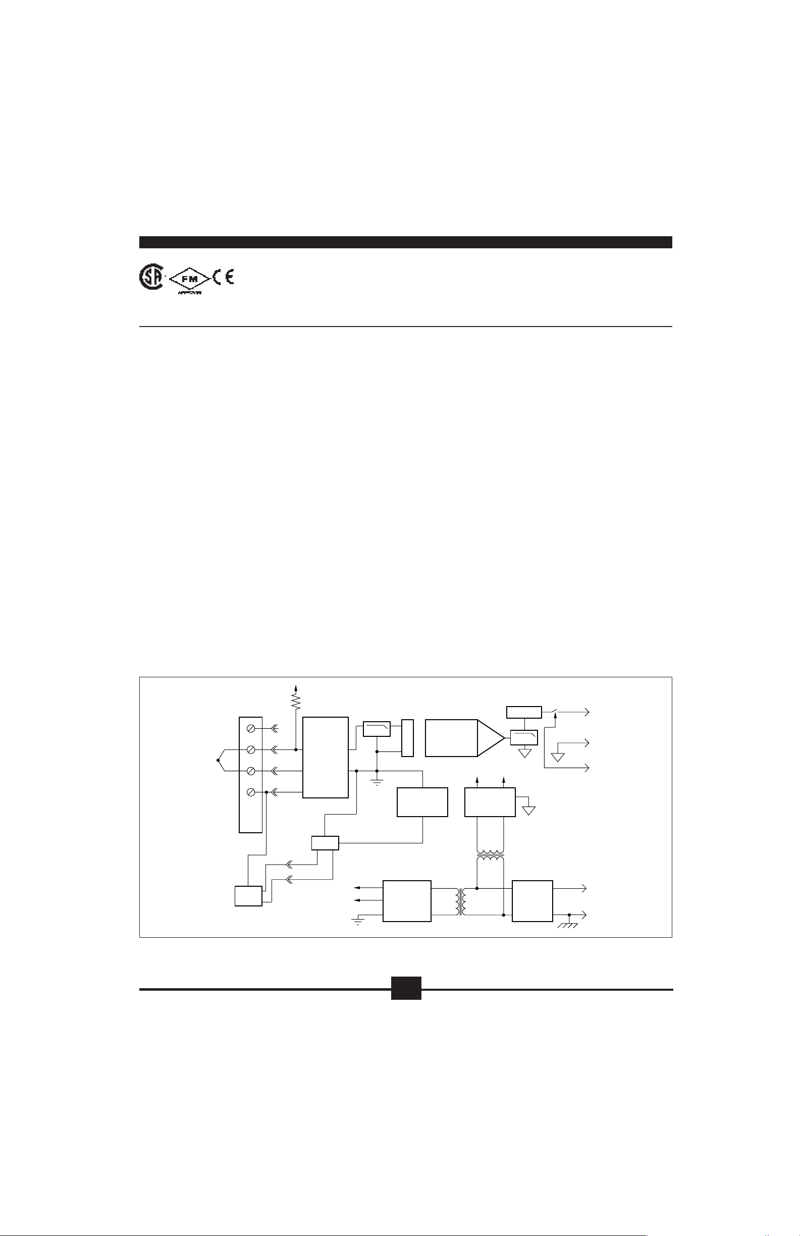
DESCRIPTION
Each OM5 wide bandwidth voltage input module provides a single channel
of analog input which is amplified, isolated, and converted to a high level
analog voltage output (Figure 1). This voltage output is logic-switch
controlled, allowing these modules to share a common analog bus without
the requirement of external multiplexers.
The OM5 modules are designed with a completely isolated computer side
circuit which can be floated to ±50V from Power Common, pin 16. This
complete isolation means that no connection is required between I/O
Common and Power Common for proper operation of the output switch. If
desired, the output switch can be turned on continuously by simply
connecting pin 22, the Read-Enable pin to I/O Common, pin 19.
The input signal is processed through a pre-amplifier on the field side of
the isolation barrier. This pre-amplifier has a gain-bandwidth product of
5MHz and is bandwidth limited to 10kHz. After amplification, the input
signal is chopped by a proprietary chopper circuit. Isolation is provided by
transformer coupling, again using a proprietary technique to suppress
transmission of common mode spikes or surges. The module is powered
from +5VDC, ±5%.
A special input circuit provides protection against accidental connection of
power-line voltages up to 240VAC.
4
6
5
3
NC
NC
Suppression
Protection
1
2
V
IN
+EXC
–EXC
+In
–In
Backpanel
Term Block
4
3
2
1
FIGURE 1. OM5-WMV/WV Block Diagram.
Surge
and
Anti-Aliasing
+V
–V
Filter
Isolated
Field-Side
Power
Isochopper™
Amplifier
Pat Pending
–V
+V
Isolated
Computer-Side
Power
LPF
Power
Oscillator
20
V
19
I/O Common
22
RD EN\
17
+5V
16
Power Common
OUT
22
Page 5

SPECIFICATIONS Typical at T
= +25°C and +5V Power.
A
Module OM5-WMV OM5-WV
Input Range ±10mV to ±100mV ±1V to ±40V
Input Bias Current ±0.5nA ±0.05nA
Input Resistance
Normal 200MΩ 650kΩ (minimum)
Power Off 40kΩ 650kΩ (minimum)
Overload 40kΩ 650kΩ (minimum)
Input Protection
Continuous 240Vrms Max *
Transient ANSI/IEEE C37.90.1-1989 *
CMV, Input to Output
Continuous 1500Vrms max *
Transient ANSI/IEEE C37.90.1-1989 *
CMR (50Hz or 60Hz) 100dB *
NMR (–3dB at 10kHz) 120dB per Decade above 10kHz *
(1)
Accuracy
±0.05% Span ±10µV RTI
Nonlinearity ±0.02% Span *
(2)
±0.05%(V
(3)
) ±0.05% span ±0.2mV RTI
Z
±0.05% (V
(3)
Z
(2)
)
Stability
Input Offset ±1µV/°C ±20µV/°C
Output Offset ±40µV/°C*
Gain ±25ppm/°C ±50ppm/°C
Noise
Input, 0.1 to 10Hz 0.4µVrms 2µVrms
Output, 100kHz 10mVp-p *
Bandwidth, –3dB 10kHz *
Rise Time, 10 to 90% Span 35µs*
Settling Time, to 0.1% 250µs*
Output Range ±5V or 0V to +5V *
Output Resistance 50Ω *
Output Protection Continuous Short to Ground *
Output Selection Time 6µs at C
(to ±1mV of V
Output Current Limit ±8mA *
)*
OUT
= 0 to 2000pF
load
Output Enable Control
Max Logic “0” +0.8V *
Min Logic “1” +2.4V *
Max Logic “1” +36V *
Input Current, “0”, “1” 0.5µA*
Power Supply Voltage +5VDC ±5% *
Power Supply Current 30mA *
Power Supply Sensitivity ±2µV/% RTI
(2)
±200µV/% RTI
(2)
Mechanical Dimensions 2.28" x 2.26" x 0.60" (58mm x 57mm x 15mm) *
Environmental
Operating Temp. Range –40°C to +85°C*
Storage Temp. Range –40°C to +85°C*
Relative Humidity 0 to 95% Noncondensing *
Emissions EN50081-1, ISM Group 1, *
Class A (Radiated, Conducted)
Immunity EN50082-1, ISM Group 1, Class A (ESD, RF, EFT) *
* Same specification as OM5WMV.
NOTES: (1) Includes nonlinearity,
hysteresis and repeatability.
(2) RTI = Referenced to input.
(3) VZ is the input voltage
that results in 0V output.
ORDERING
INFORMATION
MODEL INPUT RANGE OUTPUT RANGE
OM5-WMV-10A-C –10mV to +10mV –5V to +5V
OM5-WMV-50A-C –50mV to +50mV –5V to +5V
OM5-WMV-100A-C –100mV to +100mV –5V to +5V
OM5-WMV-10B-C –10mV to +10mV 0V to +5V
OM5-WMV-50B-C –50mV to +50mV 0V to +5V
OM5-WMV-100B-C –100mV to +100mV 0V to +5V
OM5-WV-1A-C –1V to +1V –5V to +5V
OM5-WV-5A-C –5V to +5V –5V to +5V
OM5-WV-10A-C –10V to +10V –5V to +5V
OM5-WV-1B-C –1V to +1V 0V to +5V
OM5-WV-5B-C –5V to +5V 0V to +5V
OM5-WV-10B-C –10V to +10V 0V to +5V
OM5-WV-20A-C –20V to +20V –5V to +5V
OM5-WV-20B-C –20V to +20V 0V to +5V
OM5-WV-40A-C –40V to +40V –5V to +5V
OM5-WV-40B-C –40V to +40V 0V to +5V
23
Page 6
OM5-TX
2-Wire Transmitter Interface Modules
FEATURES
● ISOLATED +20VDC CURRENT LOOP SUPPLY
● PROVIDES ISOLATION FOR NON-ISOLATED 2-WIRE
TRANSMITTERS
● HIGH LEVEL VOLTAGE OUTPUT: +1V to +5V or +2V to +10V
●
1500Vrms TRANSFORMER ISOLATION
● ANSI/IEEE C37.90.1-1989 TRANSIENT PROTECTION
● INPUT PROTECTED TO 240VAC CONTINUOUS
● 100dB CMR
● 100Hz SIGNAL BANDWIDTH
● ±0.05% ACCURACY
● ±0.02% LINEARITY
● CSA CERTIFIED, FM APPROVED, CE COMPLIANT
● MIX AND MATCH OM5 TYPES ON BACKPANEL
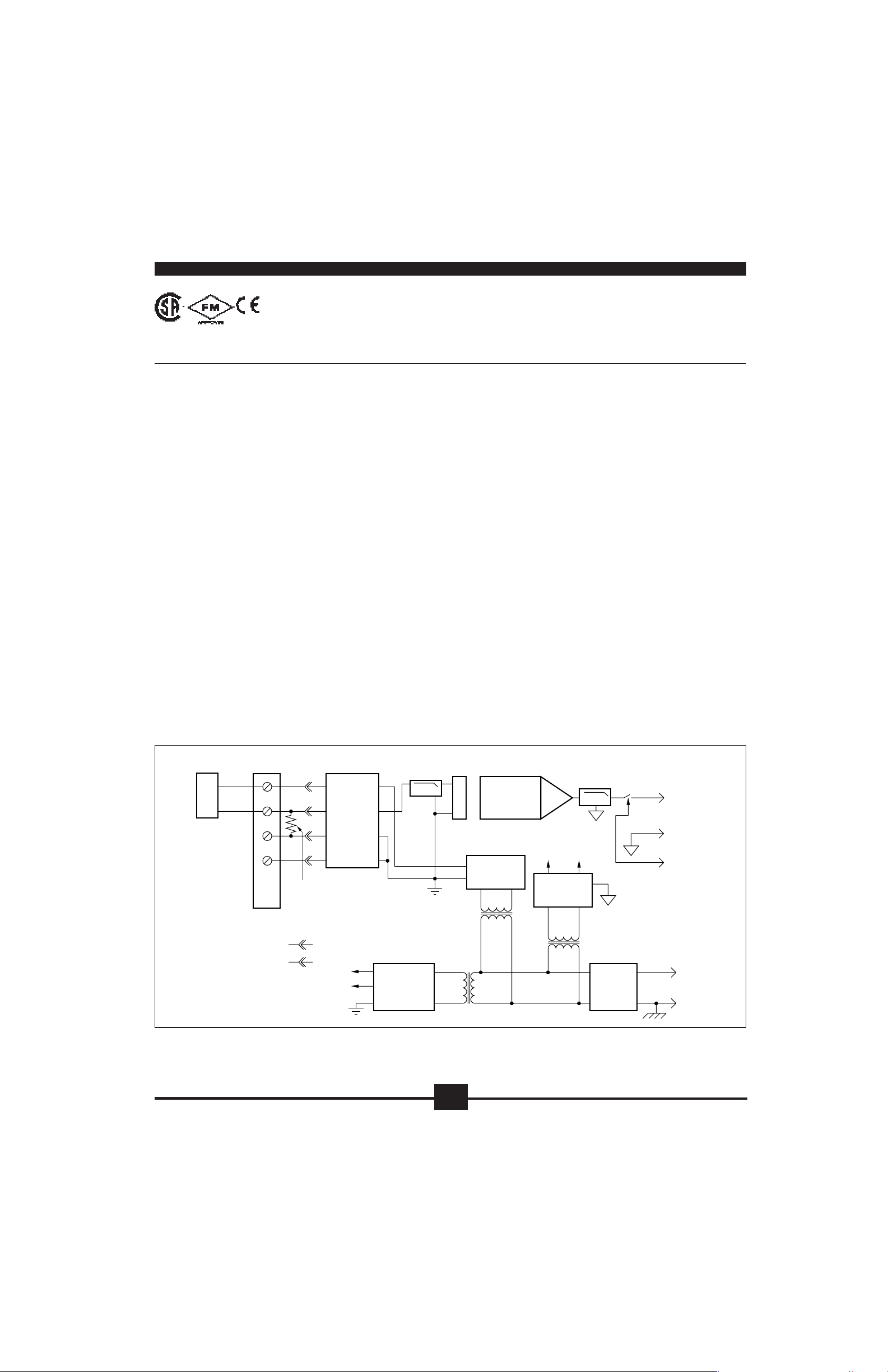
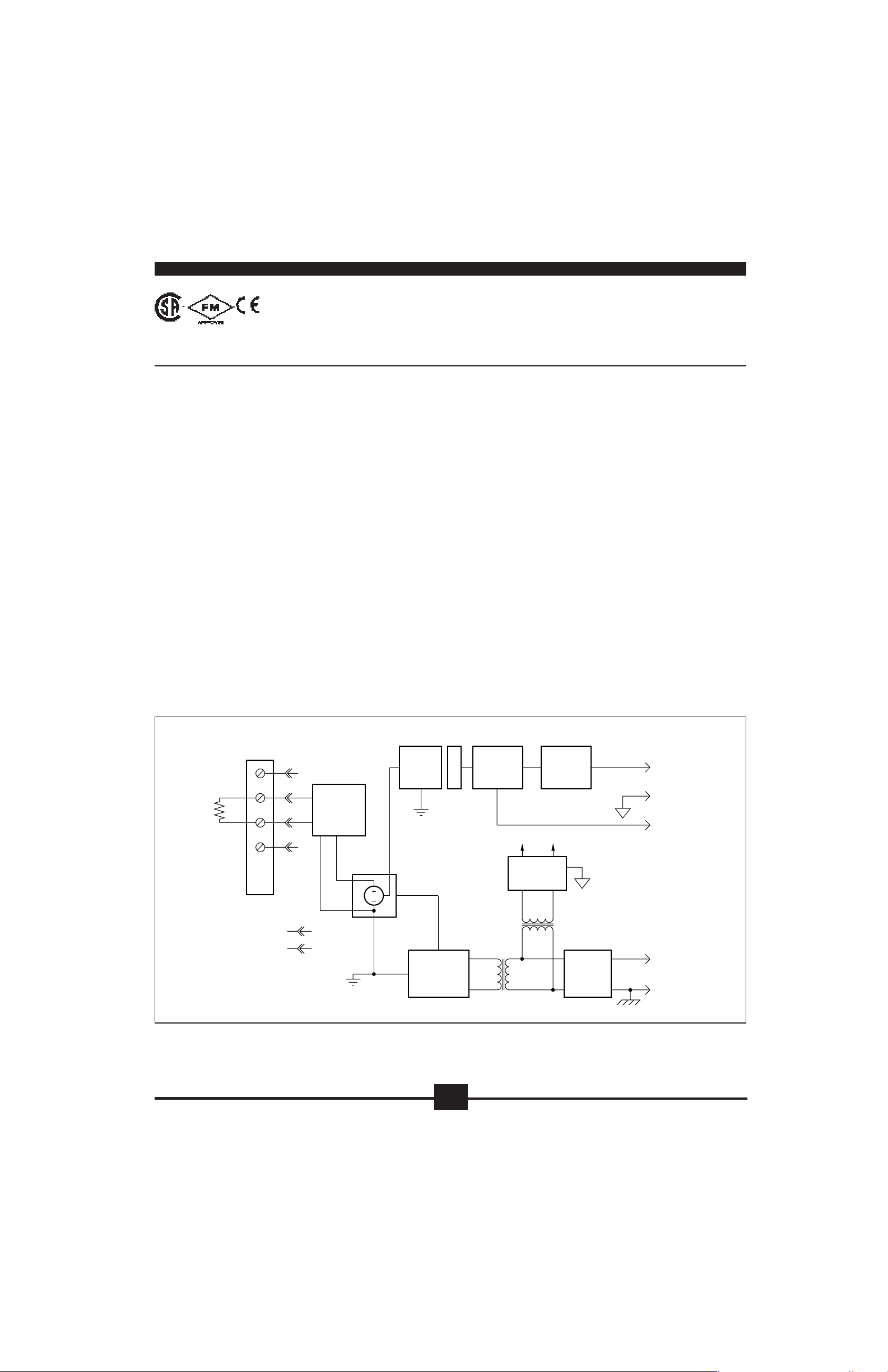
DESCRIPTION
Each OM5-TX 2-wire transmitter interface module provides a single channel which accepts a 4 to 20 mA process current input and provides a
standard +1 to +5V or +2 to +10V output signal (Figure 1). An isolated
+20VDC regulated power supply is provided to power the current transmit-
ter. This allows a 2-wire loop powered transmitter to be directly connected
to the module without requiring an external power supply. The regulated
supply will provide a nominal +20VDC at a loop current of 4mA to 20mA.
The OM5-TX will provide a 1500V isolation barrier for non-isolated 2-wire
field transmitters. It can also be used when additional isolation is required
between an isolated 2-wire transmitter and the input stage of the control
room computer.
The voltage output is logic switch controlled, which allows these modules
to share a common analog bus without the requirement of external
multiplexers.
The modules are designed with a completely isolated computer side circuit
which can be floated to ±50V from Power Common, pin 16. This complete
isolation means that no connection is required between I/O Common and
Power Common for proper operation of the output switch. If desired, the
output switch can be turned on continuously by simply connecting pin 22,
the Read-Enable pin to I/O Common, pin 19.
A precision 20Ω current conversion resistor is supplied with the module.
Sockets are provided on the OM5-BP backpanels to allow installation of
this resistor. Extra resistors are available under part number OMX-1362-C.
All field inputs are fully protected from accidental connection of power-line
voltages up to 240VAC. The module has a 3dB bandwidth of 100Hz. Signal
filtering is accomplished with a six-pole filter, with two poles on the field
side of the isolation barrier, and the other four on the computer side.
2-Wire
Transmitter
+EXC
4
+In
3
–In
2
–EXC
1
Backpanel
Term Block
0.1% plug-in
OMX-1362-C
FIGURE 1. OM5-TX Block Diagram.
20Ω
4
6
5
3
1
NC
2
NC
Surge
Suppression
and
Protection
+V
–V
Isolated
Field-Side
Power
LPF
Isochopper™
Amplifier
Pat Pending
Isolated
Excitation
Source
–V+V
Isolated
Computer-Side
Power
LPF
Power
Oscillator
20
19
22
V
OUT
I/O Common
RD EN\
17
+5V
16
Power
Common
24
Page 7

SPECIFICATIONS Typical at T
Module OM5-TX
Input Range 4mA to 20mA
Input Resistor
Value 20.00Ω
Accuracy ±0.1%
Stability ±10ppm/°C
Loop Supply Voltage Nominal 20V at 4mA to 20mA
Isolated Excitation Protection
Continuous 240Vrms max
Transient ANSI/IEEE C37.90.1-1989
Input Protection
Continuous 240Vrms max
Transient ANSI/IEEE C37.90.1-1989
CMV, Input to Output
Continuous 1500Vrms max
Transient ANSI/IEEE C37.90.1-1989
CMR (50 or 60Hz) 100dB
NMR (–3dB at 100Hz) 120dB per decade above 100Hz
(1)
Accuracy
Nonlinearity ±0.02% span
Stability
Input Offset ±1µV/°C
Output Offset ±40µV/°C
Gain ±25ppm/°C of reading
Noise
Input, 0.1 to 10Hz 10nArms
Output, 100KHz 500µVrms
Bandwidth, –3dB 100Hz
Response Time, 90% span 4mS
Output Range +1V to +5V or +2V to +10V
Output Resistance 50Ω
Output Protection Continuous short to gnd
Output Selection Time 6µs at C
(to ±1mV of V
Output Current Limit +8mA
Output Enable Control
Max Logic “0” +0.8V
Min Logic “1” +2.4V
Max Logic “1” +36V
Input Current, “0, 1” 0.5µA
Power Supply Voltage +5VDC ±5%
Power Supply Current 180mA at transmitter load of 20mA
Power Supply Sensitivity ±10µV/% RTI
Mechanical Dimensions 2.28" x 2.26" x 0.60" (58mm x 57mm x 15mm)
Environmental
Operating Temp. Range –40°C to +85°C
Storage Temp. Range –40°C to +85°C
Relative Humidity 0 to 95% noncondensing
Emissions EN50081-1, ISM Group 1, Class A (Radiated, Conducted)
Immunity EN50082-1, ISM Group 1, Class A (ESD, RF, EFT)
)
OUT
= +25°C and +5V power.
A
±0.05% span ±4µA RTI
= 0 to 2000pF
load
100mA at transmitter load of 4mA
(2)
(2)
SCM5B
NOTES: (1) Includes nonlinearity, hysteresis and repeatability.
(2) RTI = Referenced to input.
ORDERING INFORMATION
MODEL INPUT RANGE OUTPUT RANGE
OM5-TX-1-C 4mA to 20mA +1V to +5V
OM5-TX-2-C 4mA to 20mA +2V to +10V
25
Page 8
OM5-DT
General Purpose Input Modules, with DC Excitation
FEATURES
● INTERFACES TO DC DISPLACEMENT TRANSDUCERS AND OTHER
DEVICES REQUIRING A STABLE DC SUPPLY
● HIGH LEVEL VOLTAGE OUTPUTS
●
1500Vrms TRANSFORMER ISOLATION
● ANSI/IEEE C37.90.1-1989 TRANSIENT PROTECTION
● INPUT PROTECTED TO 240VAC CONTINUOUS
● FULLY ISOLATED EXCITATION SUPPLY
● 100dB CMR
● 1KHz SIGNAL BANDWIDTH
● ±0.10% ACCURACY
● ±0.02% LINEARITY
● ±20µV/°C DRIFT
● CSA CERTIFIED, FM APPROVED, CE COMPLIANT
● MIX AND MATCH OM5 TYPES ON BACKPANEL
DESCRIPTION
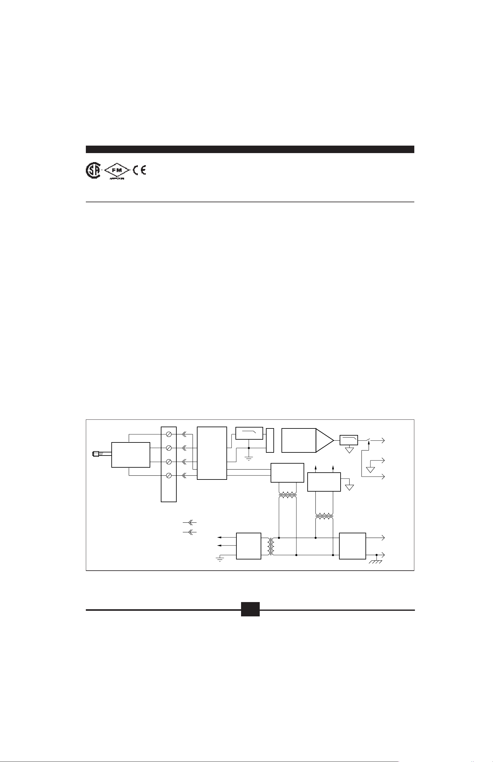
Each OM5-DT general purpose input module provides a single channel of
transducer input which is filtered, isolated, scaled, and converted to a high
level analog voltage output (Figure 1). This voltage output is logic switch
controlled, which allows these modules to share a common analog bus
without the requirement of external multiplexers.
The modules are designed with a completely isolated computer side circuit
which can be floated to ±50V from Power Common, pin 16. This complete
isolation means that no connection is required between I/O Common and
Power Common for proper operation of the output switch. If desired, the
output switch can be turned on continuously by simply connecting pin 22,
the Read-Enable pin to I/O Common, pin 19.
The OM5-DT can interface to devices which require a precision 10VDC
excitation supply. The 1kHz bandwidth significantly reduces ripple and
noise inherent in these devices.
Transducer excitation is provided from the module by a very stable 10V
source. The excitation supply is fully isolated, allowing the amplifier inputs
to operate over the full range of the excitation voltage. This feature offers
significant flexibility in real world applications. Eight full scale input ranges
are provided, from ±1V to ±10V, producing ±5V full scale output.
The input signal is processed through a pre-amplifier on the field side of
the isolation barrier. This pre-amplifier has a gain-bandwidth product of
5MHz and is bandwidth limited to 1kHz. After amplification, the input signal
is chopped by a proprietary chopper circuit. Isolation is provided by
transformer coupling, again using a proprietary technique to suppress
transmission of common mode spikes or surges. The module is powered
from +5VDC, ±5%.
Special input circuits provide protection of the signal inputs and the
isolated excitation supply up to 240VAC.
+EXC
DC LVDT
or Other
Transducer
+In
–In
–EXC
Backpanel
Term Block
FIGURE 1. OM5-DT Block Diagram.
4
4
3
2
1
6
5
3
2
Surge
Suppression
and
Protection
1
NC
NC
+V
–V
LPF
Isolated
Field-Side
Power
Isochopper™
Amplifier
Pat Pending
Isolated
Excitation
Source
+V
–V
Isolated
Computer-Side
Power
LPF
Power
Oscillator
20
19
22
17
16
V
OUT
I/O Common
RD EN\
+5V
Power
Common
26
Page 9

SPECIFICATIONS Typical at T
Module OM5-DT
Input Range ±1V to ±10V
Input Bias Current ±0.05nA
Input Resistance
Normal 2MΩ (minimum)
Power Off 2MΩ (minimum)
Overload 2MΩ (minimum)
Input Protection
Continuous 240Vrms max
Transient ANSI/IEEE C37.90.1-1989 (formerly IEEE-472)
Excitation Voltage, V
Excitation current 40mA (maximum)
Excitation Load Regulation ±5ppm/mA
Excitation Stability ±15ppm/°C
Isolated Excitation Protection
Continuous 240Vrms max
Transient ANSI/IEEE C37.90.1-1989 (formerly IEEE-472)
CMV, Input to Output
Continuous 1500Vrms max
Transient ANSI/IEEE C37.90.1-1989 (formerly IEEE-472)
CMR (50 or 60Hz) 100dB
NMR (–3dB at 1kHz) 120dB per decade above 1kHz
(1)
Accuracy
Nonlinearity ±0.02% span
Stability
Input Offset ±20µV/°C
Output Offset ±40µV/°C
Gain ±50ppm/°C
Noise
Input, 0.1 to 10Hz 0.4µVrms
Output, 100KHz 5mVpp
Bandwidth, –3dB 1kHz
Response Time (to 90% final value) 750µs
Output Range ±5V
Output Resistance 50Ω
Output Protection Continuous short to ground
Output Selection Time 6.0µs at C
(to ±1mV of V
Output Current Limit ±8mA
Output Enable Control
Max Logic “0” +0.8V
Min Logic “1” +2.4V
Max Logic “1” +36V
Input Current, “0, 1” 0.5µA
Power Supply Voltage +5VDC ±5%
Power Supply Current 200mA @ Full Exc. load, 100mA @ No Exc. Load
Power Supply Sensitivity ±200µV/% RTI
Mechanical Dimensions 2.28" x 2.26" x 0.60" (58mm x 57mm x 15mm)
Environmental
Operating Temp. Range –40°C to +85°C
Storage Temp. Range –40°C to +85°C
Relative Humidity 0 to 95% noncondensing
Emissions EN50081-1, ISM Group 1, Class A (Radiated, Conducted)
Immunity EN50082-1, ISM Group 1, Class A (ESD, RF, EFT)
NOTES:
(1) Includes excitation error, nonlinearity, hysteresis and repeatability.
(2) RTI = Referenced to input.
EXC
)
OUT
= +25°C and +5V power.
A
+10.0VDC ±2mV
±0.1% span, ±0.2mV RTI
= 0 to 2000pF
load
2
(2)
SCM5B
ORDERING INFORMATION
MODEL MAX IMU M INPUT OUTPUT
OM5-DT-1-C ±1V ±5V
OM5-DT-2-C ±2V ±5V
OM5-DT-3-C ±3V ±5V
OM5-DT-4-C ±4V ±5V
OM5-DT-5-C ±5V ±5V
OM5-DT-6-C ±6V ±5V
OM5-DT-7-C ±7V ±5V
OM5-DT-8-C ±8V ±5V
OM5-DT-9-C ±9V ±5V
OM5-DT-10-C ±10V ±5V
27
Page 10
OM5-IFI
Frequency Input Modules
FEATURES
● ACCEPTS FREQUENCY INPUTS OF 0 to 100kHz
● PROVIDES HIGH LEVEL VOLTAGE OUTPUTS
● TTL LEVEL INPUTS
● 1500 VOLT TRANSFORMER ISOLATION
● ANSI/IEEE C37.90.1-1989 TRANSIENT PROTECTION
● INPUT PROTECTED TO 240VAC CONTINUOUS
● ±0.05% ACCURACY
● MIX AND MATCH OM5 TYPES ON BACKPANEL
● CSA CERTIFIED, FM APPROVED, CE COMPLIANT
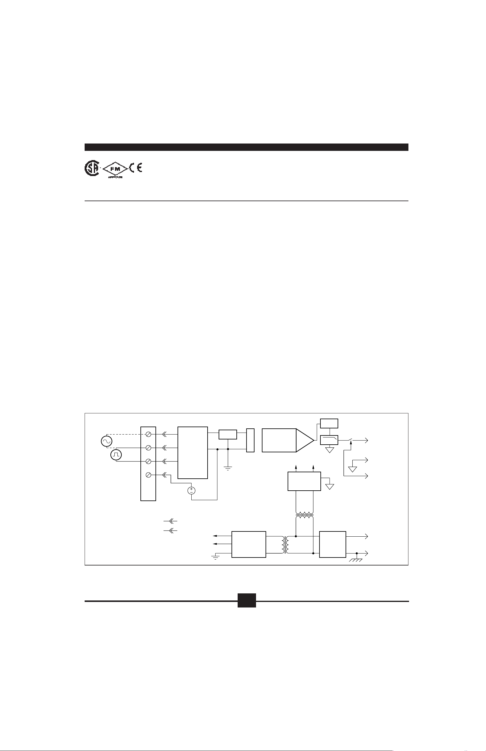
DESCRIPTION
Each OM5-IFI Frequency input module provides a single channel of frequency input which is isolated and converted to a high level analog voltage
output. This voltage output is logic switch controlled, which allows these
modules to share a common analog bus without the requirement of external
multiplexers (Figure 1).
The frequency input signal can be a TTL level signal or a zero-crossing signal.
Terminal 3 (+In) on the field-side terminal block is the “common” or ground
connection for input signals. A TTL signal is connected from terminal 2 (–In)
to terminal 3 (+In), while a zero-crossing signal is connected from terminal 4
(+EXC) to terminal 3 (+In). Input circuitry for each of the signal types has
hysteresis built in. An input signal must cross entirely through the hysteresis
region in order to trigger the threshold comparator.
A 5.1V excitation is available for use with magnetic pick-up or contactclosure type sensors. The excitation is available on pin 1 (–EXC) and the
excitation common is pin 3 (+In).
The modules are designed with a completely isolated computer side circuit
which can be floated to ±50V from Power Common, pin 16. This complete
isolation means that no connection is required between I/O Common and
Power Common for proper operation of the output switch. If desired, the
output switch can be turned on continuously by simply connecting pin 22,
the Read-Enable pin to I/O Common, pin 19.
A special circuit in the input stage of the module provides protection against
accidental connection of power-line voltages up to 240VAC.
Zero-Crossing
Inputs
+
–
–
+
+EXC
TTL
Inputs
–EXC
+In
–In
Backpanel
Term Block
4
3
2
1
FIGURE 1. OM5-IFI Block Diagram.
4
6
5
3
Surge
Suppression
and
Protection
1
NC
2
NC
5.1V
+V
–V
Threshold
Comparator
Isolated
Field-Side
Power
Signal
Isolation
–V
+V
Isolated
Computer-Side
Power
F to V
LPF
Power
Oscillator
20
V
19
I/O Common
22
RD EN\
17
+5V
16
Power Common
OUT
28
Page 11

SPECIFICATIONS Typical at Ta = +25C and +5V Power
Module OM5-IFI
Input Range 0 to 100KHz
Input Threshold Zero Crossing
Minimum Input 60mVp-p
Maximum Input 350Vp-p
Minimum Pulse Width 4µs
TTL Input Low 0.8V max
TTL Input High 2.4V min
Input Hysteresis
Zero Crossing 0.04V
TTL 1.5V
Input Resistance
Normal 100KΩ
Power Off 100KΩ
Overload 100KΩ
Input Protection
Continuous 240Vrms max
Transient ANSI/IEEE C37.90.1-1989
Excitation +5.1V @ 8mA max
CMV, Input to Output
Continuous 1500Vrms max
Transient ANSI/IEEE C37.90.1-1989
CMR (50 or 60Hz) 120dB
(1)
Accuracy
Nonlinearity ±0.02% span
Stability
Offset ±40ppm/°C
Gain ±40ppm/°C
Noise
Output Ripple <10mVp-p @ Input >2% span
Response Time (0 to 90%)
OM5-IFI-500/1K-C 300 ms
OM5-IFI-3K-C 170 ms
OM5-IFI-5K/10K-C 90 ms
OM5-IFI-25K/50K/100K-C 20 ms
Output Range 0V to +5V
Output Resistance 50Ω
Output Protection Continuous short to ground
Output Selection Time 6µs at C
(to ±1mV of V
Output Current Limit +8mA
Output Enable Control
Max Logic “0” +0.8V
Min Logic “1” +2.4V
Max Logic “1” +36V
Input Current, “0,1” 0.5µA
Power Supply Voltage +5VDC ±5%
Power Supply Current 110mA
Power Supply Sensitivity ±150µV/% RTO
Mechanical Dimensions 2.28" x 2.26" x 0.60" (58mm x 57mm x 15mm)
Environmental
Operating Temp. Range -40°C to +85°C
Storage Temp. Range -40°C to +85°C
Relative Humidity 0 to 95% noncondensing
Emissions EN50081-1, ISM Group 1, Class A (Radiated, Conducted)
Immunity EN50082-1, ISM Group 1, Class A (ESD, RF, EFT)
NOTES: (1) Includes nonlinearity, hysteresis and repeatability.
(2) RTO = Referenced to Output.
)
OUT
±0.05% span
= 0 to 2000pF
load
(2)
SCM5B
ORDERING INFORMATION
MODEL INPUT RANGE OUTPUT RANGE
OM5-IFI-500-C 0 to 500Hz 0V to +5V
OM5-IFI-1K-C 0 to 1kHz 0V to +5V
OM5-IFI-3K-C 0 to 3kHz 0V to +5V
OM5-IFI-5K-C 0 to 5kHz 0V to +5V
OM5-IFI-10K-C 0 to 10kHz 0V to +5V
OM5-IFI-25K-C 0 to 25kHz 0V to +5V
OM5-IFI-50K-C 0 to 50kHz 0V to +5V
OM5-IFI-100K-C 0 to 100kHz 0V to +5V
29
Page 12
OM5-LTC
Linearized Thermocouple Input Modules
FEATURES
● INTERFACES TO TYPES J, K, T, E, R, S, N, AND B
THERMOCOUPLES
● LINEARIZES THERMOCOUPLE SIGNAL
● HIGH LEVEL VOLTAGE OUTPUTS
● 1500Vrms TRANSFORMER ISOLATION
●
ANSI/IEEE C37.90.1-1989
TRANSIENT PROTECTION
● INPUT PROTECTED TO 240VAC CONTINUOUS
● 160dB CMR
● 95dB NMR AT 60Hz, 90dB at 50Hz
● ±1µV/°C DRIFT
● CSA CERTIFIED, FM APPROVED, CE COMPLIANT
● MIX AND MATCH OM5 TYPES ON BACKPANEL
DESCRIPTION
Each OM5-LTC thermocouple input module provides a single channel of
thermocouple input which is filtered, isolated, amplified, linearized and
converted to a high level analog voltage output (Figure 1). This voltage
output is logic-switch controlled, allowing these modules to share a
common analog bus without the requirement of external multiplexers.
The OM5-LTC modules are designed with a completely isolated computer
side circuit which can be floated to ±50V from Power Common, pin 16.
This complete isolation means that no connection is required between I/O
Common and Power Common for proper operation of the output switch. If
desired, the output switch can be turned on continuously by simply
connecting pin 22, the Read-Enable pin to I/O Common, pin 19.
The OM5-LTC can interface to eight industry standard thermocouple types:
J, K, T, E, R, S, N, and B. Its corresponding output signal operates over a
0V to +5V range. Each module is cold-junction compensated to correct for
parasitic thermocouples formed by the thermocouple wire and screw
terminals on the mounting backpanel. Upscale open thermocouple detect
is provided by an internal pull-up resistor. Downscale indication can be
implemented by installing an external 47MΩ resistor, ±20% tolerance,
between screw terminals 1 and 3 on the OM5-BP backpanels.
Signal filtering is accomplished with a six-pole filter which provides 95dB
of normal-mode-rejection at 60Hz and 90dB at 50Hz. Two poles of this filter
are on the field side of the isolation barrier, and the other four are on the
computer side.
After the initial field-side filtering, the input signal is chopped by a
proprietary chopper circuit. Isolation is provided by transformer coupling,
again using a proprietary technique to suppress transmission of common
mode spikes or surges. The module is powered from +5VDC, ±5%.
A special input circuit provides protection against accidental connection of
power-line voltages up to 240VAC.
+EXC
4
Thermocouple
+In
–In
–EXC
Backpanel
Term Block
3
2
1
Temp
Sensor
FIGURE 1. OM5-LTC Block Diagram.
4
6
5
3
NC
+2.5V
100MΩ
Suppression
Protection
1
2
Surge
and
CJC
+V
–V
LPF
Precision
Reference
Isolated
Field-Side
Power
Isochopper™
Amplifier
Pat Pending
–V
+V
Isolated
Computer-Side
Power
Linearizer
LPF
Power
Oscillator
20
19
22
17
+5V
16
Power Common
V
OUT
I/O Common
RD EN\
30
Page 13

SPECIFICATIONS Typical at T
Module OM5-LTC
Input Range –0.1V to +0.5V
Input Bias Current –25nA
Input Resistance
Normal 50MΩ
Power Off 40kΩ
Overload 40kΩ
Input Protection
Continuous 240Vrms max
Transient
CMV, Input to Output
Continuous 1500Vrms max
Transient
CMR (50Hz or 60Hz) 160dB
NMR 95dB at 60Hz, 90dB at 50Hz
Accuracy See Ordering Information
Stability
Input Offset ±1µV/°C
Output Offset ±20µV/°C
Gain ±25ppm/°C
Noise
Input, 0.1 to 10Hz 0.2µVrms
Output, 100kHz 300µVp-p, 150µVrms
Bandwidth, –3dB 4Hz
Response Time, 90% Span 0.2s
Output Range 0V to +5V
Output Resistance 50Ω
Output Protection Continuous Short to Ground
Output Selection Time 6µs at C
(to ±1mV of V
Output Current Limit +8mA
Output Enable Control
Max Logic “0” +0.8V
Min Logic “1” +2.4V
Max Logic “1” +36V
Input Current, “0”, “1” 0.5µA
Open Input Response Upscale
Open Input Detection Time 10s
Cold Junction Compensation
Accuracy, 25°C ±0.25°C
Accuracy, +5°C to +45°C ±0.5°C
Accuracy, –40°C to +85°C ±1.25°C
Power Supply Voltage +5VDC ±5%
Power Supply Current 30mA
Power Supply Sensitivity ±2µV/% RTI
Mechanical Dimensions 2.28" x 2.26" x 0.6"
Environmental
Operating Temp. Range –40°C to +85°C
Storage Temp. Range –40°C to +85°C
Relative Humidity 0 to 95% Noncondensing
)
OUT
= +25°C and +5V power.
A
ANSI/IEEE C37.90.1-1989
ANSI/IEEE C37.90.1-1989
= 0 to 2000pF
load
(58mm x 57mm x 15mm)
(1)
(2)
Emissions EN50081-1, ISM Group 1, Class A (Radiated, Conducted)
Immunity EN50082-1, ISM Group 1, Class A (ESD, RF, EFT)
NOTES: (1) This is equivalent to °C as follows:
Type J 0.020 °C/°C, Types K, T 0.025°C/°C,
Type E 0.016°C/°C, Types R, S 0.168°C/°C,
Type N 0.037°C/°C, Type C 0.072°C/°C.
(2) Referenced to input.
ORDERING
INFORMATION
†
Includes conformity,
hysteresis and
repeatability. Does not
include CJC accuracy.
MODEL TYPE INPUT RANGE OUTPUT RANGE ACCURACY
†
OM5-LTC-J1-C Type J 0°C to +760°C (+32°F to +1400°F) 0V to +5V ±0.08% ±0.61°C
OM5-LTC-J2-C Type J -100°C to +300°C (-148°F to +572°F) 0V to +5V ±0.08% ±0.32°C
OM5-LTC-J3-C Type J 0°C to +500°C (+32°F to 932°F) 0V to +5V ±0.07% ±0.36°C
OM5-LTC-J4-C Type J -100°C to +760°C (-148°F to +1400°F) 0V to +5V ±0.08% ±0.70°C
OM5-LTC-K1-C Type K 0°C to +1000°C (+32°F to +1832°F) 0V to +5V ±0.08% ±0.80°C
OM5-LTC-K2-C Type K 0°C to +500°C (+32°F to +932°F) 0V to +5V ±0.08% ±0.38°C
OM5-LTC-K3-C Type K -100°C to +1350°C (-148°F to +2462°F) 0V to +5V ±0.08% ±1.2°C
OM5-LTC-T1-C Type T -100°C to +400°C (-148°F to +752°F) 0V to +5V ±0.16% ±0.80°C
OM5-LTC-T2-C Type T 0°C to +200°C (+32°F to +392°F) 0V to +5V ±0.13% ±0.25°C
OM5-LTC-E-C Type E 0°C to +1000°C (+32°F to +1832°F) 0V to +5V ±0.10% ±1.0°C
OM5-LTC-R-C Type R +500°C to +1750°C (+932°F to +3182°F) 0V to +5V ±0.10% ±1.3°C
OM5-LTC-S-C Type S +500°C to +1750°C (+932°F to +3182°F) 0V to +5V ±0.10% ±1.3°C
OM5-LTC-B-C Type B +500°C to +1800°C (+932°F to +3272°F) 0V to +5V ±0.15% ±2.0°C
31
Page 14
OM5-AV
Voltage Output Modules
FEATURES
● ACCEPTS HIGH LEVEL VOLTAGE INPUTS TO ±10V
● PROVIDES HIGH LEVEL VOLTAGE OUTPUTS TO ±10V
● 1500 VOLT TRANSFORMER ISOLATION
● ANSI/IEEE C37.90.1e-1989 TRANSIENT PROTECTION
● 5 POLES OF FILTERING
● 110dB CMR
● 400Hz SIGNAL BANDWIDTH
● ±0.05% ACCURACY
● ±0.02% LINEARITY
● MIX AND MATCH OM5 TYPES ON BACKPANEL
● CSA CERTIFIED, FM APPROVED, CE COMPLIANT
DESCRIPTION
Each OM5-AV voltage output module provides a single channel of analog
output. The track-and-hold circuit in the input stage can be operated in a hold
mode where one DAC can supply many output modules, or a track mode
where one DAC is dedicated to each module. In addition to the track-and-hold
circuit, each module provides signal buffering, isolation, filtering, and
conversion to a high level voltage output.
Setting of the track or hold mode is controlled by the logic state of WR EN\,
module pin 23. When pin 23 is low, the track mode is enabled. If pin 23 is
open or high, the hold mode is enabled. The module is designed with a
completely isolated computer side circuit which can be floated to ±50V from
Power Common, pin 16. This complete isolation means that no connection
is required between I/O Common and Power Common for proper operation
of the track and hold circuit. For a low state, simply connect pin 23, the WriteEnable pin, to I/O Common, pin 19.
The OM5-BP-MUX-C backpanels allow host computer control of the WR EN\
control line, which allows multiplexing of one host DAC to up to 64 OM5-AV
output modules. During power up, the output remains 0V output for 100ms,
which allows the track-and-hold circuit to be initialized.
+EXC
4
+Out
R
LOAD
–EXC
–Out
Term Block
3
2
1
Backpanel
FIGURE 1. OM5-AV Block Diagram.
4
NC
6
5
3
NC
Surge
Suppression
Protection
1
NC
2
NC
and
Isolation Barrier
Isolated
Field-Side
Power
Track
&
Hold
Range
Select
–V+V
Isolated
Computer-Side
Power
Power
Oscillator
18
19
23
WR EN\
17
+5V
16
Power Common
V
IN
I/O Common
32
Page 15

SPECIFICATIONS Typical at TA= +25C and +5V Power
Module OM5-AV
Input Voltage Range ±5V, 0 to +5V, ±10V, 0 to +10V
Input Voltage Maximum ±36V (no damage)
Input Resistance 50MΩ
Output Voltage Range ±5V, 0 to +5V, ±10V, 0 to +10V
Over Range Capability 5% @ 10V output
Output Drive 50mA max
Output Resistance 0.5Ω
Output I Under Fault, Max 75mA
Output Protection
Transient ANSI/IEEE C37.90.1-1989
CMV, Output to Input
Continuous 1500Vrms max
Transient ANSI/IEEE C37.90.1-1989
CMR (50 or 60Hz) 110dB
NMR (–3dB at 400Hz) 100dB per Decade above 400Hz
(1)
Accuracy
Nonlinearity ±0.02% span
Stability
Zero ±25ppm/°C
Span ±20ppm/°C
Noise
Output Ripple, 1kHz bandwidth 2mVp-p
Bandwidth, -3dB 400Hz
Sample and Hold
Output Droop Rate 0.2% Span/s
Acquisition Time 50µs
Track-and-Hold Enable Control
Max Logic “0” +0.8V
Min Logic “1” +2.4V
Max Logic “1” +36V
Input Current, “0” 0.5µA
Power Supply Voltage +5VDC ±5%
Power Supply Current 350mA Full load, 135mA No load
Power Supply Sensitivity ±12.5ppm/%
Mechanical Dimensions 2.28" x 2.26" x 0.60" (58mm x 57mm x 15mm)
Environmental
Operating Temp. Range -40°C to +85°C
Storage Temp. Range -40°C to +85°C
Relative Humidity 0 to 95% noncondensing
RFI Susceptibility ±0.5% Span error at 400MHz, 5W, 3ft
Emissions EN50081-1, ISM Group 1, Class A (Radiated, Conducted)
Immunity EN50082-1, ISM Group 1, Class A (ESD, RF, EFT)
NOTES: (1) Includes nonlinearity, hysteresis and repeatability.
±0.05% span (0-5mA load)
ORDERING INFORMATION
MODEL INPUT RANGE OUTPUT RANGE
OM5-AV-1-C 0V to +5V -5V to +5V
OM5-AV-2-C -5V to +5V -5V to +5V
OM5-AV-3-C -5V to +5V 0V to +5V
OM5-AV-4-C 0V to +10V -10V to +10V
OM5-AV-5-C -10V to +10V -10V to +10V
OM5-AV-6-C -10V to +10V 0V to +10V
OM5-AV-7-C -5V to +5V -10V to +10V
33
Page 16

OM5
Module Dimensions and Pinouts
The following mechanical drawing is useful if designing circuit boards to
mount the OM5 modules. Many sockets are available which accept the
mounting
pins. As an example, AMP Inc. provides a socket with part
Top
2.255" (57.3mm)
[2.260" max (57.4mm)]
Side
0.375" (9.5mm)
1.175" (29.8mm)
1.650" (41.9mm)
0.0750" (1.9mm)
number 50865-5.
The captive nut for the 3mm mounting screw can be
obtained from PEM (Penn Engineering and Manufacturing), part number
KFS2-M3.
0.585" (14.9mm)
[0.590" max (15.0mm)]
2.270" (57.7mm)
[2.275" max (57.8mm)]
0.20" (5.1mm)
0.095" (2.4mm)
0.145" (3.7mm)
Pin Diameter = 0.040" (1.02mm)
0.150" (3.8mm)
0.345" (8.8mm)
Bottom
0
WR EN\
Reserved
I/O Common
+5V
–In
–EXC
–SEN
0.345" (8.8mm)
2.025" (51.4mm)
1.650" (41.9mm)
1.175" (29.8mm)
0.375" (9.5mm)
0.900" (22.9mm)
23
22
17
16
6
5
2
1
Top View Bottom View
RD EN\
V
OUT
V
IN
Power Common
+In
+EXC
+SEN
NOTES: (1) All dimensions are “Typical” unless otherwise noted.
(2) Mounting pin plating is 20µ in. gold.
RD EN\
V
OUT
V
Power Common
IN
+In
+EXC
+SEN
22
16
6
2
23
17
5
1
WR EN\
Reserved
I/O Common
+5V
–In
–EXC
–SEN
34
Page 17
Accessories
12345678910111213141516
17.4" (442.0mm)
17.1" (434.3mm)
11.3" (287.0mm)
7.6" (193.0mm)
3.9" (99.1mm)
0.15"
(3.8mm)
1.275"
(32.4mm)
26 Conductor Male Pin
Connectors P1, P2
(1)
3.47"
(88.1mm)
3.05"
(77.5mm)
Channel
2.27"
(57.7mm)
0.08"
(2.0mm)
0.75" (19.1mm)
0.093"
(2.4mm)
0.14" (3.6mm)
inside diameter
Pin 1
Pin 2
Pin 2
Pin 1
E3
JP15
P2P1
JP1
E2
E1
Inter-channel
Bridge Jumpers
+5VDC Supply
Sockets for Current Conversion Resistors, OMX-1362-C
OMX-CJC-C
Cold Junction
Compensation Circuit
10.32 X 0.40
Ground Lug, Including
Nut and Lockwasher
NOTES:
1. Connector is Berg 65863-075 or equivalent.
Mating Connector is Amp 49958-6 or equivalent.
Connectors P1 and P2 are wired in parallel for “daisy chaining” up to 4 boards.
Swaged Standoff
Thru Hole 0.15" (3.8mm) Dia.
J1 J2 J3
J4
for OM5 Analog Modules
FEATURES
● SINGLE, DUAL, 8-, AND 16-POSITION BACKPANELS
● DIN RAIL MOUNT BACKPANELS
● 19-INCH MOUNTING RACK FOR BACKPANELS
● MULTIPLEXED AND NON-MULTIPLEXED BACKPANELS
OM5-BP-16-C 16 POSITION ANALOG I/O BACKPANEL, NON-MULTIPLEXED
DESCRIPTION
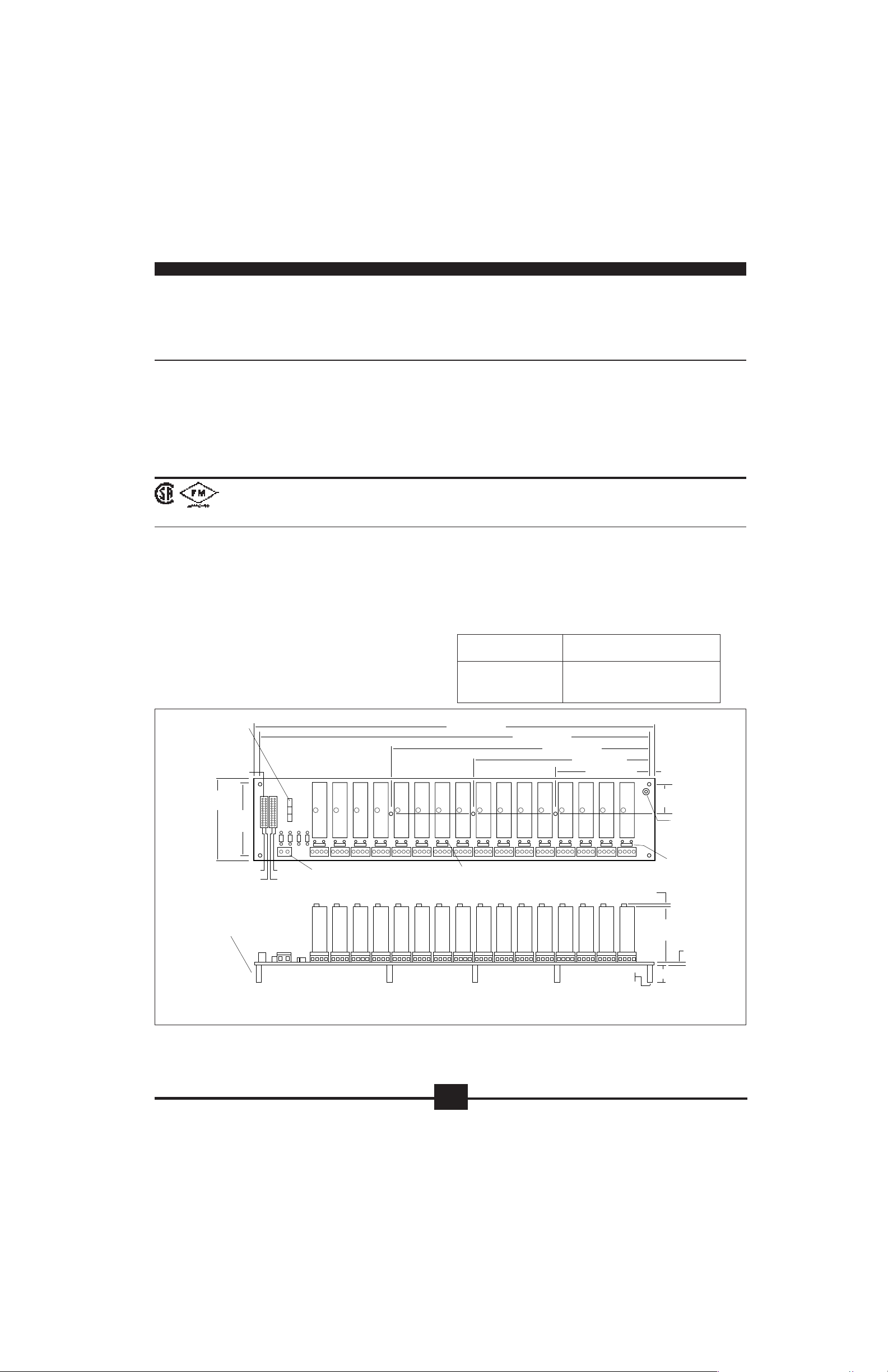
The OM5-BP-16-C 16 channel backpanel (Figure 1) can accept any of the
OM5 analog modules in any mixture. It can be mounted on the OMX-1363-
C 19-inch metal rack. The OM5-BP-16-C has 16 non-addressable analog I/
O signal channels which provides each module with it’s own analog bus. The
module output switch is continuously “on” when using this backpanel and all
sixteen module outputs are simultaneously accessible to high-speed data
acquisition (ADC) boards. A set of inter-channel bridge jumpers permits
connecting an input module’s output to an output module’s input, providing
two levels of isolation. A temperature sensor is mounted on each channel to
provide cold junction compensation for thermocouple input modules (See
● INTERFACE CABLES
● MODULE EVALUATION BOARD
● CABLE-TO-SCREW-TERMINAL INTERFACE BOARD
SCM5B
Figure 2 for schematic). Field connections are terminated with four screw
terminals at each module site. Use system interface cable OMX-1315-XXC for connection to the host system.
SPECIFICATIONS
Operating Temperature: –40°C to +85°C
95% relative humidity, non-condensing
Interface Connector:
Field High Density Screw Clamp, 14 AWG Max
Logic 26-pin, male header connector
FIGURE 1. OM5-BP-16-C Analog I/O Backpanel Dimensions.
35
Page 18

OUTVIN
RD EN\
V
222018
PCOM
+In
+EXC
16
+SEN
642
I/O 1
I/O 2
I/O 3
232119
WR EN\
RD EN\
222018
232119
WR EN\
I/O 4
I/O 5
NC
I/O COM
OUTVIN
V
NC
I/O COM
I/O 6
I/O 12
JP11
I/O 13
JP12
OMX-1362-C
OMX-1362-C
I/O 16
I/O 14
I/O 15
JP13
JP14
JP15
OP16
PCOM
OP1
531
–In
I/O COM
+In
+EXC
642
531
–In
I/O 7
JP6
–EXC
–SEN
+SEN
–EXC
–SEN
I/O 8
JP7
JP8
I/O 9
JP9
I/O 10
I/O 11
JP10
17
+5
16
17
+5
OMX-CJC-C
OMX-CJC-C
1234
TB16
1234
TB1
Channel 16
–EXC +EXC–In +In
Channel 1
–EXC +EXC–In +In
are factory installed.
1
2. OMX-CJC-C are CJC temperature sensors.
3. Resistors OMX-1362-C are optional I/V conversion
NOTES:
1. J1, J3, J4 and R
resistors for current inputs, not factory installed.
JP1
JP2
JP3
JP4
JP5
246810
10
ACOM
hannel
E1
2
ACOM
hannel
3
hannel
HD10
13579
12345678910111213141516171819202122232425
12345678910111213141516171819202122232425
P2 P1
1
9
hannel
hannel
11
ACOM
hannel
246810
HD10
13579
4
12
ACOM
hannel
hannel
5
13
hannel
hannel
E2
14
ACOM
hannel
6
hannel
7
ACOM
hannel
246810
HD10
13579
15
16
ACOM
hannel
hannel
8
hannel
36
Sense
ACOM
E3
PCOM
J4
Jumper
J3
Jumper
26
26
Jumper
J2
Jumper
R
Fuse (4A)
1
J1
F1
+5
DZ1
4 Amps
+5
Signal Ground
and Grounding Bolt
PCOM
5.6V
LED
PCOM
TB17
FIGURE 2. OM5-BP-16-C Schematic.
Page 19

ELECTRICAL
P1
3
6
9
12
15
P2
J3
19
OM5 Module
18
21
24
25
J1
J2
Sense
AGND
Signal Ground
and
Grounding Bolt
R
1
J4
Power Common
16I/O COM PWR COM
P1 AND P2 CONNECTOR
Connection to the host system is made at connectors P1 and P2. These
connectors are electrically equivalent. Two connectors are provided to allow
both analog input and analog output from host systems having individual
input and output connectors.
ADJACENT CHANNEL JUMPERS
Adjacent channels may be connected together to provide an isolated output
signal from an isolated input module, providing two levels of 1500V
isolation. This capability is provided with the 15 jumpers labeled JP1
through JP15 on headers E1, E2, and E3. A simplified drawing of the OM5BP-16-C schematic for Channel 1 through 4 is shown in Figure 3.
Example: Assume an OM5-IMV input module is installed in Channel 1
position and an OM5-IVI output module is installed in Channel 2 position.
If JP1 is installed, the output of Channel 1 is connected to the input of Channel
2, which provides two levels of 1500V isolation.
GROUNDING
Figure 4 details the optional ground jumper configuration available on the
OM5-BP-16-C backpanel. Jumpers J1, J3, and J4 are factory installed.
Jumper J1 connects the AGND shield wires (pins 3, 6, 9, 12, 15, 18, 21, and
24) to the backpanel signal ground. This provides a ground connection
between the host system and backpanel. Jumper J1 is required if output
modules are used, or if there is no high impedance sense input (input low of
a differential or pseudo-differential system) on the host measurement system.
Jumper J3 connects the SENSE line (pin 25) to the backpanel signal ground.
If the host system has the capability, this allows measuring the OM5-BP-16C ground potential.
For proper operation of the output switch or track-and-hold circuit when
using the OM5 backpanels, a current path must exist between the host control
logic power common and module I/O Common (module pin 19). This path
can be established on the OM5-BP-16-C via jumper J4. If this connection
exists elsewhere in the system, jumper J4 should be removed since possible
ground loops could exist. Other connections of power ground and signal
SCM5B
P1
P2
1
5
7
11
13
V
OUT
V
IN
CH 1
JP1 JP2 JP3
12 34 56
20
V
OUT
18
V
CH 2
HD10, E1
20
18
IN
V
OUT
V
CH 3
20
V
18
IN
OUT
CH 4
V
IN
JP4
20
18
FIGURE 3. OM5-BP-16-C Adjacent Channel Jumpers.
POWER
The OM5-BP-16-C backpanel requires external +5VDC ±5% power. The
chassis mounted OMX-976-C power supplies have adequate capacity to
power any combination of modules.
FUSING
The OM5-BP-16-C backpanel power is fuse protected through F1. This is a
Littlefuse type 252004, 4 amp fuse. Zener diode DZ1 provides extra
protection by clamping the input power voltage to +5.6V. If the input supply
voltage connection is reversed, this zener diode will be forward biased and
fuse F1 will be blown.
FIGURE 4. OM5-BP-16-C Grounding Diagram.
ground usually occur at the A/D or D/A converter of the host measurement
system.
If the connection of power common and AGND shield wires exists in the host
measurement system, an optional resistive connection between AGND and
the backpanel signal ground can be made via R1. R1 can be as large as 10K
ohms; 100 ohms is a recommended value. Jumper J2 can be used to connect
the SENSE line to R1 when this ground configuration is used.
For full protection against large electrical disturbances on the field-side of the
OM5 modules, a #10-32 ground stud is provided on the backpanel. An
electrical connection between this ground stud and system ground should be
provided with a large gauge wire of the shortest possible length. When this
connection is made, a possible ground loop could result through the AGND
shield wires and backpanel signal ground. If the application involves only
input modules and a differential input is used by the host measurement
system, J1 should be removed. Remember that J1 is required if output
modules are used or if the host system does not have differential inputs.
37
Page 20

OM5-BP-16-MUX-C 16 POSITION ANALOG I/O BACKPANEL, MULTIPLEXED
DESCRIPTION
The OM5-BP-16-MUX-C 16 channel backpanel (Figure 5) can accept any
of the OM5 analog modules in any mixture. It can be mounted on the
OMX-1363-C 19-inch metal rack. The OM5-BP-16-MUX-C has two
analog buses; one for analog input and one for analog output. This twobus configuration takes advantage of the switch controlled outputs on the
input modules and the track-and-hold inputs on the output modules. A
temperature sensor is mounted on each channel to provide cold junction
compensation for thermocouple input modules (See Figure 6 for
schematic). Field connections are terminated with four screw terminals at
each module site. Up to four OM5-BP-16-MUX-C backpanels may be
daisy-chained. Use OMX-CAB-01-C cable for daisy chaining and OMX1315-XX-C cable for connecting to host computer.
26 Conductor Male
Pin Connector P1
(1)
SPECIFICATIONS
Operating Temperature: –40°C to +85°C
95% relative humidity, non-condensing
Interface Connector:
Field High Density Screw Clamp, 14 AWG Max
Logic 26-pin, male header connector
Address Input Logic Levels:
Max Logic “0” 0.8V
Min Logic “1” 2.0V
II Input Current, “0” or “1” 0.1µA max at 25°C
RD EN\ or WR EN\ Signal Delay
from Connector P1 to Channels 1-16
Standalone (address 0-15) 51ns at 25°C
Expanded (address 16-63) 100ns at 25°C
17.4" (442.0mm)
17.1" (434.3mm)
11.3" (287.0mm)
7.6" (193.0mm)
3.9" (99.1mm)
1.0µA max –25°C to +85°C
64ns at –25°C to +85°C
126ns at –25°C to +85°C
0.15"
(3.8mm)
3.47"
(88.1mm)
(77.5mm)
Read Address
Selection Jumper
Swaged Standoff
Thru Hole 0.15" (3.8mm) Dia.
NOTES:
1. Connector is Berg 65863-075 or equivalent.
Mating Connector is Amp 49958-6 or equivalent.
3.05"
Pin 2
Pin 1
P1
E2
E1
4
3
2
1
0
+5VDC Supply
Channel
Write Address
Selection Jumper
12345678910111213141516
FIGURE 5. OM5-BP-16-MUX-C Analog I/O Backpanel.
Sockets for Current Conversion Resistors, OMX-1362-C
0.14" (3.6mm)
inside diameter
1.275"
(32.4mm)
10.32 X 0.40
Ground Lug, Including
Nut and Lockwasher
OMX-CJC-C
Cold Junction
Compensation Circuit
0.08"
(2.0mm)
2.27"
(57.7mm)
0.093"
(2.4mm)
0.75" (19.1mm)
38
Page 21

OUTVIN
RD EN\
V
222018
PCOM
+In
+EXC
16
+SEN
642
RD16
RD15
791011121314
Y7Y6Y5Y4Y3Y2Y1
U2
G1
G2A
74HCT138
645
RD14
G2B
RD13
RD12
321
RD11
RD10
CBA
RD9
15
Y0
232119
NC
WR EN\
RD EN\
V
222018
232119
NC
WR EN\
U3
17
OP16
+5
I/O COM
PCOM
OUTVIN
+In
16
642
17
OP1
+5
I/O COM
RD8
RD7
RD6
791011121314
Y7Y6Y5Y4Y3Y2Y1
G1
G2A
74HCT138
+5
G2B
645
531
–In
–EXC
+EXC
+SEN
531
–In
–EXC
RD5
RD4
–SEN
–SEN
RD3
RD2
CBA
321
RD1
15
Y0
OMX-CJC-C
OMX-CJC-C
WR16
WR15
791011121314
Y7Y6Y5Y4Y3Y2Y1
U4
G1
G2A
74HCT138
645
OMX-1362-C
OMX-1362-C
WR14
WR13
WR12
WR11
G2B
CBA
321
WR10
WR9
15
Y0
1234
TB16
1234
TB1
Channel 16
–EXC +EXC–In +In
Channel 1
–EXC +EXC–In +In
WR8
791011121314
Y7Y6Y5Y4Y3Y2Y1
U5
G1
74HCT138
645
+5
are factory installed.
1
2. OMX-CJC-C are CJC temperature sensors.
3. Resistors OMX-1362-C are optional I/V conversion
NOTES:
1. J1, J2, J4 and R
WR7
WR6
G2A
G2B
resistors for current inputs, not factory installed.
WR1
WR5
WR4
WR3
WR2
15
Y0
CBA
321
SCM5B
PCOM
J4
Jumper
J2
Jumper
J1
Jumper
Jumper
1
R
J3
Signal Ground
and Grounding Bolt
FIGURE 6. OM5-BP-16-MUX-C Schematic.
43210
HD10
765
4
Y3Y2Y1
U1
G
1
3
R5
B
2
W0W1W2W3W4
74HCT139
OUTVIN
V
12345678910111213141516171819202122232425
P1
ACOM
VREAD
VWRITE
ACOM
SNS LO
R0R1R2R3R4
ACOM
Y0
A
E1
43210
HD10
91011
Y3Y2Y1
U1
G
74HCT139
15
W5
13
RD EN\
WR EN\
E2
12
Y0
B
A
14
N/C
DATA
39
N/C
N/C
26
DCOM
DCOM
Data
Fuse
+5
1
C
+
DZ1
F1
4 Amps
+5
PCOM
5.6V
LED
PCOM
TB17
Page 22

ELECTRICAL
P1 CONNECTOR
The 26 pin P1 connector provides the signal interface between the OM5-BP16-MUX-C backpanel and the host measurement system. Two separate
analog bus connections are provided; one for analog input signals and one
for analog output signals. Two sets of six address lines and an enable pin
allow input and output modules to be independently multiplexed onto their
respective analog signal bus. R0 thru R5 and RDENAB are used for input
modules, and W0 thru W5 and WRENAB are used for output modules.
ADDRESS SELECTION
The OM5-BP-16-MUX-C backpanel has address decoding circuitry to allow
multiplexing any combination of up to 16 input or output modules. Capability
is also provided in the address decode circuitry to expand the system to 64
channels (four OM5-BP-16-MUX-C backpanels) of multiplexed input or
output. Jumpers on HD10 header, E1 and E2 group, select which set of 16
addresses are assigned to a particular backpanel. The E1 group assigns a set
of 16 addresses for input modules, and the E2 group assigns a set of 16
addresses for output modules. The table below shows the correlation of
jumper position to address range.
E1 Jumper Pos E2 Jumper Pos Address Range/Mode
4 4 0-15, STAND ALONE
3 3 48-63, EXPANDED
2 2 32-47, EXPANDED
1 1 16-31, EXPANDED
0 0 0-15, EXPANDED
To connect multiple OM5-BP-16-MUX-C backpanels in this expanded
configuration, use interconnect cable OM5-CAB-01-C.
POWER
The OM5-BP-16-MUX-C backpanel requires external +5VDC ±5% power.
The chassis mounted OMX-976 power supplies have adequate capacity to
power any combination of modules.
FUSING
The OM5-BP-16-MUX-C backpanel power is fuse protected through F1.
This is a Littlefuse type 252004, 4 amp fuse. Zener diode DZ1 provides extra
protection by clamping the input power voltage to +5.6V. If the input supply
voltage connection is reversed, this zener diode will be forward biased and
fuse F1 will be blown.
GROUNDING
Figure 7 below details the optional ground jumper configuration available on
the OM5-BP-16-MUX-C backpanel. Jumpers J1, J2, and J4 are factory
installed.
Jumper J1 connects the SIG COM shield wires (pins 2, 5, and 6) to the
backpanel signal ground. This provides a ground connection between the
host system and backpanel. Jumper J1 is required if output modules are
used, or if there is no high impedance sense input (input low of a differential
or pseudo-differential system) on the host measurement system.
Jumper J2 connects the SNS LO line (pin 4) to the backpanel signal ground.
If the host system has the capability, this allows measuring the OM5-BP-16MUX-C ground potential.
For proper operation of the output switch or track-and-hold circuit when
using the OM5-BP-16 backpanels, a current path must exist between the host
control logic power common and module I/O Common (module pin 19). This
path can be established on the OM5-BP-16-MUX-C via jumper J4. If this
connection exists elsewhere in the system, jumper J4 should be removed
since possible ground loops could exist. Other connections of power ground
and signal ground usually occur at the A/D or D/A converter of the host
measurement system.
If the connection of power common and SIG COM shield wires exist in the
host measurement system, a resistive connection between SIG COM and the
backpanel signal ground can be made via R1. R1 can be as large as 10K ohms;
100 ohms is a recommended value. Jumper J3 can be used to connect the
SNS LO line to R1 when this ground configuration is used.
For full protection against large electrical disturbances on the field-side of the
OM5 modules, a #10-32 ground stud is provided on the backpanel. An
electrical connection between this ground stud and system ground should be
provided with a large gauge wire of the shortest possible length. When this
connection is made, a possible ground loop could result through the SIG
COM shield wires and backpanel signal ground. If the application involves
only input modules and a differential input is used by the host measurement
system, J1 should be removed. Remember that J1 is required if output
modules are used or if the host system does not have differential inputs.
P1
2 SIG COM
5 SIG COM
6 SIG COM
4 SIG COM
J2
J3
J1
R
1
J4
Power Common
Signal Ground
Grounding Bolt
and
OM5 Module
19
16I/O COM PWR COM
FIGURE 7. OM5-BP-16-MUX-C Grounding Diagram.
40
Page 23

OM5-BP-SKT-C /-2-C ONE / TWO POSITION ANALOG I/O BACKPANELS
DESCRIPTION
The OM5-BP-SKT-C is a single channel mounting panel for the OM5
modules. The OM5-BP-2-C is a dual channel mounting panel for the OM5
modules. They both are DIN rail compatible.
See Figures 9 and 10 for wiring diagrams, Figures 11 and 12 for schematics.
The following accessories are required for mounting one OM5-BP-SKT- or
-2-C panel (Figure 8):
Qty Model Description
1 OM7-DIN-SF Base element with snap foot
2 OM7-DIN-SE Side element
The following accessories are required for mounting two or more OM5-BPSKT- or -2-C panels:
Qty Model Description
2 OM7-DIN-SF Base element with snap foot
2 OM7-DIN-SE Side element
(# panels)-2 OM7-DIN-WSF Base element without snap foot
(4 x (# panels))-4 OM7-DIN-CP Connection pins
The following DIN rail styles are available. Specify length in meters (-XX)
EN 50022-35x7.5 (slotted steel)
EN 50035-G32 (slotted steel)
EN 50022-35x15 (slotted steel)
SPECIFICATIONS
Operating Temperature: –40°C to +85°C
95% relative humidity, non-condensing
Interface Connector:
Field High Density Screw Clamp, 14 AWG Max
Logic High Density Screw Clamp, 14 AWG Max
DIN Rail
OM7-DIN-SE
mounts to DIN rails
EN 50022-35x7.5
EN 50022-35x15
EN 50035-G32
OM7-DIN-SF
OM7-DIN-CP
OM7-DIN-WSF
SCM5B
OM7-DIN-SE
Sockets for Current Conversion Resistor, OMX-1362-C
OMX-CJC-C Cold Junction
Compensation Circuit
1234
–EXC
–In/–Out
1.37"
+In/+Out
(34.8mm)
+EXC
Sockets for Current Conversion Resistor, OMX-1362-C
1.37"
(34.8mm)
TB1 TB2
Isolated I/O
OMX-CJC-C Cold Junction
Compensation Circuit
TB1
+EXC
+In/+Out
–In/–Out
–EXC
1234
Channel A
1234
–EXC
–In/–Out
+In/+Out
Isolated I/O
+EXC
Channel B
4.25"
(108mm)
4.25"
(108mm)
FIGURE 8. DIN Rail Mounting Elements.
J1
Power Common
+5V
I/O COM/–I
VIN/V
OUT
IN
/+I
IN
1234
Local I/O
FIGURE 9. OM5-BP03-C Wiring Diagram.
TB3
Power Common
12
+5V
I/O COM/–I
IN
VIN/V
/+IIN CH A
OUT
123
V
/+IIN CH B
IN/VOUT
J2
Local I/O
TB4TB2
FIGURE 10. OM5-BP04-C Wiring Diagram.
41
Page 24

I/O
VIN/
COM/
V
OUT/
–I
PCOM
+5V
+I
IN
IN
TB2 4321
J1
WR EN\
DATA
I/O COM
+5V
–EXC
–SEN
–In
23
21
19
17
5
3
1
22 RD EN\
20 V
OUT
18 V
IN
16 PCOM
+In
6
+EXC
4
+SEN
2
OMX-CJC-C
OMX-1362-C
1234
TB1
–EXC +EXC–In/
–Out
+In/
+Out
FIGURE 11. OM5-BP-SKT-C Schematic.
LED
+5VPCOM
TB3 21
VIN/
/
V
IN
V
/
V
/
OUT
–I
CH A
OUT
–I
IN
IN
CH B
I/O
COM/
–I
IN
TB4 321
*NOTE: OMX-1362-C resistors are
not installed at factory.
LED
WR EN\
DATA
I/O COM
–EXC
–SEN
TB1
–EXC +EXC–In/
J2
23
21
19
17
+5V
5
–In
3
1
OMX-1362-C
1234
–Out
Channel A
+In
+Out
22 RD EN\
20 V
18 V
16 PCOM
6
4
2
OUT
IN
+In
+EXC
+SEN
FIGURE 12. OM5-BP-2-C Schematic.
WR EN\
23
DATA
21
I/O COM
19
17
+5V
5
–In
3
–EXC
1
–SEN
OMX-CJC-COMX-CJC-C
1234
TB2
–EXC +EXC–In
OMX-1362-C
+In
–Out
+Out
Channel B
22 RD EN\
20 V
OUT
18 V
IN
16 PCOM
+In
6
+EXC
4
+SEN
2
42
Page 25

OM5-BP-8-C 8 POSITION ANALOG I/O BACKPANEL, NON-MULTIPLEXED
0.15"
(3.8mm)
10.32 X 0.40
Ground Lug, Including
Nut and Lockwasher
3.47" (88.1mm)
3.05" (79.5mm)
Barrier Strips for
Field Analog Signal
I/O Termination. (8)
Sockets for Current
Conversion Resistors, OMX-1362-C
+5VDC Supply
1.275" (32.4mm)
5.8"
(147.3mm)
JP7
JP1
9.7"
(246.3mm)
9.5"
(241.3mm)
10.0"
(254.0mm)
Tolerance: ±0.020" (±0.50mm)
26 Conductor
Male Pin
Connectors P1, P2
(1)
0.75"
(19.1mm)
2.25"
(57.2mm)
3.15"
(80.2mm)
Swaged
Standoff
Thru Hole
0.15" (3.8mm) Dia.
(6)
NOTES: (1) Connector is Berg 65863-075 or equivalent.
Mating connector is AMP 49958-6 or equivalent.
Connectors P1 and P2 are wired in parallel for
“Daisy Chaining” up to 8 boards.
OMX-CJC-C
Cold Junction
Compensation Circuit
J12
LH
J5
Pin 1
Pin 2
Pin 1
Pin 2
J1 J2 J3
J4
P1 P2
DESCRIPTION
The OM5-BP-8-C analog module mounting board has a capacity of eight
analog input and/or output modules in any combination. It can be mounted
on the OMX-1363-C 19-inch metal rack. A separate analog signal path is
provided for each channel and each channel’s signal is accessible at
redundant 26-pin connectors. The module output switch is continuously
“on” when using this backpanel and all eight module outputs are simultaneously accessible to high-speed data acquistion (ADC) boards.
On-board jumpers permit paralleling two OM5-BP-8-C boards to form a
OM5-BP-16-C equivalent. An additional set of inter-channel bridge jumpers
permits connecting an input module’s output to an output module’s input,
providing two levels of isolation (Figures 13, 14).
Jumpers on the OM5-BP-8-C permit user selection of low (i.e. channels 0-
7) or high (i.e. channels 8-15) addresses.
A temperature sensor is mounted on each channel to provide cold junction
compensation for thermocouple input modules (See Figure 14 for Schematic-
SPECIFICATIONS
Operating Temperature: –40°C to +85°C
95% relative humidity, non-condensing
Interface Connector:
Field High Density Screw Clamp, 14 AWG Max
Logic 26-pin, male header connector
FIGURE 13. OM5-BP-8-C Analog I/O Backpanel.
ELECTRICAL
ADDRESS SELECTION
Module addresses may be selected as low (channels 0-7) or high (channels
8-15) using the sets of 3 pins labeled J5 through J12. Place a jumper over
the two pins closest to the ribbon cable connectors, P1 and P2, to select a low
address (factory configuration) or over the two pins furthest from the ribbon
cable connectors, P1 and P2, to select a high address.
ADJACENT CHANNEL JUMPERS
Adjacent channels may be connected together to provide an isolated output
signal from an isolated input module, providing two levels of 1500V
isolation. This capability is provided with the seven jumpers labeled JP1–
JP7.
43
Page 26

OUTVIN
RD EN\
V
222018
+In
+EXC
+SEN
PCOM
16
642
I/O 2
I/O 1
I/O 3
I/O 4
I/O 5
JP1
JP2
JP3
JP4
JP5
J10
J9
J8
Jumper Selectable
J7
High/Low Channel Address
J6
J5
I/O 1
I/O 2
I/O 3
I/O 4
I/O 5
I/O 6
I/O 6
I/O 7
JP6
J11
I/O 7
!/O 8
JP7
J12
I/O 8
232119
NC
WR EN\
RD EN\
222018
232119
NC
WR EN\
I/O 9
I/O 10
17
+5
I/O COM
OUTVIN
V
16
17
+5
I/O COM
I/O 11
I/O 12
OP8
OP1
I/O 13
I/O 14
531
–In
I/O COM
+In
PCOM
642
531
–In
I/O COM
I/O 15
I/O 16
–EXC
+EXC
+SEN
–EXC
J4
J3
–SEN
–SEN
PCOM
OMX-CJC-C
OMX-1362-C
1234
Channel 8
–EXC +EXC–In +In
TB8
are factory installed.
1
2. OMX-CJC-C are CJC temperature sensors.
3. Resistors OMX-1362-C are optional I/V conversion
resistors for current inputs, not factory installed.
OMX-CJC-C
OMX-1362-C
1234
Channel 1
–EXC +EXC–In +In
NOTES:
1. J1, J3, J4 and R
TB1
1
J1
R
J2
Signal Ground
and Grounding Bolt
NC
Fuse
F1
+5
DZ1
5.6V
4 Amps
PCOM
LED
157
1113171923
248
1014162022
25
369
1215182124
15711131719232481014162022253691215182124
P2 P1
Sense
ACOM
ACOM
ACOM
ACOM
ACOM
Channel 1
Channel 2
Channel 3
Channel 4
Channel 5
Channel 6
Channel 7
Channel 8
Channel 9
Channel 10
Channel 11
Channel 12
Channel 13
Channel 14
Channel 15
Channel 16
44
ACOM
ACOM
26
26
ACOM
+5
PCOM
TB9
FIGURE 14. OM5-BP-8-C Schematic.
Page 27

OM5-BP-8-MUX-C 8 POSITION ANALOG I/O BACKPANEL, MULTIPLEXED
DESCRIPTION
The OM5-BP-8-MUX-C backpanel (Figure 15) can accept up to eight OM5
modules in any combination. It can be mounted on the OMX-1363-C 19-inch
metal rack. The OM5-BP-8-MUX-C has two analog buses; one for analog
input and one for analog output. This two-bus configuration takes advantage
of the switch controlled outputs on the input modules and the track-and-hold
inputs on the output modules. A temperature sensor is mounted on each
channel to provide cold junction compensation for thermocouple input
modules (See Figure 16 for schematic). Field connections are terminated
with four screw terminals at each module site. Up to eight OM5-BP-8-MUXC backpanels may be daisy-chained. Use OMX-CAB-01-C cable for daisy
chaining and OMX-1315-xx-C cable for connecting to host computer.
Jumpers on the OM5-BP-8-MUX-C permit user selection of low (i.e.
channels 0-7) or high (i.e. channels 8-15) addresses.
Tolerance: ±0.020" (±0.50mm)
26 Conductor
Male Pin Connector P1
Swaged
Standoff
Thru Hole
0.15" (3.8mm) Dia.
(6)
0.75"
(19.1mm)
2.25"
(57.2mm)
3.15"
(80.2mm)
(1)
3.47" (88.1mm)
3.05" (77.5mm)
Pin 2
Pin 1
Read Address
Selection Jumper
P2
P3
P1
1
6
J8
L
H
J6
L
H
J4
J1 J2 J3
+5VDC Supply
Write Address
Selection Jumper
(147.3mm)
J7
J5
NOTES: (1) Connector is Berg 65863-075 or equivalent.
SPECIFICATIONS
Operating Temperature: –40°C to +85°C
Interface Connector:
Field High Density Screw Clamp, 14 AWG Max
Logic 26-pin, male header connector
Address Input Logic Levels:
Max Logic “0” 0.8V
Min Logic “1” 2.0V
II Input Current, “0” or “1” 0.1µA max at 25°C
RD EN\ or WR EN\ Signal Delay
from Connector P1 to Channels 0-7
Standalone (address 0-7) 51ns at 25°C
Expanded (address 8-63) 100ns at 25°C
10.0"
(254.0mm)
9.7"
(246.3mm)
9.5"
5.8"
(241.3mm)
Sockets for Current
Conversion Resistors, OMX-1362-C
Mating connector is AMP 49958-6 or equivalent.
95% relative humidity, non-condensing
1.0µA max –25°C to +85°C
64ns at –25°C to +85°C
126ns at –25°C to +85°C
0.15"
(3.8mm)
10.32 X 0.40
Ground Lug, Including
Nut and Lockwasher
OMX-CJC-C
Cold Junction
Compensation Circuit
Barrier Strips for
Field Analog Signal
I/O Termination. (8)
1.275" (32.4mm)
FIGURE 15. OM5-BP-8-MUX-C Analog I/O Backpanel.
ELECTRICAL
ADDRESS SELECTION
Module read and write addresses may be selected as low (channels 0-7) or
high (channels 8-15) using the four sets of 3 position jumpers labeled J5
through J8. Place a jumper over the two pins furthest from the field I/O
termination blocks on all four sets to select a low address (factory configuration) or over the two pins closest to the field I/O termination blocks on all
four sets to select a high address.
The OM5-BP-8-MUX-C backpanel has address decoding circuitry to allow
multiplexing any combination of up to 8 input or output modules. Capability
is also provided in the address decode circuitry to expand the system to 64
channels (eight OM5-BP-8-MUX-C backpanels) of multiplexed input or
output. Jumpers select which set of 16 addresses are assigned to a particular
backpanel. The Read Address group assigns a set of 16 addresses for input
modules, and the Write Address group assigns a set of 16 addresses for
output modules. The table below shows the correlation of jumper position to
address range.
Address Selection Jumpers
Read Address Write Address Address
Jumper ( P2) Jumper(P3) Range
1 6 0-15 Stand alone
2 7 48-63 Expanded
3 8 32-47 Expanded
4 9 16-31 Expanded
5 10 0-15 Expanded
45
Page 28

OUTVIN
RD EN\
V
222018
+In
+EXC
+SEN
PCOM
16
642
232119
NC
WR EN\
RD EN\
V
222018
232119
NC
WR EN\
OUTVIN
17
OP8
+5
I/O COM
+In
PCOM
16
642
17
OP1
+5
I/O COM
RD8
RD7
791011121314
Y7Y6Y5Y4Y3Y2Y1
U2
G1
74HCT138
645
531
–In
–EXC
+EXC
+SEN
531
–In
–EXC
RD6
G2A
G2B
–SEN
–SEN
RD5
RD4
RD3
RD2
CBA
321
RD1
15
Y0
OMX-CJC-C
OMX-CJC-C
U3
OMX-1362-C
OMX-1362-C
WR8
WR7
WR6
791011121314
Y7Y6Y5Y4Y3Y2Y1
G1
G2A
74HCT138
645
G2B
1234
TB8
1234
TB1
WR5
–EXC +EXC–In+In
–EXC +EXC–In+In
WR4
WR3
321
Channel 8
Channel 1
WR2
WR1
15
Y0
CBA
are factory installed.
1
2. OMX-CJC-C are CJC temperature sensors.
3. Resistors OMX-1362-C are optional I/V conversion
NOTES:
1. J1, J2, J4 and R
resistors for current inputs, not factory installed.
J4
J2
OUTVIN
V
12345
P1
VREAD
PCOM
J1
J3
ACOM
VWRITE
1
R
ACOM
SNS LO
Signal Ground
and Grounding Bolt
U1
1/2
6
ACOM
Jumper Selectable
12345
P2
74LS139
19
RD EN\
J6
Address
Low High
High/Low Channel
+5V
765
4
Y3Y2Y1
G
1
Y0
B
A
3
2
12111098
R5R4R3R2R1
7
R0
J5
High/Low Channel
Jumper Selectable
Address
Low High
J8
J7
+5V
678
1/2
U1
74LS139
20
WR EN\
P3
91011
Y3Y2Y1
G
15
1817161514
W5W4W3W2W1
9
10
12
Y0
B
A
13
14
Fuse
NC
NC
Data
13
2223242526
W0
Data
DCOM
DCOM
F1
+5
1
C
+
DZ1
5.6V
4 Amps
+5
PCOM
LED
PCOM
TB9
FIGURE 16. OM5-BP-8-MUX-C Schematic.
46
Page 29

OM5-BP-16-DIN-C, OM5-BP-16-MUX-DIN-C, OM5-BP-8-DIN-C,
OM5-BP-8-MUX-DIN-C
DESCRIPTION
SCMXSE DIN rail mounting elements. The SCMPB0X-2 comes fully as-
sembled.
The SCMPB0X-2 is the SCMPB0X backpanel with a DIN rail mounting
option. The SCMPB0X backpanel is attached to a 0.062" thick piece of black
anodized aluminum, which in turn is captured using the SCMXBEFE and
OMX-1363-C 19 INCH METAL MOUNTING RACK
DESCRIPTION
The OMX-1363-C is a 19-inch metal rack for mounting the OM5-BP backpanels. It also provides capability to mount the PMX-976-C power supplies, and
the OMX-1324-C interface board (See Figure 17 for dimensions).
17.60" (447.04mm)
3.62" (91.95mm)
3.12" (79.25mm)
0.31" (7.87mm)
1.375" (34.93mm) 2 PL
0.062" (1.57mm)
0
0.63"
(16.00mm)
3.480" (88.39mm)
3.378" (85.80mm)
3.103" (78.82mm)
0.125" (3.17mm) 2 PL
0
0.141" (3.58mm) Dia 8 PL
17.29"
(439.16mm)
18.23"
(463.04mm)
3.265
(82.93mm)
Cable Access Cutout
Left Side Only
3.00"
(76.2mm)
SCM5B
3mm metric
0.378" (9.60mm)
0.103" (2.62mm)
PEM nut 7 PL
0
0.215"
(5.46mm)
0
0 1.10"
(27.94mm)
2.60"
(66.04mm)
0.50"
(12.7mm)
FIGURE 17. OMX-1363-C Analog Rack Dimensions.
OMX-1324-C UNIVERSAL INTERFACE BOARD
DESCRIPTION
The OMX-1324-C is a universal interface board which converts a 26-pin ribbon cable input to 26 screw terminals for discrete wire. It can be mounted on
the back of the OMX-1363-C mounting rack or on a DIN rail. Required mounting hardware is included. Use OMX-1315-xx-C cable (See Figure 18 for
dimensions).
2468101214161820222426
135791113151719212325
4.00"
(101.6mm)
2
1
2.20"
(55.9mm)
1.90"
(48.3mm)
FIGURE 18. OMX-1324-C Universal Interface Board Dimensions.
47
Page 30

OM5-BP-SKT-C ANALOG MODULE EVALUATION BOARD
DESCRIPTION
The OM5-BP-SKT-C is a single channel board with a test socket for OM5
module evaluation (Figure 19). All signal input/output, control, and power
connections are connected to terminal blocks for ease of user access. A cold
junction temperature sensor circuit is included for evaluation of thermocouple modules. (See Figure 20 for schematic).
The OM5-BP-SKT-C is mechanically compatible with DIN rail mounting
using the following elements:
2 OM7-DIN-SF base elements with snap foot
2 OM7-DIN-SE side elements
4 OM7-DIN-CP connection pins
Two jumpers are provided for customer use. The first, J1, provides a current
path between +5V Power Common (module pin 16) and I/O Common
(module pin 19). A path must exist between the host control logic power
common and module I/O Common for proper operation of the module output
switch or track-and-hold circuit. If this connection exists elsewhere in the
system, jumper J1 should be removed since possible ground loops could
exist. Other connections of power ground and signal ground usually occur
at the A/D or D/A converter of the host measurement system.
Jumper J2 is used in the cold junction compensation circuit. If it is installed,
the compensation circuit is enabled and will provide the proper compensation voltage to correct for the thermoelectric effect at the +In and –In screw
terminals. If an external simulation voltage is desired for cold junction
compensation, J2 should be removed. The external voltage is applied at the
sockets labled CJC+ and CJC–. An external voltage of 510.0 mV corresponds
to an ambient temperature of +25 °C. The transfer function of the onboard
compensation circuit is V
= 0.510 –0.0025(T–25)V.
CJC
2.85"
(72.4mm)
V
OUT
I/O COM
V
IN
I/O COM
J1
+
CJC
–
J2
OMX-1362-C
OMX-CJC-C
TB4
–In
+EXC
+In
4.25"
(108mm)
0.25"
(6.4mm)
Typical
Reserved
0.25" (6.4mm) Typical
Control Local I/O
RD EN\
WR EN\
PCOM
TB1 TB2
+5V
PCOM
TB3
–EXC
FIGURE 19. OM5-BP-SKT-C Evaluation Board Dimensions And Pin Layout.
TB1
RD EN\
WR EN\
Reserved
PCOM
PCOM
TB3
NOTES:
1. J1 and J2 are factory installed.
2. SCMXCJC is a CJC temperature sensor.
3. Resistor SCMXR1 is an optional I/V conversion
resistor for current inputs, not factory installed.
+5
PCOM
DZ1
LED
PCOM
FIGURE 20. OM5-BP-SKT-C Evaluation Board Schematic.
I/O COM
TB4
23
21
19
17
–In 5
–EXC 3
–SEN 1
J2
OMX-CJC-C
OMX-1362-C
–EXC +EXC–In +In
OM5
22
20
18
16
6 +In
4 +EXC
2 +SEN
PCOM
+
CJC
–
TB2
J1
PCOM
V
OUT
I/O COM
V
IN
I/O COM
I/O COM
48
Page 31

OM5-1315-XX-C, OMX-CAB-01-C INTERFACE CABLES
DESCRIPTION
OM5-1315-XX-C
System interface cable for the SCMPB01/02/05/06 backpanels. This is a 26
conductor ribbon cable with a mass-terminated socket connector installed on
each end. It can be ordered in any length; -xx denotes required length in
meters (Figure 21).
OMX-CAB-01-C
Daisy-chain cable provides interconnection between a maximum of four
OM5-BP-16-MUX-C and eight OM5-BP-8-MUX-C backpanels (See Figure
22).
Colored Stripe on
Cable is Assembled to
Pin 1 of Connectors
Pin 1
Pin Connector
Pin 1
1 Meter (3.3 feet)
Socket
Connector
Colored Stripe on
Cable is Assembled to
Pin 1 of Connectors
Pin 1
–XX, Lenglth in Meters
Cable
Socket
Connector
Pin 1
Socket
Connector
FIGURE 21. OMX-1315-XX-C System Interface Cable. FIGURE 22. OMX-CAB-01-C Daisy-Chain Cable.
OMX-CAB-01-C
OMX-CAB-01-C
OM5-BP-8 or 16-MUX-C
OM5-BP-8 or 16-MUX-C
Cable
Socket
Connector
Pin 1
SCM5B
OMX-CAB-01-C
TO HOST
SYSTEM
OMX-1315-XX-C
FIGURE 23. Application Of OMX-CAB-01-C Daisy-Chain Cable.
OM5-BP-8 or 16-MUX-C
OM5-BP-8 or 16-MUX-C
Up to eight OM5-BP-8-MUX-C backpanels
49
Page 32

OMX-CJC-C ENCAPSULATED COLD JUNCTION COMPENSATION
0.60"
(15.2mm)
0.30"
(7.6mm)
0.50"
(12.7mm)
0.10" – 0.15"
(2.5 – 3.8mm)
0.03" (0.76mm)
0.15" (3.8mm)
0.35" (8.9mm)
0.45" (11.4mm)
Bottom
–SEN +SEN–EXC
Pin Width = 0.020" (0.51mm)
(Recommended PCB
hole size of 0.031")
Side Side
0.50"
(12.7mm)
0.50"
(12.7mm)
0.075"
(1.9mm)
0.05" (1.3mm)
0.45" (10.2mm)
Bottom
Pin Width = 0.040" (1.02mm)
Side Side
0.15"
(3.8mm)
DESCRIPTION
The OMX-CJC-C is the identical circuit used on the OM5-BP backpanels
except it is packaged as a component for use in customer designed mounting
boards (Figure 24). When interfaced to an OM5-ITC or OM5-LTC module, the
transfer function of the voltage across the +SEN and –SEN pins is V
–0.0025(T –25)V.
= 0.510
CJC
SPECIFICATIONS
Accuracy +25°C ±0.25°C
+5°C to +45°C ±0.5°C
–40°C to +85°C ±1.25°C
FIGURE 24. OMX-CJC-C Physical Dimensions And Pin Layout.
OMX-1344 JUMPERS
DESCRIPTION
Package of 10 jumpers for connecting adjacent input/output modules on the OM5-BP-16-C backpanel. This connection is made if it is desired to direct
the output of any input module to the input of an adjacent output module. The jumpers can also be used for configuring I/O addresses on the OM5-BP16-MUX-C backpanel.
OMX1362-C CURRENT CONVERSION RESISTOR
DESCRIPTION
A precision 20Ω, 0.1%, 10ppm/°C resistor used with the OM5-II current
input module or OM5-TX two-wire transmitter interface module (Figure 25).
Sockets are provided on all backpanels to allow installation of this resistor.
One OMX-1362-C is shipped with each module.
FIGURE 25. OMX-1362-C Physical Dimensions.
50
Page 33

OMX-955-C, OMX-955-220-C POWER SUPPLIES
DESCRIPTION
The OMX-955-C encapsulated power supplies are available in 120VAC or
220VAC input voltage ranges and provide 5VDC outputs suitable for all OM5
modules. They are designed to mount on the OMX-1363-C metal rack. The
supplies are UL-recognized and CSA certified. Their compact size and low
weight are ideal for high-density applications (see Figure 25.)
SPECIFICATIONS
OMX-955-C OMX -955-220-C
Input Voltage Range 105-125VAC 200-240VAC
Output Voltage 5VDC 5VDC
Output Current, +50°C1A1A
(derate 2.5%/°C above +50°C)
Operating Temp -25°C to +71°C -25°C to +71°C
Dielectric Withstand Voltage (Input to Ground) 2500VRMS 2500VRMS
Line Regulation ±0.05% ±0.05%
Load Regulation ±0.15% ±0.15%
Output Ripple, max 2mVRMS 2mVRMS
Overvoltage Protection, nominal 6.2V 6.2V
Weight 1.25 lbs (567 grams) 1.25 lbs (567 grams)
Supplies are UL recognized, File No. E65890, and CSA certified, File No. LR59996.
0.75"
(19.1mm)
5.40 BH
Screws
0.75"
(19.1mm)
AC
AC
SCM5B
Inserts
4.40 Thread
.125" (3.2mm) deep
2.00" (50.8mm)
2.70" (68.6mm)
FIGURE 25. OMX-955/955-220-C Physical Dimensions.
2.50"
(63.5mm)
0.35"
(8.9mm)
4.00"
(101.6mm)
NC
NC
COM
+OUT
1.45" (36.8mm)
51
Page 34

OMX-977-C, OMX-977-220-C POWER SUPPLIES
DESCRIPTION
The OMX-977 Linear Power Supplies are available in 120VAC or 220VAC
input. They have sufficient output current capacity to supply any combination
of OM5 modules. The OMX-1363-C metal rack provides mounting capability
for the power supplies (See Figure 26).
SPECIFICATIONS
OMX-977-C OMX-977-220-C
Input Voltage Range 104-132VAC 207-265VAC
Output Voltage 5VDC±1% 5VDC±1%
Output Current (at +70°C) 3A 3A
Output Current (at +50°C) 6A 6A
Operating Temp 0 to +70°C 0 to +70°C
Dielectric Withstand Voltage (input to ground) 3750VAC 3750VAC
Line Regulation (10% line change) ±0.05% ±0.05%
Load Regulation (50% load change) ±0.05% ±0.05%
Output Ripple (max) 5 mV
Overvoltage Protection (factory set) 6.2 V ± 0.4V 6.2 V ± 0.4V
Both supplies are tested and certified by TUV to VDE 0806 and IEC 380. They are UL Recognized (File Number E55974) and CSA Certified
(CSA File Number LR38879).
P-P
5 mV
P-P
Side Side
0.05" (1.3mm)
0.45" (10.2mm)
Bottom
FIGURE 26. OMX-977/977-220-C Physical Dimensions.
0.50"
(12.7mm)
0.15"
(3.8mm)
0.50"
(12.7mm)
0.075"
(1.9mm)
Pin Width = 0.040" (1.02mm)
52
Page 35

General Description
OMEGA® OM5 Series Isolated Signal Conditioning Modules are low cost,
high performance, plug-in signal conditioners. Each OM5 module provides
a single channel of isolated analog input or output. Input modules interface
to all types of external sensors. The modules filter, isolate, amplify, and
convert the input signal to a high-level analog voltage output. The output
modules accept a high-level analog voltage signal from a host system, then
buffer, isolate, and amplify before providing a process current or voltage
output to field devices. Over 115 different OM5 modules are available
encompassing a wide selection of isolated analog input and output functions.
Analog inputs include voltage and current in narrow and wide bandwidths,
Thermocouple, RTD, Potentiometer, Strain Gage, Frequency, and 2-Wire
Transmitter. Custom I/O ranges are also available. All modules are CSA
certified and FM approved for safe operation in Class I, Division 2, Groups
A, B, C, and D hazardous environments.
Accessories include: addressable and non-addressable single, dual, eight
and 16 channel backpanels, available with on-board temperature sensors
and cold junction thermocouple compensation; power supplies; mounting
racks; interface cables, and evaluation boards.
OM5 modules offer several advantages when compared with competitive
parts, while maintaining equivalent price:
• 50 times better noise rejection by using a 6-pole filter with 95dB
NMR, versus a three-pole filter with 60dB NMR; • Lower output noise
• True 3-way isolation • CMR of noise spikes measures 20dB better
than competing models.
Key Specifications
• 1500V Isolation
• Accuracy, 0.05%
• CMR, 160dB
• NMR, 95dB
• Transient Protection, ANSI/IEEE C37.90.1-1989
• ±1µV/°C Drift
• Output noise as low as 150µVrms
• 240VAC Protection for field I/O
• Operating temp range, –40°C/+85°C
• CSA CERTIFIED (Class I, Division 2, Groups A, B, C, D)
• FM APPROVED (Class I, Division 2, Groups A, B, C, D)
• EUROPEAN EMC DIRECTIVE COMPLIANT
• CE APPROVAL for low voltage directive not applicable.
Products comply with ENG1010-1 (IEC1010)
Applications
• DESIGNED FOR INDUSTRIAL PLANT ENVIRONMENTS
• PROTECTS USER EQUIPMENT FROM LIGHTNING AND HEAVY
EQUIPMENT POWER-LINE VOLTAGE
• REDUCES ELECTRICAL NOISE IN MEASURED SIGNALS
• CONVENIENT SYSTEM EXPANSION AND REPAIR
SELECTION GUIDE FOR OM5 ISOLATED
SIGNAL CONDITIONING PRODUCTS
ANALOG VOLTAGE INPUT MODULES, NARROW BANDWIDTH (4Hz BW)
MODEL INPUT RANGE OUTPUT RANGE*
OM5-IMV-10A-C ±10mV ±5V
OM5-IMV-50A-C ±50mV ±5V
OM5-IMV-100A-C±100mV ±5V
OM5-IMV-10B-C ±10mV 0 to +5V
OM5-IMV-50B-C ±50mV 0 to +5V
OM5-IMV-100B-C±100mV 0 to +5V
OM5-IV-1A-C ±1V ±5V
OM5-IV-5A-C ±5V ±5V
OM5-IV-10A-C ±10V ±5V
OM5-IV-1B-C ±1V 0 to +5V
OM5-IV-5B-C ±5V 0 to +5V
OM5-IV-10B-C ±10V 0 to +5V
OM5-IV-20A-C ±20V ±5V
OM5-IV-20B-C ±20V 0 to +5V
OM5-IV-40A-C ±40V ±5V
OM5-IV-40B-C ±40V 0 to +5V
ANALOG CURRENT INPUT MODULES, 4Hz AND 1kHz BANDWIDTH
MODEL INPUT RANGE OUTPUT RANGE* BW
OM5-II-4/20-C 4 to 20mA 0 to +5V 4Hz
OM5-II-0/20-C 0 to 20mA 0 to +5V 4Hz
TRUE RMS INPUT MODULES
MODEL INPUT RANGE (rms) OUTPUT RANGE (dc)
OM5-IAC-100B-C 0 to 100mV 0 to +5V
OM5-IAC-1B-C 0 to 1V 0 to +5V
OM5-IAC-10B-C 0 to 10V 0 to +5V
LINEARIZED 2- OR 3-WIRE RTD INPUT MODULES (0 to +5V OUTPUT*,
4Hz BW)
MODEL TYPE*** INPUT RANGE
OM5-IP-N100-C 100Ω Pt –100°C to +100°C (–148°F to +212°F)
OM5-IP-100-C 100Ω Pt 0°C to +100°C (+32°F to +212°F)
OM5-IP-200-C 100Ω Pt 0°C to +200°C (+32°F to +392°F)
OM5-IP-600-C 100Ω Pt 0°C to +600°C (+32°F to +1112°F)
OM5-IC-120-01-C 10Ω Cu at 0°C0°C to +120°C (+32°F to +248°F)
OM5-IC-120-02-C 10Ω Cu at 25°C0°C to +120°C (+32°F to +248°F)
OM5-IN-300-C 120Ω Ni 0°C to +300°C (+32°F to +572°F)
LINEARIZED 4-WIRE RTD INPUT MODULES (0 to +5V OUTPUT*, 4Hz BW)
MODEL TYPE*** INPUT RANGE
OM5-IP4-N100-C 100Ω Pt –100°C to +100°C (–148°F to +212°F)
OM5-IP4-100-C 100Ω Pt 0°C to +100°C (+32°F to +212°F)
OM5-IP4-200-C 100Ω Pt 0°C to +200°C (+32°F to +392°F)
OM5-IP4-600-C 100Ω Pt 0°C to +600°C (+32°F to +1112°F)
OM5-IC4-120-01-C 10Ω Cu at 0°C0°C to +120°C (+32°F to +248°F)
OM5-IC4-120-02-C 10Ω Cu at 25°C0°C to +120°C (+32°F to +248°F)
OM5-IN4-300-C 120Ω Ni 0°C to +300°C (+32°F to +572°F)
POTENTIOMETER INPUT MODULES (4Hz BW)
MODEL INPUT RANGE OUTPUT RANGE*
OM5-PT-100-C 0 to 100Ω 0 to +5V
OM5-PT-500-C 0 to 500Ω 0 to +5V
OM5-PT-1K-C 0 to 1KΩ 0 to +5V
OM5-PT-10K-C 0 to 10KΩ 0 to +5V
THERMOCOUPLE INPUT MODULES (0 to +5V OUTPUT*, 4Hz BW)
MODEL TYPE** INPUT RANGE
OM5-ITC-J-C J –100°C to +760°C (–148°F to +1400°F)
OM5-ITC-K-C K
OM5-ITC-T-C T –100°C to +400°C (–148°F to +752°F)
OM5-ITC-E-C E 0°C to +900°C (+32°F to +1652°F)
OM5-ITC-R-C R 0°C to +1750°C (+32°F to +3182°F)
OM5-ITC-S-C S 0°C to +1750°C (+32°F to +3182°F)
OM5-ITC-B-C B 0°C to +1800°C (+32°F to +3272°F)
OM5-ITC-C1-C C +350°C to +1300°C (+662°F to +2372°F)
OM5-ITC-N1-C N -100°C to +1300°C (-148°F to +2372°F)
STRAIN GAGE INPUT MODULES (
MODEL INPUT EXCITATION
OM5-WBS38-01-C ±10mV Full Bridge Input, (3mV/V) 100 to 10kΩ 3.333V
OM5-WBS-1-C ±30mV Full Bridge Input, (3mV/V) 300 to 10KΩ 10.000V
OM5-WBS38-03-C ±10mV Half Bridge Input, (3mV/V) 100 to 10kΩ 3.333V
OM5-WBS-3-C ±30mV Half Bridge Input, (3mV/V) 300 to 10KΩ 10.000V
OM5-WBS-2-C ±20mV Full Bridge Input, (2mV/V) 300 to 10KΩ 10.000V
OM5-WBS-4-C ±33.3mV Full Bridge Input, (10mV/V) 100 to 10KΩ 3.333V
OM5-WBS-5-C ±100mV Full Bridge Input, (10mV/V) 300 to 10KΩ 10.000V
ANALOG CURRENT OUTPUT MODULES, 400Hz AND 1kHz BANDWIDTH
MODEL INPUT RANGE OUTPUT RANGE BW
OM5-IVI-B4-C 0 to +5V 4 to 20mA 400Hz
OM5-IVI-A4-C ±5V 4 to 20mA 400Hz
OM5-IVI-B0-C 0 to +5V 0 to 20mA 400Hz
OM5-IVI-A0-C ±5V 0 to 20mA 400Hz
–100°C to +1350°C (–148°F to +2462°F)
±5V OUTPUT*, 10kHz BW)
SCM5B
2
Page 36

SELECTION GUIDE FOR OM5 ISOLATED SIGNAL CONDITIONING PRODUCTS
ANALOG VOLTAGE INPUT MODULES, WIDE BANDWIDTH (10kHz BW)
MODEL INPUT RANGE OUTPUT RANGE*
OM5-WMV-10A-C ±10mV ±5V
OM5-WMV-50A-C ±50mV ±5
OM5-WMV-100A-C ±100mV ±5V
OM5-WMV-10B-C ±10mV 0 to +5V
OM5-WMV-50B-C ±50mV 0 to +5V
OM5-WMV-100B-C ±100mV 0 to +5V
OM5-WV-1A-C ±1V ±5V
OM5-WV-5A-C ±5V ±5V
OM5-WV-10A-C ±10V ±5V
OM5-WV-1B-C ±1V 0 to +5V
OM5-WV-5B-C ±5V 0 to +5V
OM5-WV-10B-C ±10V 0 to +5V
OM5-WV-20A-C ±20V ±5V
OM5-WV-20B-C ±20V 0 to +5V
OM5-WV-40A-C ±40V ±5V
OM5-WV-40B-C ±40V 0 to +5V
2-WIRE TRANSMITTER INTERFACE MODULES (100Hz BW)
MODEL INPUT RANGE OUTPUT RANGE
OM5-TX-1-C 4 to 20mA +1 to +5V
OM5-TX-2-C 4 to 20mA +2 to +10V
GENERAL PURPOSE INPUT MODULES, DC EXCITATION
MODEL MAXIMUM INPUT OUTPUT*
OM5-DT-1-C ±1V ±5V
OM5-DT-2-C ±2V ±5V
OM5-DT-3-C ±3V ±5V
OM5-DT-4-C ±4V ±5V
OM5-DT-5-C ±5V ±5V
OM5-DT-6-C ±6V ±5V
OM5-DT-7-C ±7V ±5V
OM5-DT-8-C ±8V ±5V
OM5-DT-9-C ±9V ±5V
OM5-DT-10-C ±10V ±5V
FREQUENCY INPUT MODULES
MODEL INPUT RANGE OUTPUT RANGE*
OM5-IFI-500-C 0 to 500Hz 0 to +5V
OM5-IFI-1K-C 0 to 1kHz 0 to +5V
OM5-IFI-3K-C 0 to 3kHz 0 to +5V
OM5-IFI-5K-C 0 to 5kHz 0 to +5V
OM5-IFI-10K-C 0 to 10kHz 0 to +5V
OM5-IFI-25K-C 0 to 25kHz 0 to +5V
OM5-IFI-50K-C 0 to 50kHz 0 to +5V
OM5-IFI-100K-C 0 to 100kHz 0 to +5V
LINEARIZED THERMOCOUPLE INPUT MODULES (0 to +5V OUTPUT*,
4Hz BW)
MODEL TYPE** INPUT RANGE
OM5-LTC-J1-C J 0°C to +760°C (+32°F to +1400°F)
OM5-LTC-J2-C J –100°C to +300°C (–148°F to +572°F)
OM5-LTC-J3-C J 0°C to +500°C (+32°F to +932°F)
OM5-LTC-J4-C J –100°C to +760°C (–148°F to +1400°F)
OM5-LTC-K1-C K 0°C to +1000°C (+32°F to +1832°F)
OM5-LTC-K2-C K 0°C to +500°C (+32°F to +932°F)
OM5-LTC-K3-C K –100°C to +1350°C (–148°F to +2462°F)
OM5-LTC-K4-C K 0°C to +1200°C (+32°F to +2192°F)
OM5-LTC-T1-C T –100°C to +400°C (–148°F to +752°F)
OM5-LTC-T2-C T 0°C to +200°C (+32°F to +392°F)
OM5-LTC-E-C E 0°C to +1000°C (+32°F to +1832°F)
OM5-LTC-R-C R
OM5OM5-
LTC-S-C
LTC-B-C
S +500°C to +1750°C (+932°F to +3182°F)
B +500°C to +1800°C (+932°F to +3272°F)
+500°C to +1750°C (+932°F to +3182°F)
VOLTAGE OUTPUT MODULES, 50mA DRIVE CAPACITY (400 Hz BW)
MODEL INPUT RANGE OUTPUT RANGE
OM5-AV-1-C 0 to +5V ±5V
OM5-AV-2-C ±5V ±5V
OM5-AV-3-C ±5V 0 to +5V
OM5-AV-4-C 0 to +10V ±10V
OM5-AV-5-C ±10V ±10V
OM5-AV-6-C ±10V 0 to +10V
OM5-AV-7-C ±5V ±10V
ACCESSORIES
MODEL DESCRIPTION
OM5-BP-16-C Non-multiplexed, 16 channel backpanel
OM5-BP-16-DIN-C OM5-BP-16-C with DIN rail mounting option
OM5-BP-16-MUX-C Multiplexed, 16 channel backpanel
OM5-BP-16-MUX-DIN-C OM5-BP-16-MUX-C with DIN rail mounting option
OM5-BP-8-C Non-multiplexed, 8 channel backpanel
OM5-BP-8-DIN-C OM5-BP-8-C with DIN rail mounting option
OM5-BP-8-MUX-C Multiplexed, 8 channel backpanel
OM5-BP-8-MUX-DIN-C OM5-BP-8-MUX-C with DIN rail mounting option
OM5-BP-SKT-C Single channel backpanel, DIN rail mount
OM5-BP-2-C Dual channel backpanel, DIN rail mount
OM7-DIN-WSF Base element without snap foot
OM7-DIN-SF Base element with snap foot
OMX-1315-xx-C System interface cable for analog backpanels
OMX-CAB-01-C Daisy chain cable for OM5-BP-16-MUX-C
OMX-1324-C Ribbon cable to screw interface board
OMX-1344-C Package of 10 jumpers
OMX-955-C Power supply, 1A, 5VDC, 120VAC U.S.
OMX-977-C Power supply, 3A, 5VDC, 120VAC U.S.
OMX-977-220-C Power supply, 3A, 5VDC, 220VAC U.S.
OMX-1362-C Precision 20Ω resistor for OM5-II and OM5-TX
OMX-CJC-C Encapsulated cold junction circuit
OMX-1363-C 19 inch metal rack for mounting backpanels
OM7-DIN-SE Side element
OM7-DIN-CP Connection pins
*Note:
Any module not shown with a 10V output can be specified with 10V output.
Consult factory for minimum quantity and pricing details and module
specifications.
**THERMOCOUPLE ALLOY COMBINATIONS
TYPE MATERIAL
J Iron vs. Copper-Nickel
K Nickel-Chromium vs. Nickel-Aluminum
T Copper vs. Copper-Nickel
E Nickel-Chromium vs. Copper-Nickel
R Platinum-13% Rhodium vs. Platinum
S Platinum-10% Rhodium vs. Platinum
B Platinum-30% Rhodium vs.Platinum-6%Rhodium
C Tungsten-5% Rhenium vs. Tungsten-26% Rhenium
N Nickel-14.2% Chromium-1.4% Silicon vs. Nickel-4.4%
***RTD ALPHA COEFFICIENTS
TYPE ALPHA COEFFICIENT
100Ω Pt 0.00385
120Ω Ni 0.00672
10Ω Cu 0.004274
xx = length in meters
Silicon-0.1% Magnesium
3
Page 37

OM5-IMV/IV
Analog Voltage Input Modules, Narrow Bandwidth
FEATURES
● ACCEPTS MILLIVOLT AND VOLTAGE LEVEL SIGNALS
● HIGH LEVEL VOLTAGE OUTPUTS
● 1500Vrms TRANSFORMER ISOLATION
●
ANSI/IEEE C37.90.1-1989 TRANSIENT PROTECTION
● INPUT PROTECTED TO 240VAC CONTINUOUS
● 160dB CMR
● 95dB NMR AT 60Hz, 90dB at 50Hz
● ±0.05% ACCURACY
● ±0.02% LINEARITY
● ±1µV/°C DRIFT
● CSA CERTIFIED, FM APPROVED, CE COMPLIANT
● MIX AND MATCH OM5 TYPES ON BACKPANELS
DESCRIPTION
Each OM5-IMV and OM5-IV voltage input module provides a single
channel of analog input which is filtered, isolated, amplified, and converted
to a high level analog voltage output (Figure 1). This voltage output is
logic-switch controlled, allowing these modules to share a common analog
bus without the requirement of external multiplexers.
The OM5 modules are designed with a completely isolated computer side
circuit which can be floated to ±50V from Power Common, pin 16. This
complete isolation means that no connection is required between I/O
Common and Power Common for proper operation of the output switch. If
desired, the output switch can be turned on continuously by simply
connecting pin 22, the Read-Enable pin to I/O Common, pin 19.
Signal filtering is accomplished with a six-pole filter which provides 95dB
of normal-mode-rejection at 60Hz and 90dB at 50Hz. Two poles of this filter
are on the field side of the isolation barrier, and the other four are on the
computer side.
After the initial field-side filtering, the input signal is chopped by a
proprietary chopper circuit. Isolation is provided by transformer coupling,
again using a proprietary technique to suppress transmission of common
mode spikes or surges. The module is powered from +5VDC, ±5%.
A special input circuit on the OM5-IMV and OM5-IV modules provides
protection against accidental connection of power-line voltages up to
240VAC.
4
NC
6
5
3
NC
V
IN
+EXC
–EXC
+In
–In
Backpanel
Term Block
4
3
2
1
FIGURE 1. OM5-IMV/IV Block Diagram.
Surge
Suppression
and
Protection
1
NC
2
NC
+V
–V
LPF
Isolated
Field-Side
Power
Isochopper™
Amplifier
Pat Pending
–V
+V
Isolated
Computer-Side
Power
LPF
Power
Oscillator
20
V
19
I/O Common
22
RD EN\
17
+5V
16
Power Common
OUT
4
Page 38

SPECIFICATIONS Typical at T
= +25°C and +5V power.
A
Module OM5-IMV OM5-IV
Input Range ±10mV to ±100mV ±1V to ±40V
Input Bias Current ±0.5nA ±0.05nA
Input Resistance
Normal 50MΩ 650kΩ (minimum)
Power Off 40kΩ 650kΩ (minimum)
Overload 40kΩ 650kΩ (minimum)
Input Protection
Continuous 240Vrms max *
Transient ANSI/IEEE C37.90.1-1989 *
CMV, Input to Output
Continuous 1500Vrms max *
Transient ANSI/IEEE C37.90.1-1989 *
CMR (50Hz or 60Hz) 160dB *
NMR 95dB at 60Hz, 90dB at 50Hz *
Accuracy
(1)
±0.05% Span ±10µV RTI
(2)
±0.05%(V
Nonlinearity ±0.02% Span *
(3)
) ±0.05% Span ±0.2mV RTI
Z
(2)
±0.05%(V
(3)
)
Z
Stability
Input Offset ±1µV/°C ±20µV/°C
Output Offset ±20µV/°C*
Gain ±25ppm/°C ±50ppm/°C
Noise
Input, 0.1 to 10Hz 0.2µVrms 2µVrms
Output, 100kHz 200µVrms *
Bandwidth, –3dB 4Hz *
Response Time, 90% Span 0.2s *
Output Range ±5V, 0V to +5V *
Output Resistance 50Ω *
Output Protection Continuous Short to Ground *
Output Selection Time 6µs at C
(to ±1mV of V
Output Current Limit ±8mA *
) *
OUT
= 0 to 2000pF
load
Output Enable Control
Max Logic “0” +0.8V *
Min Logic “1” +2.4V *
Max Logic “1” +36V *
Input Current, “0”, “1” 0.5µA*
Power Supply Voltage +5VDC ±5% *
Power Supply Current 30mA *
Power Supply Sensitivity ±2µV/% RTI
(2)
±200µV/% RTI
(2)
Mechanical Dimensions 2.28" x 2.26" x 0.60" (58mm x 57mm x 15mm) *
Environmental
Operating Temp. Range –40°C to +85°C*
Storage Temp. Range –40°C to +85°C*
Relative Humidity 0 to 95% Noncondensing *
Emissions EN50081-1, ISM Group 1, Class A (Radiated, Conducted) *
Immunity EN50082-1, ISM Group 1, Class A (ESD, RF, EFT) *
* Same specification as OM5-IMV.
NOTES: (1) Includes nonlinearity,
hysteresis and repeatability.
(2) RTI = Referenced to input.
(3) VZ is the input voltage that results
in 0V output.
ORDERING
INFORMATION
MODEL INPUT RANGE OUTPUT RANGE
OM5-IMV-10A-C –10mV to +10mV –5V to +5V
OM5-IMV-50A-C –50mV to +50mV –5V to +5V
OM5-IMV-100A-C –100mV to +100mV –5V to +5V
OM5-IMV-10B-C –10mV to +10mV 0V to +5V
OM5-IMV-50B-C –50mV to +50mV 0V to +5V
OM5-IMV-100B-C –100mV to +100mV 0V to +5V
OM5-IV-1A-C –1V to +1V –5V to +5V
OM5-IV-5A-C –5V to +5V –5V to +5V
OM5-IV-10A-C –10V to +10V –5V to +5V
OM5-IV-1B-C –1V to +1V 0V to +5V
OM5-IV-5B-C –5V to +5V 0V to +5V
OM5-IV-10B-C –10V to +10V 0V to +5V
OM5-IV-20A-C –20V to +20V –5V to +5V
OM5-IV-20B-C –20V to +20V 0V to +5V
OM5-IV-40A-C –40V to +40V –5V to +5V
OM5-IV-40B-C –40V to +40V 0V to +5V
5
Page 39

OM5-II
Analog Current Input Modules
FEATURES
● ACCEPTS MILLIAMP LEVEL SIGNALS
● HIGH LEVEL VOLTAGE OUTPUTS
● 1500Vrms TRANSFORMER ISOLATION
●
ANSI/IEEE C37.90.1-1989 TRANSIENT PROTECTION
● INPUT PROTECTED TO 240VAC CONTINUOUS
● 160dB CMR
● 95dB NMR AT 60Hz, 90dB AT 50Hz
● ±0.05% ACCURACY
● ±0.02% LINEARITY
● CSA CERTIFIED, FM APPROVED, CE COMPLIANT
● MIX AND MATCH OM5 TYPES ON BACKPANELS
DESCRIPTION
Each OM5-II current input module provides a single channel of analog input
which is filtered, isolated, amplified, and converted to a high level analog
voltage output (Figure 1). This voltage output is logic switch controlled,
which allows these modules to share a common analog bus without the
requirement of external multiplexers.
The OM5-II modules are designed with a completely isolated computer side
circuit which can be floated to ±50V from Power Common, pin 16. This
complete isolation means that no connection is required between I/O
Common and Power Common for proper operation of the output switch. If
desired, the output switch can be turned on continuously by simply connecting pin 22, the Read-Enable pin to I/O Common, pin 19.
A precision 20Ω current conversion resistor is supplied with the OM5-II
module. Sockets are provided on the OM5-BP backpanels to allow installation of this resistor. Extra resistors are available under part number OMX1362-C.
Signal filtering is accomplished with a six-pole filter which provides 95dB of
normal-mode rejection at 60Hz and 90dB at 50Hz. Two poles of this filter are
on the field side of the isolation barrier, and the other four are on the computer
side.
After the initial field-side filtering, the input signal is chopped by a proprietary
chopper circuit. Isolation is provided by transformer coupling, again using
a proprietary technique to suppress transmission of common mode spikes or
surges. The module is powered from +5VDC, ±5%.
+EXC
+In
I
IN
–EXC
4
–In
Backpanel
Term Block
A special input circuit on the OM5-II modules provides protection against
accidental connection of power-line voltages up to 240VAC.
4
NC
Suppression
20Ω
1
NC
2
NC
Surge
and
Protection
6
3
2
1
5
3
NC
0.1% plug-in
+V
–V
LPF
Isolated
Field-Side
Power
Isochopper™
Amplifier
Pat Pending
–V
+V
Isolated
Computer-Side
Power
LPF
Power
Oscillator
20
19
22
17
+5V
16
V
OUT
I/O Common
RD EN\
Power Common
FIGURE 1. OM5-II Block Diagram.
6
Page 40

SPECIFICATIONS Typical at T
Module
= +25°C and +5V power.
A
OM5-II
Input Range 0mA to 20mA or 4mA to 20mA
Input Resistor
Value 20.00Ω
Accuracy ±0.1%
Stability ±10ppm/°C
Input Protection
Continuous 240Vrms max
Transient ANSI/IEEE C37.90.1-1989
CMV, Input to Output
Continuous 1500Vrms max
Transient ANSI/IEEE C37.90.1-1989
CMR (50Hz or 60Hz) 160dB
NMR 95dB at 60Hz, 90dB at 50Hz
(1)
Accuracy
±0.05% span ±0.05% (I
Nonlinearity ±0.02% Span
(2)
)
Z
Stability
Input Offset ±50nA/°C
Output Offset ±20µV/°C
Gain ±25ppm/°C
Noise
Input, 0.1Hz to 10Hz 10nArms
Output, 100kHz 200µVrms
Bandwidth, –3dB 4Hz
Response Time, 90% Span 0.2s
Output Range 0 to +5V
Output Resistance 50Ω
Output Protection Continuous Short to Gnd
Output Selection Time 6µs at C
(to ±1mV of V
Output Current Limit +8mA
)
OUT
= 0 to 2000pF
load
Output Enable Control
Max Logic “0” +0.8V
Min Logic “1” +2.4V
Max Logic “1” +36V
Input Current, “0,1” 0.5µA
Power Supply Voltage +5VDC ±5%
Power Supply Current 30mA
Power Supply Sensitivity ±20µV/% RTI
(3)
Mechanical Dimensions 2.28" x 2.26" x 0.60"
(58mm x 57mm x 15mm)
Environmental
Operating Temp. Range -40°C to +85°C
Storage Temp. Range -40°C to +85°C
Relative Humidity 0 to 95% Noncondensing
Emissions EN50081-1, ISM Group 1, Class A (Radiated, Conducted)
Immunity EN50082-1, ISM Group 1, Class A (ESD, RF, EFT)
NOTE: (1) Includes nonlinearity, hysteresis and repeatability. (2) IZ is the input current that
results in 0V output. (3) RTI = Referenced to input.
ORDERING INFORMATION
MODEL INPUT RANGE OUTPUT RANGE BANDWIDTH
OM5-II-4/20-C 4mA to 20mA 0V to +5V 4Hz
OM5-II-0/20-C 0mA to 20mA 0V to +5V 4Hz
7
Page 41

OM5-IAC
Isolated True RMS Input Modules
FEATURES
● INTERFACES RMS VOLTAGE (0 – 300V) OR RMS CURRENT (0 – 5A)
● DESIGNED FOR STANDARD OPERATION WITH FREQUENCIES OF
45HZ TO 1000HZ (EXTENDED RANGE TO 20Khz)
● COMPATIBLE WITH STANDARD CURRENT AND POTENTIAL
TRANSFORMERS
● INDUSTRY STANDARD 0-5V OUTPUT
● ±0.25% FACTORY CALIBRATED ACCURACY (ACCURACY CLASS
0.2)
● 1500 VRMS CONTINUOUS TRANSFORMER BASED ISOLATION
● INPUT OVERLOAD PROTECTED TO 480V MAX (PEAK AC & DC) OR
10A RMS CONTINUOUS
● ANSI/IEEE C37.90.1-1989 TRANSIENT PROTECTION
DESCRIPTION
Each OM5-IAC True RMS input module provides a single channel of AC input
which is converted to its True RMS dc value, filtered, isolated, amplified, and
converted to a standard process voltage or current output (Figure 1).
The OM5-IAC modules are designed with a completely isolated computer
side circuit which can be floated to ±50V from Power Common, pin 16. This
complete isolation means that no connection is required between I/O
Common and Power Common for proper operation of the output switch. If
desired, the output switch can be turned on continuously by simply connecting
pin 22, the Read-Enable pin to I/O Common, pin 19.
The field voltage or current input signal is processed through a pre-amplifier
and RMS converter on the field side of the isolation barrier. The converted dc
signal is then chopped by a proprietary chopper circuit and transferred across
the transformer isolation barrier, suppressing transmission of common
mode spikes and surges. The computer side circuitry reconstructs, filters and
converts the signal to a 0-5VDC output. Modules are powered from +5VDC,
±5%.
+EXC
I
IN
–EXC
4
+InAC Source
3
–In
2
1
Backpanel
Term Block
* Current Input Models Only
FIGURE 1. OM5-IAC Block Diagram.
4
6
5
3
Surge
Suppression
and
Protection
+V
–V
Pre-Amp,
Conversion
*
Isolated
Field-Side
Power
8
Isochopper™
Amplifier
Pat Pending
–V
+V
Isolated
Computer-Side
Power
LPF
Power
Oscillator
20
V
19
I/O Common
22
RD EN\
17
+5V
16
Power Common
OUT
or
I
OUT
Page 42

SPECIFICATIONS Typical at T
Module
Input
Signal Range 100mV to 10V rms, 0 to 5A rms
Standard Frequency Range 45Hz to 1000Hz
Extended Frequency Range 1kHz to 20kHz
Impedance 1 MΩ ±1% shunted by 100pF (-01 thru -05),
Coupling AC
Protection
Output
Signal Range 0-5V
Current Limit 8mA
Voltage Limit ±18V
Resistance 50Ω
Protection Continuous Short to Ground
Ripple and Noise (100Khz) 0.025% Span rms
Accuracy
Sinusoid
Non-Sinusoid
Crest Factor = 1 to 2 ±0.05% Reading Additional Error
Crest Factor = 2 to 3 ±0.15% Reading Additional Error
Crest Factor = 3 to 4 ±0.30% Reading Additional Error
Crest Factor = 4 to 5 ±0.40% Reading Additional Error
Vs. Temperature ±100ppm/°C
Isolation (Common Mode)
Input to Output, Input to Power
Continuous 1500Vrms max
Transient ANSI/IEEE C37.90.1-1989
Output to Power
Continuous 50Vdc max
Rejection (50-60Hz Common Mode) 100dB
Response Time (0 to 99%) <400ms
Output Enable Control
Selection Time 6.0µS @ C
Voltage
Max Logic “0” +0.8V
Min / Max Logic “1” +2.4V / +36V
Current, “0,1” 0.5µA
Loop Voltage +7.5Vdc min, +26Vdc max
Load Resistance (maximum) (Loop Voltage - 14) / (Loop Current)
Supply Voltage +5VDC ±5%
Current 30mA
Sensitivity ±200ppm/%
Environmental
Operating Temp. Range -40˚ C to +85˚ C
Storage Temp. Range -40˚ C to +85˚ C
Relative Humidity 0 to 90% noncondensing
Emissions EN50081-1, ISM Group 1, Class A (Radiated, Conducted)
Immunity EN50082-1, ISM Group 1, Class A (ESD, RF, EFT)
Dimensions 2.28" x 2.26" x 0.60" (58mm x 57mm x 15mm)
(1)
Continuous 480V (Peak AC & DC)
Transient ANSI/IEEE C37.90.1-1989
(2)(3)
50/60 Hz ±0.25% Span
45Hz to 1kHz ±0.25% Reading Additional Factor
1kHz to 20kHz ±0.75% Reading Additional Factor
= +25°C and +5V power.
A
OM5-IAC
0.05Ω ±1% (-06, -07)
LOAD
= 0 to 2000pF
ORDERING INFORMATION
MODEL INPUT* (rms) OUTPUT* (dc)
OM5-IAC-100B-C 0-100mV 0-5V
OM5-IAC-1B-C 0-1V 0-5V
OM5-IAC-10B-C 0-10V 0-5V
* Modules can be ordered with other input/output ranges. Consult factory for
ordering details and specifications.
NOTE:
(1) Module rating only. Backpanel connector rating may differ — use the lowest of the two in
accordance with required safety requirements.
(2) At standard 60Hz factory calibration. Consult factory for calibration at other frequencies.
(3) For 10-100% rated span. Add an additional 0.25% error for 0-10% Span measurements.
Accuracy includes nonlinearity, hysteresis and repeatability but not source or external shunt
inaccuracy (if used).
9
Page 43

OM5-IP/IC/IN
Linearized 2- or 3-Wire RTD Input Modules
FEATURES
● INTERFACES TO 100Ω PLATINUM, 10Ω COPPER,
OR 120Ω NICKEL RTDs
● LINEARIZES RTD SIGNAL
● HIGH LEVEL VOLTAGE OUTPUTS
● 1500Vrms TRANSFORMER ISOLATION
●
ANSI/IEEE C37.90.1-1989
● INPUT PROTECTED TO 240VAC CONTINUOUS
● 160dB CMR
● 95dB NMR AT 60Hz, 90dB AT 50Hz
● CSA CERTIFIED, FM APPROVED, CE COMPLIANT
● MIX AND MATCH OM5 TYPES ON BACKPANEL
DESCRIPTION
Each OM5 RTD input module provides a single channel of RTD input which
is filtered, isolated, amplified, linearized, and converted to a high level
analog voltage output (Figure 1). This voltage output is logic switch
controlled, which allows these modules to share a common analog bus
without the requirement of external multiplexers.
TRANSIENT PROTECTION
circuit which can be floated to ±50V from Power Common, pin 16. This
complete isolation means that no connection is required between I/O
Common and Power Common for proper operation of the output switch. If
desired, the output switch can be turned on continuously by simply
connecting pin 22, the Read-Enable pin to I/O Common, pin 19.
RTD excitation is provided from the module by two matched current
sources. When using a three-wire RTD, this method allows an equal current
to flow in each RTD lead, which cancels the effects of lead resistances. The
excitation currents are very small (0.25mA for 100Ω Pt and 120Ω Ni, and
1.0mA for 10Ω Cu) which minimizes self-heating of the RTD.
Signal filtering is accomplished with a six-pole filter which provides 95dB
of normal-mode-rejection at 60Hz and 90dB at 50Hz. Two poles of this filter
are on the field side of the isolation barrier, and the other four are on the
computer side. After the initial field-side filtering, the input signal is
chopped by a proprietary chopper circuit. Isolation is provided by transformer coupling, again using a proprietary technique to suppress transmission of common mode spikes or surges. The module is powered from
+5VDC, ±5%.
A special input circuit on the OM5 modules provides protection against
accidental connection of power-line voltages up to 240VAC.
The OM5 modules are designed with a completely isolated computer side
+EXC
+In
–In
–EXC
(1)
(1)
2 Wire
4
3
2
1
Backpanel
Term Block
4
6
5
3
NC
Surge
Suppression
and
Protection
1
NC
2
R
Z
–V –V
+V
–V
LPF
Isolated
Field-Side
Power
3 and 4 Wire
RTD
4 Wire
NOTE: (1) 4-wire sensors may be
used with this module. However,
for true 4-wire measurement,
use OM5-IP4/IC4/IN4.
Isochopper™
Amplifier
Pat Pending
–V+V
Isolated
Computer-Side
Power
Linearizer
LPF
Power
Oscillator
20
V
19
I/O Common
22
RD EN\
17
+5V
16
Power Common
OUT
FIGURE 1. OM5-IP/IC/IN Block Diagram.
10
Page 44

SPECIFICATIONS Typical at T
= +25°C and +5V Power.
A
Module OM5-IP/IC/IN
Input Range Limits –200°C to +850°C (100Ω Pt)
–80°C to 320°C (120Ω Ni)
–100°C to 260°C (10Ω Cu)
Input Resistance
Normal 50MΩ
Power Off 40kΩ
Overload 40kΩ
Input Protection
Continuous 240Vrms max
Transient ANSI/IEEE C37.90.1-1989
Sensor Excitation Current
100Ω Pt, 120Ω Ni 0.25mA
10Ω Cu 1.0mA
Lead Resistance Effect
100Ω Pt, 120Ω Ni ±0.02°C/Ω
10Ω Cu ±0.2°C/Ω
(1)
(1)
CMV, Input to Output
Continuous 1500Vrms max
Transient ANSI/IEEE C37.90.1-1989
CMR (50 or 60Hz) 160dB
NMR 95dB at 60Hz, 90dB at 50Hz
Accuracy See Ordering Information
Conformity Error ±0.05% Span
Stability
Input Offset ±0.02°C/°C
Output Offset ±20µV/°C
Gain ±50ppm of reading/°C
Noise
Input, 0.1 to 10Hz 0.2µVrms
Output, 100kHz 200µVrms
Bandwidth, –3dB 4Hz
Response Time, 90% Span 0.2s
Output Range 0V to +5V
Output Resistance 50Ω
Output Protection Continuous Short to Ground
Output Selection Time 6µs at C
(to ±1mV of V
Output Current Limit +8mA
)
OUT
= 0 to 2000pF
load
Output Enable Control
Max Logic “0” +0.8V
Min Logic “1” +2.4V
Max Logic “1” +36V
Input Current, “0,1” 0.5µA
Power Supply Voltage +5VDC ±5%
Power Supply Current 30mA
Power Supply Sensitivity
100Ω Pt, 120Ω Ni 0.2°C/V
10Ω Cu 0.5°C/V
Mechanical Dimensions 2.28" x 2.26" x 0.60" ( 58mm x 57mm x 15mm )
Environmental
Operating Temperature Range –40°C to +85°C
Storage Temperature Range –40°C to +85°C
Relative Humidity 0 to 95% noncondensing
Emissions EN50081-1, ISM Group 1,
Class A (Radiated, Conducted)
Immunity EN50082-1, ISM Group 1,
Class A (ESD, RF, EFT)
NOTES: (1) "Ω" refers to the resistance in one lead.
ORDERING INFORMATION
MODEL INPUT RANGE OUTPUT RANGE ACCURACY
100Ω Pt,
α = 0.00385
OM5-IP-N100-C –100°C to +100°C 0V to +5V ±0.32°C
OM5-IP-100-C 0°C to +100°C 0V to +5V ±0.13°C
OM5-IP-200-C 0°C to +200°C 0V to +5V ±0.26°C
OM5-IP-600-C 0°C to +600°C 0V to +5V ±0.78°C
10Ω Cu,
α = 0.004274
OM5-IC-120-01-C
OM5-IC-120-02-C
120Ω Ni,
α = 0.00672
OM5-IN-300-C 0°C to +300°C 0V to +5V ±0.40°C
†
Includes conformity, hysteresis and repeatability.
(–148°F to +212°F)
(+32°F to 212°F)
(+32°F to 392°F)
(+32°F to 1112°F)
0°C to +120°C (10Ω at 0°C)
(+32°F to +248°F)
0°C to +120°C (10Ω at 25°C)
(+32°F to +248°F)
(+32°F to +572°F)
0V to +5V ±0.23°C
0V to +5V ±0.23°C
†
11
Page 45

OM5-IP4/IC4/IN4
Linearized 4-Wire RTD Input Modules
FEATURES
●
INTERFACES TO 100Ω PLATINUM, 10Ω COPPER,
OR 120Ω NICKEL RTDs
● TRUE 4-WIRE INPUT
● LINEARIZES RTD SIGNAL
● HIGH LEVEL VOLTAGE OUTPUT
● 1500Vrms TRANSFORMER ISOLATION
●
ANSI/IEEE C37.90.1-1989
TRANSIENT PROTECTION
● INPUT PROTECTED TO 240VAC CONTINUOUS
● 160dB CMR
● 95dB NMR AT 60HZ, 90dB AT 50HZ
● CSA CERTIFIED, FM APPROVED, CE COMPLIANT
● MIX AND MATCH OM5 TYPES ON BACKPANEL
DESCRIPTION
In RTD temperature measurement applications requiring a very high level
of accuracy, the OM5 4-Wire RTD input module offers a significant
advantage over 3-wire measurement techniques (Figure 1). The OM5
measures only the voltage dropped across the RTD and almost completely
ignores the resistance or length of the RTD lead wires. The OM5
3-Wire RTD module provides lead resistance compensation, but requires
equal lead resistances, while the 4-wire modules do not require matched
lead resistances.
Each OM5 4-wire RTD input module provides a single channel of RTD input
which is filtered, isolated, amplified, linearized, and converted to a high
level analog voltage output. This voltage output is logic switch controlled,
which allows these modules to share a common analog bus without the
requirement of external multiplexers.
The OM5 modules are designed with a completely isolated computer side
circuit which can be floated to ±50V from Power Common, pin 16. This
complete isolation means that no connection is required between I/O
Common and Power Common for proper operation of the output switch. If
desired, the output switch can be turned on continuously by simply
connecting pin 22, the Read-Enable pin to I/O Common, pin 19.
RTD excitation is provided from the module by a precision current source.
The excitation current is available on two leads which are separate from the
two input signal measuring leads. The excitation current does not flow in
the input signal leads, which allows RTD measurement to be totally
independent of lead resistance. The excitation current is very small (0.25mA
for 100 Ω Pt and 120 Ω Ni and 1.0 mA for 10Ω Cu) which minimizes selfheating of the RTD.
Signal filtering is accomplished with a six-pole filter which provides 95dB
of normal-mode-rejection at 60Hz and 90dB at 50Hz. Two poles of this filter
are on the field side of the isolation barrier, and the other four are on the
computer side. After the initial field-side filtering, the input signal is
chopped by a proprietary chopper circuit. Isolation is provided by transformer coupling, again using a proprietary technique to suppress transmission of common mode spikes or surges. The module is powered from
+5VDC, ±5%.
A special input circuit provides protection against accidental connection of
power-line voltages up to 240VAC.
RTD
4 Wire
RTD
+EXC
+In
–In
–EXC
4
3
2
1
Backpanel
Term Block
4
6
5
3
Suppression
Protection
1
NC
2
NC
FIGURE 1. OM5-IP4/IC4/IN4 Block Diagram.
Surge
and
+V
–V
–V
LPF
Isolated
Field-Side
Power
12
Isochopper™
Amplifier
Pat Pending
–V+V
Isolated
Computer-Side
Power
Linearizer
LPF
Power
Oscillator
20
19
22
17
+5V
16
V
OUT
I/O Common
RD EN\
Power Common
Page 46

SPECIFICATIONS Typical at T
= +25°C and +5V Power.
A
Module OM5-IP4/IC4/IN4
Input Range Limits –200°C to +850°C (100Ω Pt)
Input Resistance
Normal 50MΩ
Power Off 40kΩ
Overload 40kΩ
Input Protection
Continuous 240Vrms max
Transient ANSI/IEEE C37.90.1-1989
Sensor Excitation Current
100Ω Pt, 120Ω Ni 0.25mA
10Ω Cu 1.0mA
Lead Resistance Effect
100Ω Pt, 120Ω Ni ±0.0005 °C/Ω
10Ω Cu ±0.005 °C/Ω
CMV, Input to Output
Continuous 1500Vrms max
Transient ANSI/IEEE C37.90.1-1989
CMR (50Hz or 60Hz) 160dB
NMR 95dB at 60Hz, 90dB at 50Hz
Accuracy See Ordering Information
Conformity Error ±0.05% Span
Stability
Input Offset ±0.02°C/°C
Output Offset ±20µV/°C
Gain ±50ppm of reading/°C
Noise
Input, 0.1 to 10Hz 0.2µVrms
Output, 100kHz 200µVrms
Bandwidth, –3dB 4Hz
Response Time, 90% span 0.2s
Output Range 0V to +5V
Output Resistance 50Ω
Output Protection Continuous short to ground
Output Selection Time 6µs at C
(to ±1mV of V
Output Current Limit +8mA
Output Enable Control
Max Logic “0” +0.8V
Min Logic “1” +2.4V
Max Logic “1” +36V
Input Current, “0,1” 0.5µA
Power Supply Voltage +5VDC ±5%
Power Supply Current 30mA
Power Supply Sensitivity
100Ω Pt, 120Ω Ni ±0.2°C/V
10Ω Cu ±0.5°C/V
Mechanical Dimensions 2.28" x 2.26" x 0.60" (58mm x 57mm x 15mm)
Environmental
Operating Temp. Range –40°C to +85°C
Storage Temp. Range –40°C to +85°C
Relative Humidity 0 to 95% noncondensing
)
OUT
–80°C to +320°C (120Ω Ni)
–100°C to +260°C (10Ω Cu)
(1)
(1)
= 0 to 2000pF
load
Emissions EN50081-1, ISM Group 1, Class A (Radiated, Conducted)
Immunity EN50082-1, ISM Group 1, Class A (ESD, RF, EFT)
NOTES: (1) “Ω” refers to the resistance
in one lead.
ORDERING
INFORMATION
†
Includes conformity,
hysteresis and repeatability.
MODEL INPUT RANGE OUTPUT RANGE ACCURACY
100 Ω Pt,
α = 0.00385
OM5-IP4-N100-C –100°C to +100°C (–148°F to +212°F) 0V to +5V ±0.32°C
OM5-IP4-100-C 0°C to +100°C (+32°F to 212°F) 0V to +5V ±0.13°C
OM5-IP4-200-C 0°C to +200°C (+32°F to 392°F) 0V to +5V ±0.26°C
OM5-IP4-600-C 0°C to +600°C (+32°F to 1112°F) 0V to +5V ±0.78°C
10 Ω Cu,
OM5-IC4-120-01-C
OM5-IC4-120-02-C
120 Ω Ni,
α = 0.004274
α = 0.00672
0°C to +120°C (10Ω at 0°C) (+32°F to +248°F)
0°C to +120°C (10Ω at 25°C) (+32°F to +248°F)
0V to +5V ±0.23°C
0V to +5V ±0.23°C
OM5-IN4-300-C 0°C to +300°C (+32°F to +572°F) 0V to +5V ±0.40°C
13
†
Page 47

OM5-PT
Potentiometer Input Modules
FEATURES
● INTERFACES TO POTENTIOMETERS UP TO 10,000 OHMS
● HIGH LEVEL VOLTAGE OUTPUTS
● 1500 VOLT TRANSFORMER ISOLATION
● ANSI/IEEE C37.90.1-1989 TRANSIENT PROTECTION
● INPUT PROTECTED TO 240VAC CONTINUOUS
● 160dB CMR
● 95dB NMR AT 60HZ, 90dB AT 50HZ
● MIX AND MATCH OM5 TYPES ON BACKPANEL
● CSA CERTIFIED, FM APPROVED, CE COMPLIANT
DESCRIPTION
Each OM5-PT Potentiometer input module provides a single channel of
potentiometer input which is filtered, isolated, amplified, and converted to a
high level analog voltage output (Figure 1). This voltage output is logic
switch controlled, which allows these modules to share a common analog
bus without the requirement of external multiplexers.
The OM5 modules are designed with a completely isolated computer side
circuit which can be floated to ± 50V from Power Common, pin 16. This
complete isolation means that no connection is required between I/O
Common and Power Common for proper operation of the output switch. If
desired, the output switch can be turned on continuously by simply
connecting pin 22, the Read-Enable pin to I/O Common, pin 19.
Excitation for the potentiometer is provided from the module by two matched
current sources. When using a three-wire potentiometer, this method allows
cancellation of the effects of lead resistances. The excitation currents are very
small (less than 1.0mA) which minimizes self-heating of the potentiometer.
Signal filtering is accomplished with a six-pole filter which provides 95dB of
normal-mode-rejection at 60Hz and 90dB at 50Hz. Two poles of this filter are
on the field side of the isolation barrier, and the other four are in the output
stage. After the initial field-side filtering, the input signal is chopped by a
proprietary chopper circuit. Isolation is provided by transformer coupling,
again using a proprietary technique to suppress transmission of common
mode spikes or surges. The module is powered from +5VDC, ±5%.
A special input circuit provides protection against accidental connection of
power-line voltages up to 240VAC.
3-Wire
Potentiometer
+EXC
+In
–In
Backpanel
Term Block
4
3
2
1
2-Wire
Slidewire
4
3
2
–EXC
FIGURE 1. OM5-PT Block Diagram.
4
6
5
3
NC
Surge
Suppression
and
Protection
1
NC
2
–V –V
+V
–V
LPF
Isolated
Field-Side
Power
Isochopper™
Amplifier
Pat Pending
–V+V
Isolated
Computer-Side
Power
LPF
Power
Oscillator
20
19
22
17
16
V
OUT
I/O Common
RD EN\
+5V
Power Common
14
Page 48

SPECIFICATIONS Typical at Ta = +25˚C and +5V Power
Module OM5-PT
Input Range 0 to 10KΩ
Input Resistance
Normal 50MΩ
Power Off 40KΩ
Overload 40KΩ
Input Protection
Continuous 240Vrms max
Transient ANSI/IEEE C37.90.1-1989
Sensor Excitation Current 0.25mA; 100Ω, 500Ω, 1KΩ sensor
Lead Resistance Effect ±0.01Ω/Ω; 100Ω, 500Ω, 1KΩ sensor
CMV, Input to Output
Continuous 1500Vrms max
Transient ANSI/IEEE C37.90.1-1989
CMR (50 or 60Hz) 160dB
NMR 95dB @ 60Hz, 90dB @ 50Hz
(2)
Accuracy
Stability
Input Offset ±0.004Ω/°C; 100Ω, 500Ω, 1KΩ sensor
Output Offset ±20µV/°C
Gain ±50ppm of reading/°C
Noise
Input, 0.1 to 10Hz 0.2µVrms
Output, 100KHz 200µVrms
Bandwidth, -3dB 4Hz
Response Time, 90% span 0.2s
Output Range 0 to +5V
Output Resistance 50Ω
Output Protection Continuous short to ground
Output Selection Time 6µs at C
(to ±1mV of V
Output Current Limit +8mA
Output Enable Control
Max Logic “0” +0.8V
Min Logic “1” +2.4V
Max Logic “1” +36V
Input Current, “0,1” 0.5µA
Power Supply Voltage +5VDC ±5%
Power Supply Current 30mA
Power Supply Sensitivity ±2µV/% RTI
Mechanical Dimensions 2.28" x 2.26" x 0.60" (58mm x 57mm x 15mm)
Environmental
Operating Temp. Range -40°C to +85°C
Storage Temp. Range -40°C to +85°C
Relative Humidity 0 to 95% noncondensing
Emissions EN50081-1, ISM Group 1,
Immunity EN50082-1, ISM Group 1,
)
OUT
0.10mA; 10KΩ sensor
±0.02Ω/Ω; 10KΩ sensor
±0.08% Span
±0.010Ω/°C; 10KΩ sensor
= 0 to 2000pF
load
(1)
Class A (Radiated, Conducted)
Class A (ESD, RF, EFT)
NOTES: (1) Referenced to input. (2) Includes nonlinearity, hysteresis and repeatability.
ORDERING INFORMATION
MODEL INPUT RANGE OUTPUT RANGE
OM5-PT-100-C 0 to 100Ω 0V to +5V
OM5-PT-500-C 0 to 500Ω 0V to +5V
OM5-PT-1K-C 0 to 1KΩ 0V to +5V
OM5-PT-10K-C 0 to 10KΩ 0V to +5V
15
Page 49

OM5-ITC
Thermocouple Input Modules
FEATURES
● INTERFACES TO TYPES J, K, T, E, R, S, C, N AND B
THERMOCOUPLES
● HIGH LEVEL VOLTAGE OUTPUTS
● 1500Vrms TRANSFORMER ISOLATION
●
ANSI/IEEE C37.90.1-1989
TRANSIENT PROTECTION
● INPUT PROTECTED TO 240VAC CONTINUOUS
● 160dB CMR
● 95dB NMR AT 60Hz, 90dB at 50Hz
● ±0.05% ACCURACY
● ±0.02% LINEARITY
● ±1µV/°C DRIFT
● CSA CERTIFIED, FM APPROVED, CE COMPLIANT
● MIX AND MATCH OM5 TYPES ON BACKPANEL
DESCRIPTION
Each OM5-ITC Thermocouple input module provides a single channel of
thermocouple input which is filtered, isolated, amplified, and converted to
a high level analog voltage output (Figure 1). This voltage output is logicswitch controlled, allowing these modules to share a common analog bus
without the requirement of external multiplexers.
The OM5-ITC modules are designed with a completely isolated computer
side circuit which can be floated to ±50V from Power Common, pin 16. This
complete isolation means that no connection is required between I/O
Common and Power Common for proper operation of the output switch. If
desired, the output switch can be turned on continuously by simply
connecting pin 22, the Read-Enable pin to I/O Common, pin 19.
The OM5-ITC can interface to nine industry standard thermocouple types:
J, K, T, E, R, S, C, N, and B. Its corresponding output signal operates over
a 0V to +5V range. Each module is cold-junction compensated to correct
for parasitic thermocouples formed by the thermocouple wire and screw
terminals on the mounting backpanel. Upscale open thermocouple detect
is provided by an internal pull-up resistor. Downscale indication can be
implemented by installing an external 47MΩ resistor, ±20% tolerance,
between screw terminals 1 and 3 on the OM5-BP backpanels.
Signal filtering is accomplished with a six-pole filter which provides 95dB
of normal-mode-rejection at 60Hz and 90dB at 50Hz. Two poles of this filter
are on the field side of the isolation barrier, and the other four are on the
computer side.
After the initial field-side filtering, the input signal is chopped by a
proprietary chopper circuit. Isolation is provided by transformer coupling,
again using a proprietary technique to suppress transmission of common
mode spikes or surges. The module is powered from +5VDC, ±5%.
A special input circuit provides protection against accidental connection of
power-line voltages up to 240VAC.
+EXC
Thermocouple
–EXC
4
+In
3
–In
2
1
Backpanel
Term Block
Temp
Sensor
FIGURE 1. OM5-ITC Block Diagram.
4
NC
6
5
3
+2.5V
100MΩ
1
2
Surge
Suppression
and
Protection
CJC
+V
–V
LPF
Precision
Reference
Isolated
Field-Side
Power
Isochopper™
Amplifier
Pat Pending
–V
+V
Isolated
Computer-Side
Power
LPF
Power
Oscillator
20
19
22
17
16
I/O Common
+5V
V
OUT
RD EN\
Power Common
16
Page 50

SPECIFICATIONS Typical at T
Module OM5-ITC
Input Range -0.1V to +0.5V
Input Bias Current -25nA
Input Resistance
Normal 50MΩ
Power Off 40kΩ
Overload 40kΩ
Input Protection
Continuous 240Vrms max
Transient
CMV, Input to Output
Continuous 1500Vrms max
Transient
CMR (50Hz or 60Hz) 160dB
NMR 95dB at 60Hz, 90dB at 50Hz
Accuracy See Ordering Information
Nonlinearity ±0.02% Span
Stability
Input Offset ±1µV/°C
Output Offset ±20µV/°C
Gain ±25ppm/°C
Noise
Input, 0.1 to 10Hz 0.2µVrms
Output, 100kHz 200µVrms
Bandwidth, –3dB 4Hz
Response Time, 90% Span 0.2s
Output Range 0V to +5V
Output Resistance 50Ω
Output Protection Continuous Short to Ground
Output Selection Time 6µs at C
(to ±1mV of V
Output Current Limit +8mA
Output Enable Control
Max Logic “0” +0.8V
Min Logic “1” +2.4V
Max Logic “1” +36V
Input Current, “0”, “1” 0.5µA
Open Input Response Upscale
Open Input Detection Time 10s
Cold Junction Compensation
Accuracy, 25°C ±0.25°C
Accuracy, +5°C to +45°C ±0.5°C
Accuracy, –40°C to +85°C ±1.25°C
Power Supply Voltage +5VDC ±5%
Power Supply Current 30mA
Power Supply Sensitivity ±2µV/% RTI
Mechanical Dimensions 2.28" x 2.26" x 0.60" (58mm x 57mm x 15mm)
Environmental
Operating Temp. Range –40°C to +85°C
Storage Temp. Range –40°C to +85°C
Relative Humidity 0 to 95% Noncondensing
Emissions EN50081-1, ISM Group 1, Class A (Radiated, Conducted)
Immunity EN50082-1, ISM Group 1, Class A (ESD, RF, EFT)
)
OUT
= +25°C and +5V power.
A
ANSI/IEEE C37.90.1-1989
ANSI/IEEE C37.90.1-1989
= 0 to 2000pF
load
(3)
(2)
NOTES: (1) Includes nonlinearity, hysteresis
and repeatability. Does not include CJC
accuracy. (2) RTI = Referenced to input.
(3)This is equivalent to °C as follows: Type J
0.020 °C/°C, Types K, T 0.025°C/°C,
Type E 0.016°C/°C, Types R, S 0.168°C/°C.
Type N 0.037°C/°C, Type C, 0.072°C/°C.
ORDERING
INFORMATION
MODEL TYPE INPUT RANGE OUTPUT RANGE ACCURACY
(1)
OM5-ITC-J-C Type J –100°C to +760°C (–148°F to +1400°F) 0V to +5V ±0.07% ±0.61˚C
OM5-ITC-K-C Type K –100°C to +1350°C (–148°F to +2462°F) 0V to +5V ±0.07% ±0.97˚C
OM5-ITC-T-C Type T –100°C to +400°C (–148°F to +752°F) 0V to +5V ±0.09% ±0.46˚C
OM5-ITC-E-C Type E 0°C to +900°C (+32°F to +1652°F) 0V to +5V ±0.07% ±0.59˚C
OM5-ITC-R-C Type R 0°C to +1750°C (+32°F to +3182°F) 0V to +5V ±0.10% ±1.72˚C
OM5-ITC-S-C Type S 0°C to +1750°C (+32°F to +3182°F) 0V to +5V ±0.10% ±1.82˚C
OM5-ITC-B-C Type B 0°C to +1800°C (+32°F to +3272°F) 0V to +5V ±0.12% ±2.21˚C
OM5-ITC-C1-C Type C +350°C to +1300°C (+662°F to +2372°F) OV to +5V ±0.11% ±1.01˚C
OM5-ITC-N1-C Type N –100°C to +1300°C (–148°F to +2372°F) 0V to +5V ±0.70% ±0.98˚C
17
Page 51

OM5-WBS
Strain Gage Input Modules, Wide Bandwidth
FEATURES
● INTERFACES TO 100Ω THRU 10kΩ, FULL-BRIDGE, HALF-BRIDGE,
OR QUARTER-BRIDGE STRAIN GAGES
● HIGH LEVEL VOLTAGE OUTPUTS
● 1500Vrms TRANSFORMER ISOLATION
●
ANSI/IEEE C37.90.1-1989
TRANSIENT PROTECTION
● INPUT PROTECTED TO 240VAC CONTINUOUS
● FULLY ISOLATED EXCITATION SUPPLY
● 100dB CMR
● 10kHz SIGNAL BANDWIDTH
● ± 0.08% ACCURACY
● ± 0.02% LINEARITY
● ± 1µV/°C DRIFT
● CSA CERTIFIED, FM APPROVED, CE COMPLIANT
● MIX AND MATCH OM5 TYPES ON BACKPANEL
DESCRIPTION
Each OM5-WBS Strain Gage input module provides a single channel of
strain gage input which is filtered, isolated, amplified, and converted to a
high level analog voltage output (Figure 1). This voltage output is logic
switch controlled, which allows these modules to share a common analog
bus without the requirement of external multiplexers.
The OM5-WBS modules are designed with a completely isolated computer
side circuit which can be floated to ±50V from Power Common, pin 16. This
complete isolation means that no connection is required between I/O
Common and Power Common for proper operation of the output switch. If
desired, the output switch can be turned on continuously by simply
connecting pin 22, the Read-Enable pin to I/O Common, pin 19.
The OM5-WBS can interface to full-bridge or half-bridge transducers with
a nominal resistance of 100Ω to 10kΩ. A matched pair of bridgecompletion resistors (to ±1mV at +10V excitation) allows use of low cost
half-bridge or quarter-bridge transducers (Figures 2, 3, 4). The 10kHz
bandwidth allows measurement of high speed processes such as vibration
analysis.
Strain Gage excitation is provided from the module by a very stable 10V
or 3.333V source. The excitation supply is fully isolated, allowing the
amplifier inputs to operate over the full range of the excitation voltage. This
feature offers significant flexibility in real world applications. Full scale
sensitivities of 2mV/V, 3mV/V or 10mV/V are offered as standard. With 10V
excitation, this results in ±20mV, ±30mV or ±100mV full scale input range
producing ± 5V full scale output.
The input signal is processed through a pre-amplifier on the field side of
the isolation barrier. This pre-amplifier has a gain-bandwidth product of
5MHz and is bandwidth limited to 10kHz. After amplification, the input
signal is chopped by a proprietary chopper circuit. Isolation is provided by
transformer coupling, again using a proprietary technique to suppress
transmission of common mode spikes or surges. The module is powered
from +5VDC, ±5%.
Special input circuits provide protection of the signal inputs and the
isolated excitation supply up to 240VAC.
Strain
Gage
+EXC
+In
–In
–EXC
4
3
2
1
Backpanel
Term Block
FIGURE 1. OM5-WBS Block Diagram.
4
6
5
3
1
2
Surge
Suppression
and
Protection
+V
–V
LPF
Isolated
Field-Side
Power
18
Isochopper™
Amplifier
Pat Pending
Isolated
Excitation
Source
–V
+V
Isolated
Computer-Side
Power
LPF
Power
Oscillator
20
19
22
17
16
V
OUT
I/O Common
RD EN\
+5V
Power
Common
Page 52

SPECIFICATIONS Typical at T
= +25°C and +5V power.
A
Full Bridge Half Bridge
Module OM5-WBS38-01-C, -WBS-1/-2/-4/-5-C OM5-WBS38-03-C,-WBS-3-C
Input Range ±10mV to ±100mV
*
Input Bias Current ±0.3nA *
Input Resistance
Normal 50MΩ *
Power Off 40kΩ *
Overload 40kΩ *
(1)
R
g
(1)
R
g
Signal Input Protection
Continuous 240Vrms max *
Transient ANSI/IEEE C37.90.1-1989 *
Excitation Output (-1/-2/-3/-5-C)
Excitation Output
(-4-C,-01/-03-C)
+10V ±3mV *
+3.333V ±2mV *
Excitation Load Regulation ±5ppm/mA *
Excitation Stability ±15ppm/°C*
Half Bridge Voltage Level (-3-C) NA +5V ±1mV
Half Bridge Voltage Level (-03-C) NA +1.667V ±1mV
Isolated Excitation Protection
Continuous 240Vrms max *
Transient ANSI/IEEE C37.90.1-1989 *
CMV, Input to Output
Continuous 1500Vrms max *
Transient ANSI/IEEE C37.90.1-1989 *
CMR (50 or 60Hz) 100dB *
(1)
R
g
NMR (–3dB at 10kHz) 120dB per Decade above 10kHz *
Accuracy
(2)
±0.08% Span ±10µV RTI
(3)
*
Nonlinearity ±0.02% Span *
Stability
Input Offset ±1µV/°C*
(1)
R
g
Output Offset ±40µV/°C*
Gain ±25ppm of Reading/°C*
Noise
Input, 0.1 to 10Hz 0.4µVrms 2µVrms
Output, 100kHz 10mVp-p *
Bandwidth, –3dB 10kHz *
Rise Time, 10 to 90% span 35µs*
Setting Time, to 0.1% 250µs*
Output Range ±5V *
Output Resistance 50Ω *
Output Protection Continuous Short to Ground *
Output Selection Time 6µs at C
(to ±1mV of V
Output Current Limit ±8mA
)
OUT
= 0 to 2000pF *
load
(1)
R
g
Output Enable Control
Max Logic “0” +0.8V *
Min Logic “1” +2.4V *
Max Logic “1” +36V *
R
3
Input Current, “0,1” 0.5µA*
Power Supply Voltage +5VDC ±5% *
Power Supply Current 170mA Full Exc. Load, 70mA No Exc. Load *
Power Supply Sensitivity ±2µV/% RTI
(3)
*
Customer
Supplied
Mechanical Dimensions 2.28" x 2.26" x 0.60" (58mm x 57mm x 15mm) *
Environmental
Operating Temperature Range –40°C to +85°C*
Storage Temperature Range –40°C to +85°C*
Relative Humidity 0 to 95% Noncondensing *
* Same as Full Bridge modules.
NOTES: (1) Strain element. (2) Includes excitation error, nonlinearity,
hysteresis and repeatability. (3) Referenced to input.
Emissions EN50081-1, ISM Group 1, *
Class A (Radiated, Conducted)
Immunity EN50082-1, ISM Group 1, Class A (ESD, RF, EFT) *
FIGURE 2. Full Bridge Connection.
4
3
2
1
Backpanel
4
V
6
5
3
EXC
OM5-WBS38-01-C
OM5-WBS-1-C
OM5-WBS-2-C
OM5-WBS-4-C
OM5-WBS-5-C
+EXC
+In
(1)
R
g
–In
(1)
R
g
–EXC
Terminal Block
FIGURE 3. Half Bridge Connection.
4
+EXC
+In
–In
NC
–EXC
Backpanel
Terminal Block
4
V
R
EXC
3
2
1
1
6
5
R
2
3
= R
R
1
2
OM5-WBS38-03-C
OM5-WBS-3-C
FIGURE 4. Quarter Bridge Connection.
4
+EXC
+In
–In
NC
–EXC
Terminal Block
3
2
1
Backpanel
4
V
R
EXC
1
6
5
R
2
3
R
= R
1
2
OM5-WBS38-03-C
OM5-WBS-3-C
MODEL (10kHz) INPUT BRIDGE TYPE INPUT RANGE EXCITATION OUTPUT RANGE
OM5-WBS38-01-C Full Bridge 100Ω to 10kΩ 3.333V at 3mV/V Sensitivity -5V to +5V
OM5-WBS-1-C Full Bridge 300Ω to 10kΩ 10.0V at 3mV/V Sensitivity –5V to +5V
OM5-WBS38-03-C Half Bridge 100Ω to 10kΩ 3.333V at 3mV/V Sensitivity -5V to +5V
OM5-WBS-3-C Half Bridge 300Ω to 10kΩ 10.0V at 3mV/V Sensitivity –5V to +5V
OM5-WBS-2-C Full Bridge 300Ω to 10kΩ 10.0V at 2mV/V Sensitivity –5V to +5V
OM5-WBS-4-C Full Bridge 100Ω to 10kΩ 3.333V at 10mV/V Sensitivity –5V to +5V
OM5-WBS-5-C Full Bridge 300Ω to 10kΩ 10.0V at 10mV/V Sensitivity –5V to +5V
19
ORDERING
INFORMATION
Page 53

OM5-IVI
Current Output Modules
FEATURES
● ACCEPTS HIGH LEVEL VOLTAGE OR PROCESS CURRENT INPUT
● UNIPOLAR OR BIPOLAR CURRENT OUTPUT
● 1500Vrms TRANSFORMER ISOLATION
●
ANSI/IEEE C37.90.1-1989
● OUTPUT PROTECTED TO 240VAC CONTINUOUS
● 110dB CMR
● 400Hz SIGNAL BANDWIDTH
● ±0.05% ACCURACY
● ±0.02% LINEARITY
● CSA CERTIFIED, FM APPROVED, CE COMPLIANT
● MIX AND MATCH OM5 TYPES ON BACKPANEL
TRANSIENT PROTECTION
DESCRIPTION
Each OM5-IVI current output module provides a single channel of analog
output. The track-and-hold circuit in the input stage can be operated in a
hold mode where one DAC can supply many output modules, or a track
mode where one DAC is dedicated to each module. In addition to the trackand-hold circuit, each module provides signal buffering, isolation, filtering,
and conversion to a high level current output (Figure 1).
Setting of the track or hold mode is controlled by the logic state of WR EN\,
module pin 23. When pin 23 is low, the track mode is enabled. If pin 23
is open or high, the hold mode is enabled. The module is designed with a
completely isolated computer side circuit which can be floated to ±50V
from Power Common, pin 16. This complete isolation means that no
connection is required between I/O Common and Power Common for
proper operation of the track and hold circuit. For a low state, simply
connect pin 23, the Write-Enable pin, to I/O Common, pin 19.
The OM5-BP-16-MUX backpanels allow host computer control of the WR
EN\ control line, which allows multiplexing of one host DAC to up to 64
OM5-IVI output modules. During power-up, the output remains at 0mA for
100ms on all models, which allows the track-and-hold circuit to be
initialized.
A special circuit in the output stage of the module provides protection
against accidental connection of power-line voltages up to 240VAC.
+EXC
4
+Out
R
LOAD
–EXC
–Out
Term Block
3
2
1
Backpanel
FIGURE 1. OM5-IVI Block Diagram.
4
NC
6
5
3
NC
Surge
Suppression
Protection
1
NC
2
NC
and
Isolation Barrier
Isolated
Field-Side
Power
Track
&
Hold
Range
Select
–V+V
Isolated
Computer-Side
Power
Power
Oscillator
18
VIN / +I
19
I/O Common / –I
23
WR EN\
17
+5V
16
Power Common
IN
IN
20
Page 54

SPECIFICATIONS Typical at T
Module OM5-IVI
Input Voltage Range ±5V or 0V to +5V
Input Current Range (–05) 0 to 20mA
Input Voltage Maximum ±36V (no damage)
Input Current, Maximum (–05) 75mA (no damage)
Input Resistance 50MΩ
Input Resistance (–05) 20Ω
Output Current Range 0 to 20mA or 4 to 20mA
Over Range Capability 10%
Output Compliance Voltage
(Open Circuit) 22VDC
Load Resistance Range 0 to 650Ω
Output I Under Fault, max 26mA
Output Protection
Continuous 240Vrms max
Transient ANSI/IEEE C37.90.1-1989
CMV, Output to Input
Continuous 1500Vrms max
Transient ANSI/IEEE C37.90.1-1989
CMR (50Hz or 60Hz) 110dB
NMR (–3dB at 400 Hz) 40dB per Decade above 400Hz
Accuracy ±0.05% Span
Nonlinearity ±0.02% Span
Stability
Zero ±0.5µA/°C
Span ±20ppm/°C
Noise
Output Ripple, 1kHz bandwidth 10µAp-p
Bandwidth, –3dB 400Hz
Rise Time, 10 to 90% Span 0.75ms
Sample and Hold
Output Droop Rate 40µA/s
Acquisition Time 50µs
Track-and-Hold Enable Control
Max Logic “0” +0.8V
Min Logic “1” +2.4V
Max Logic “1” +36V
Input Current, “0” 0.5µA
Power Supply Voltage +5VDC ±5%
Power Supply Current 170mA
Power Supply Sensitivity ±0.5µA/% typ
Mechanical Dimensions 2.28" x 2.26" x 0.6" (58mm x 57mm x 15mm)
Environmental
Operating Temp. Range –40°C to +85°C
Storage Temp. Range –40°C to +85°C
Relative Humidity 0 to 95% Noncondensing
Emissions EN50081-1, ISM Group 1, Class A (Radiated, Conducted)
Immunity EN50082-1, ISM Group 1, Class A (ESD, RF, EFT)
= +25°C and +5V power.
A
Unipolar Output Current
(0 to 750Ω for Power Supply Voltage
greater than 4.95VDC)
* same specification
ORDERING INFORMATION
MODEL INPUT RANGE OUTPUT RANGE BANDWIDTH
OM5-IVI-B4-C 0V to +5V 4mA to 20mA 400Hz
OM5-IVI-A4-C –5V to +5V 4mA to 20mA 400Hz
OM5-IVI-B0-C 0V to +5V 0mA to 20mA 400Hz
OM5-IVI-A0-C –5V to +5V 0mA to 20mA 400Hz
21
Page 55

WARRANTY/DISCLAIMER
OMEGA ENGINEERING, INC. warrants this unit to be free of defects in materials and workmanship for a
period of 13 months13 months from date of purchase. OMEGA Warranty adds an additional one (1) month grace
period to the normal one (1) year product warrantyone (1) year product warranty to cover handling and shipping time. This
ensures that OMEGA's customers receive maximum coverage on each product.
If the unit should malfunction, it must be returned to the factory for evaluation. OMEGA's Customer
Service Department will issue an Authorized Return (AR) number immediately upon phone or written
request. Upon examination by OMEGA, if the unit is found to be defective it will be repaired or replaced at
no charge. OMEGA's WARRANTY does not apply to defects resulting from any action of the purchaser,
including but not limited to mishandling, improper interfacing, operation outside of design limits,
improper repair, or unauthorized modification. This WARRANTY is VOID if the unit shows evidence of
having been tampered with or shows evidence of being damaged as a result of excessive corrosion; or
current, heat, moisture or vibration; improper specification; misapplication; misuse or other operating
conditions outside of OMEGA's control. Components which wear are not warranted, including but not
limited to contact points, fuses, and triacs.
OMEGA is pleased to offer suggestions on the use of its various products. However,OMEGA is pleased to offer suggestions on the use of its various products. However,
OMEGA neither assumes responsibility for any omissions or errors nor assumes liability for anyOMEGA neither assumes responsibility for any omissions or errors nor assumes liability for any
damages that result from the use of its products in accordance with information provided bydamages that result from the use of its products in accordance with information provided by
OMEGA, either verbal or written. OMEGA warrants only that the parts manufactured by it will beOMEGA, either verbal or written. OMEGA warrants only that the parts manufactured by it will be
as specified and free of defects. OMEGA MAKES NO OTHER WARRANTIES ORas specified and free of defects. OMEGA MAKES NO OTHER WARRANTIES OR
REPRESENTATIONS OF ANY KIND WHATSOEVER, EXPRESSED OR IMPLIED, EXCEPT THAT OFREPRESENTATIONS OF ANY KIND WHATSOEVER, EXPRESSED OR IMPLIED, EXCEPT THAT OF
TITLE, AND ALL IMPLIED WARRANTIES INCLUDING ANY WARRANTY OF MERCHANTABILITYTITLE, AND ALL IMPLIED WARRANTIES INCLUDING ANY WARRANTY OF MERCHANTABILITY
AND FITNESS FOR A PARTICULAR PURPOSE ARE HEREBY DISCLAIMED. LIMITATION OFAND FITNESS FOR A PARTICULAR PURPOSE ARE HEREBY DISCLAIMED. LIMITATION OF
LIABILITY: The remedies of purchaser set forth herein are exclusive and the total liability ofLIABILITY: The remedies of purchaser set forth herein are exclusive and the total liability of
OMEGA with respect to this order, whether based on contract, warranty, negligence,OMEGA with respect to this order, whether based on contract, warranty, negligence,
indemnification, strict liability or otherwise, shall not exceed the purchase price of theindemnification, strict liability or otherwise, shall not exceed the purchase price of the
component upon which liability is based. In no event shall OMEGA be liable forcomponent upon which liability is based. In no event shall OMEGA be liable for
consequential, incidental or special damages.consequential, incidental or special damages.
CONDITIONS: Equipment sold by OMEGA is not intended to be used, nor shall it be used: (1) as a "Basic
Component" under 10 CFR 21 (NRC), used in or with any nuclear installation or activity; or (2) in medical
applications or used on humans. Should any Product(s) be used in or with any nuclear installation or
activity, medical application, used on humans, or misused in any way, OMEGA assumes no responsibility
as set forth in our basic WARRANTY/DISCLAIMER language, and additionally, purchaser will indemnify
OMEGA and hold OMEGA harmless from any liability or damage whatsoever arising out of the use of the
Product(s) in such a manner.
RETURN REQUESTS/INQUIRIES
Direct all warranty and repair requests/inquiries to the OMEGA Customer Service Department. BEFORE
RETURNING ANY PRODUCT(S) TO OMEGA, PURCHASER MUST OBTAIN AN AUTHORIZED RETURN
(AR) NUMBER FROM OMEGA'S CUSTOMER SERVICE DEPARTMENT (IN ORDER TO AVOID
PROCESSING DELAYS). The assigned AR number should then be marked on the outside of the return
package and on any correspondence.
The purchaser is responsible for shipping charges, freight, insurance and proper packaging to prevent
breakage in transit.
FOR WARRANTYWARRANTY RETURNS, please have the
following information available BEFORE
contacting OMEGA:
1. P.O. number under which the product was
PURCHASED,
2. Model and serial number of the product under
warranty, and
3. Repair instructions and/or specific problems
relative to the product.
OMEGA's policy is to make running changes, not model changes, whenever an improvement is possible. This affords
our customers the latest in technology and engineering.
OMEGA is a registered trademark of OMEGA ENGINEERING, INC.
© Copyright 1996 OMEGA ENGINEERING, INC. All rights reserved. This document may not be copied, photocopied,
reproduced, translated, or reduced to any electronic medium or machine-readable form, in whole or in part, without prior
written consent of OMEGA ENGINEERING, INC.
FOR NON-WARRANTYNON-WARRANTY REPAIRS, consult OMEGA
for current repair charges. Have the following
information available BEFORE contacting OMEGA:
1. P.O. number to cover the COST
of the repair,
2. Model and serial number of the product, and
3. Repair instructions and/or specific problems
relative to the product.
Page 56

TEMPERATURE
Thermocouple, RTD & Thermistor Probes, Connectors, Panels & Assemblies
þ
Wire: Thermocouple, RTD & Thermistor
þ
Calibrators & Ice Point References
þ
Recorders, Controllers & Process Monitors
þ
Infrared Pyrometers
þ
PRESSURE, STRAIN AND FORCE
Transducers & Strain Gauges
þ
Load Cells & Pressure Gauges
þ
Displacement Transducers
þ
Instrumentation & Accessories
þ
FLOW/LEVEL
Rotameters, Gas Mass Flowmeters & Flow Computers
þ
Air Velocity Indicators
þ
Turbine/Paddlewheel Systems
þ
Totalizers & Batch Controllers
þ
pH/CONDUCTIVITY
pH Electrodes, Testers & Accessories
þ
Benchtop/Laboratory Meters
þ
Controllers, Calibrators, Simulators & Pumps
þ
Industrial pH & Conductivity Equipment
þ
DATA ACQUISITION
Data Acquisition & Engineering Software
þ
Communications-Based Acquisition Systems
þ
Plug-in Cards for Apple, IBM & Compatibles
þ
Datalogging Systems
þ
Recorders, Printers & Plotters
þ
HEATERS
Heating Cable
þ
Cartridge & Strip Heaters
þ
Immersion & Band Heaters
þ
Flexible Heaters
þ
Laboratory Heaters
þ
ENVIRONMENTAL
MONITORING AND CONTROL
Metering & Control Instrumentation
þ
Refractometers
þ
Pumps & Tubing
þ
Air, Soil & Water Monitors
þ
Industrial Water & Wastewater Treatment
þ
pH, Conductivity & Dissolved Oxygen Instruments
þ
M1516
 Loading...