

Page 1

Re-Order from
omegamation.com
Omegamation
TM
1-888-55-OMEGA
1-888-55-66342
1-888-55-66342
User Manual for
HE500OSW232
Cscape Programming and
17 September 2002 MAN0313-04
Reference Manual
Page 2

Page 3

MAN0313-04 17 SEP 2002 PAGE 3
PREFACE
This manual explains how to use Cscape Software.
Copyright (C) 2002 Horner APG, LLC., 640 North Sherman Drive Indianapolis, Indiana 46201. All rights
reserved. No part of this publication may be reproduced, transmitted, transcribed, stored in a retrieval
system, or translated into any language or computer language, in any form by any means, electronic,
mechanical, magnetic, optical, chemical, manual or otherwise, without the prior agreement and written
permission of Horner APG, Inc.
All software described in this document or media is also copyrighted material subject to the terms and
conditions of the Horner Software License Agreement.
Information in this document is subject to change without notice and does not represent a commitment on
the part of Horner APG.
Cscape, SmartStacK and CsCAN are trademarks of Horner APG.
DeviceNet is a trademark of the Open DeviceNet Vendor Association (OVDA), Inc.
For user manual updates, contact Horner APG Technical Support
Division, at (317) 916- 4274 or visit our website at www.heapg.com.
Page 4

PAGE 4 17 SEP 2002 MAN0313-04
LIMITED WARRANTY AND LIMITATION OF LIA BILITY
Horner APG,LLC. ("HE-APG") warrants to the original purchaser that the Cscape Software manufactured by HE-APG
is free from defects in material and workmanship under normal use and service. The obligation of HE-APG under this
warranty shall be limited to the repair or exchange of any part or parts which may prove defective under normal use
and service within two (2) years from the date of manufacture or eighteen (18) months from the date of installation by
the original purchaser whichever occurs first, such defect to be disclosed to the satisfaction of HE-APG after
examination by HE-APG of the allegedly defective part or parts. THIS WARRANTY IS EXPRESSLY IN LIEU OF ALL
OTHER WARRANTIES EXPRESSED OR IMPLIED INCLUDING THE WARRANTIES OF MERCHANTABILITY AND
FITNESS FOR USE AND OF ALL OTHER OBLIGATIONS OR LIABILITIES AND HE-APG NEITHER ASSUMES,
NOR AUTHORIZES ANY OTHER PERSON TO ASSUME FOR HE-APG, ANY OTHER LIABILITY IN CONNECTION
WITH THE SALE OF THIS Cscape Software. THIS WARRANTY SHALL NOT APPLY TO TH IS Cscape Software
OR ANY PART THEREOF WHICH HAS BEEN SUBJECT TO ACCIDENT, NEGLIGENCE, ALTERATION, ABUSE,
OR MISUSE. HE-APG MAKES NO WARRANTY WHATSOEVER IN RESPECT TO ACCESSORIES OR PARTS
NOT SUPPLIED BY HE-APG. THE TERM "ORIGINAL PURCHASER", AS USED IN THIS WARRANTY, SHALL BE
DEEMED TO MEAN THAT PERSON FOR WHOM THE Cscape Software IS ORIGINALLY INSTALLED. THIS
WARRANTY SHALL APPLY ONLY WITHIN THE BOUNDARIES OF THE CONTINENTAL UNITED STATES.
In no event, whether as a result of breach of contract, warranty, tort (including negligence) or otherwise, shall HEAPG or its suppliers be liable of any special, consequential, incidental or penal damages including, but not limited to,
loss of profit or revenues, loss of use of the products or any associated equipment, damage to associated equipment,
cost of capital, cost of substitute products, facilities, services or replacement power, down time costs, or claims of
original purchaser's customers for such damages.
To obtain warranty service, return the product to your distributor with a description of the problem, proof of
purchase, post paid, insured and in a suitable package.
ABOUT PROGRAMMING EXAMPLES
Any example programs and program segments in this manual or provided on accompanying diskettes are included
solely for illustrative purposes. Due to the many variables and requirements associated with any particular
installation, Horner APG cannot assume responsibility or liability for actual use based on the examples and diagrams.
It is the sole responsibility of the system designer utilizing Cscape Software to appropriately design the end system,
to appropriately integrate the Cscape and to make safety provisions for the end equipment as is usual and customary
in industrial applications as defined in any codes or standards which apply.
Note: The programming examples shown in this manual are for illustrative
purposes only. Proper machine operation is the sole responsibility of the
system integrator.
Page 5

MAN0313-04 17 SEP 2002 PAGE 5
REVISIONS TO THIS MANUAL
1. Revised Sec tion 4.2 Controller Resources tables; Also, added OCS300 table.
2. Revised Section 5.2 (added SR% Registers)
3. Replaced and renamed Chapter 6 to indicate hardware references and other appropriate
resources to consult.
4. Revised Table 14.1; added additional shortcut key assignments.
5. Added new objects in Chapter 16 and new property screens:
Note (Fig. 16.17);
Slider (Fig. 16.25);
Alarms (Fig. 16.28);
Back Screen object (no property screen).
6. Revised Sections 16.1, 16.3, 16.5, 16.7.1-.3, 16. 8-9.
7. Revised Figures 16.2, 16.11-16, 16.18-24 to update property screens.
Page 6

PAGE 6 17 SEP 2002 MAN0313-04
Page 7

MAN0313-04 17 SEP 2002 PAGE 7
Table of Contents
PREFACE .......................................................................................................................................... 3
LIMITED WARRANTY AND LIMITATION OF LIABILITY ....................................................................... 4
CHAPTER 1: INTRODUC TION.........................................................................................................11
1.1 Scope................................................................................................................................. 11
1.2 Topics Overview.................................................................................................................. 11
1.3 User Reference Information ................................................................................................. 11
1.3.1 Product Overview .........................................................................................................11
1.4 Requirements...................................................................................................................... 12
1.5 Distribution.......................................................................................................................... 13
1.6 Installation .......................................................................................................................... 13
1.6.1 Installation Results........................................................................................................13
1.7 Technical Support ............................................................................................................... 13
CHAPTER 2: LADDER ELEMENTS..................................................................................................15
2.1 Program Elements Covered in this Manual ............................................................................15
2.2 Alarm Handling Function Block .............................................................................................16
2.2.1 Overview......................................................................................................................16
2.2.2 Alarm Status Registers - Alarm Control Block.................................................................17
2.2.3 User Interface Settings ..................................................................................................18
2.2.4 Time Stamp Registers...................................................................................................18
2.2.5 Power Flow..................................................................................................................18
2.2.6 Viewing the Alarm Handler Status..................................................................................19
2.3 Boolean Elements ............................................................................................................... 20
2.4 Display Elements................................................................................................................. 21
2.4.1 How to Use Display Screens .........................................................................................21
2.4.2 How to Create a Display Coil .........................................................................................21
2.4.3 Multiple Active Screens.................................................................................................24
2.5 Logic (Bitwise) Operator Elements ........................................................................................24
2.5.1 General........................................................................................................................24
2.5.2 Power Flow Through the Element ..................................................................................24
2.5.3 Configuring Logic Elements...........................................................................................25
2.6 Math Operations.................................................................................................................. 27
2.6.1 Performance.................................................................................................................27
2.6.2 Configuring Math Operation Elements............................................................................27
2.6.3 Math Operations...........................................................................................................27
2.6.4 Advanced Math Operations ...........................................................................................31
2.7 Math Equation Element........................................................................................................ 35
2.7.1 Useful Math Feature of Cscape.....................................................................................35
2.7.2 Power Flow Through the Element ..................................................................................35
2.7.3 Configuring Math Equations ..........................................................................................36
2.7.4 Typing Shortcut ............................................................................................................36
2.7.5 Register Designation.....................................................................................................37
2.7.6 Numeric Constants.......................................................................................................37
2.7.7 Operators.....................................................................................................................37
2.8 Compare Elements ..............................................................................................................38
2.8.1 General........................................................................................................................38
2.8.2 Power Flow Through the Element ..................................................................................38
2.9 Program Control Jump, Label, Call, Return and End Elements : ............................................ 41
2.9.1 Label Element ..............................................................................................................41
2.9.2 Jump Element ..............................................................................................................42
2.9.3 Call Element.................................................................................................................43
2.9.4 Return Element ............................................................................................................44
2.9.5 End Program Element...................................................................................................44
2.10 Conversion Elements ...........................................................................................................44
Page 8

PAGE 8 17 SEP 2002 MAN0313-04
2.10.1 General........................................................................................................................ 44
2.10.2 Caveats of Conversion.................................................................................................. 44
2.10.3 Configuring Conversion Elements.................................................................................. 45
2.11 Timer and Counters ............................................................................................................. 47
2.12 Shift and Rotate Elements.................................................................................................... 52
2.12.1 General........................................................................................................................ 52
2.12.2 Configuring Shift and Rotate Elements ...........................................................................52
2.12.3 Shift vs. Rotate............................................................................................................. 53
2.13 Data Move Elements ........................................................................................................... 55
2.13.1 Single Data Moves........................................................................................................ 55
2.13.2 Multi Data Moves .......................................................................................................... 62
2.13.3 Multi Rotate Data Moves ............................................................................................... 65
2.14 Set Real Time Clock Element............................................................................................... 68
2.15 Network Elements ............................................................................................................... 69
2.15.1 Net Get Words ..............................................................................................................69
2.15.2 Net Put Words .............................................................................................................. 69
2.15.3 Net Get Heartbeat .........................................................................................................70
2.15.4 Net Put Heartbeat ......................................................................................................... 70
2.16 String Handling Elements .....................................................................................................71
2.16.1 Overview...................................................................................................................... 71
2.16.2 Special Characters (String) ............................................................................................71
2.17 Communication Elements .................................................................................................... 73
2.17.1 Configuring Serial Port Elements (Communication) .........................................................73
2.18 Special Elements................................................................................................................. 80
2.18.1 Overview...................................................................................................................... 80
2.18.2 Stepper Move Element.................................................................................................. 80
2.18.3 Stepcalc Motion Profile Calculator ..................................................................................82
2.18.4 PID Elements ............................................................................................................... 83
2.19 Miscellaneous Elements ...................................................................................................... 89
2.19.1 Comments.................................................................................................................... 89
CHAPTER 3: CSCAPE DATA TYPES ...............................................................................................91
3.1 Overview ............................................................................................................................ 91
3.2 Data Formats ...................................................................................................................... 91
3.3 Storage Order..................................................................................................................... 92
CHAPTER 4: AVAILABLE CONTROLLER RESOURCES ..................................................................93
4.1 Overview ............................................................................................................................ 93
4.2 Tables of Internal Resources................................................................................................ 93
4.3 Using More than 2048 %R Registers .................................................................................... 95
CHAPTER 5: SYSTEM REGISTERS ................................................................................................97
5.1 General............................................................................................................................... 97
5.2 System Registers ................................................................................................................ 97
CHAPTER 6: HARDWARE REFERENCES (WIRING DIAGRAMS, PIN-OUTS, ETC.) ....................... 109
6.1 Hardware References ........................................................................................................109
CHAPTER 7: FLOATING POINT (REAL) NUMBERS ....................................................................... 111
CHAPTER 8: STP100 SMARTSTACK MODULE .............................................................................. 113
8.1 General.............................................................................................................................113
8.2 Command Bits...................................................................................................................113
8.3 Status Bits........................................................................................................................114
8.4 Position Feedback Registers ..............................................................................................114
8.5 Command Data Outputs ....................................................................................................115
8.6 Indexed Moves..................................................................................................................116
8.7 Issuing Commands ............................................................................................................117
CHAPTER 9 USING ANALOG VALUES WITH CSCAPE AND THE OCS.......................................... 119
9.1 Overview ..........................................................................................................................119
9.2 Analog Conversion............................................................................................................119
9.3 Resolution.........................................................................................................................119
Page 9

MAN0313-04 17 SEP 2002 PAGE 9
9.4 Quantitization Step Size.....................................................................................................120
9.5 Quantitized Value ..............................................................................................................121
9.6 Normalized Analog Values .................................................................................................121
9.7 UNIPOLAR SIGNALS ........................................................................................................122
9.8 Caveats (Analog Circuits)...................................................................................................123
9.9 Noise ................................................................................................................................ 123
CHAPTER 10: THERMOCOUPLES & RESISTANCE TEMPERATURE DEVICES (RTD)................... 125
10.1 General.............................................................................................................................125
10.2 Resistance Temperature Device (RTD)...............................................................................125
10.3 Thermocouples (THM) .......................................................................................................125
10.4 Cold Junction Compensation..............................................................................................127
10.5 SmartStack Input Values....................................................................................................128
CHAPTER 11: FORCING PHYSICAL AND NETWORK I/O .............................................................. 131
11.1 Enabling Forcing ...............................................................................................................131
11.2 Forcing a Contact or Coil ...................................................................................................131
11.3 Registers ..........................................................................................................................132
11.4 Indicators of Forcing..........................................................................................................133
11.5 Viewing a List of Forced Items ............................................................................................133
CHAPTER 12 : PID CONTROLS ..................................................................................................... 135
12.1 Terminology ......................................................................................................................135
12.2 Overview ..........................................................................................................................135
12.3 Proportional Control ...........................................................................................................136
12.4 Bias..................................................................................................................................137
12.5 Integral Control ..................................................................................................................137
12.6 Derivative Control ..............................................................................................................138
12.7 PID...................................................................................................................................138
12.8 TUNING PID LOOPS .........................................................................................................139
CHAPTER 13: UPDATING FIRMWARE .......................................................................................... 143
13.1 General.............................................................................................................................143
13.2 Update Wizard ..................................................................................................................144
CHAPTER 14: SHORTCU T KEYS IN CSCAPE............................................................................... 147
14.1 Shortcut Key Assignments .................................................................................................147
CHAPTER 15: TEXT CHARACTER................................................................................................ 149
CHAPTER 16: GRAPHIC EDITOR .................................................................................................. 151
16.1 Graphical Overview ...........................................................................................................151
16.2 Object Description .............................................................................................................151
16.3 Object Placement (Editing).................................................................................................152
16.4 Object Grouping ................................................................................................................153
16.5 Object Properties...............................................................................................................155
16.6 Screen Description ............................................................................................................160
16.7 Toolbar Reference .............................................................................................................162
16.7.1 Tools toolbar ..............................................................................................................163
16.7.2 Object toolbar.............................................................................................................164
16.7.3 Drawing Primitives toolbar ...........................................................................................165
16.8 Tools Reference ................................................................................................................165
16.9 Object Reference ..............................................................................................................169
16.10 Drawing Primitive Reference...........................................................................................198
16.11 Suggested Order of the Visual System Design Process ....................................................198
INDEX........................................................................................................................................... 201
Page 10

PAGE 10 17 SEP 2002 MAN0313-04
Page 11

MAN0313-04 17 SEP 2002 PAGE 11
CH. 1
CHAPTER 1: INTRODUCTION
1.1 Scope
This reference manual is designed for the beginner to intermediate programmer using Cscape Software.
A basic level of understanding of Cscape operation is assumed as this manual does not provide step -bystep instructions on how to use Cscape. If instructions are needed, refer to the on -line Cscape Help.
1.2 Topics Overview
Topics in this manual have been specifically selected to assist the user through the programming process
and to provide reference information. The topics that are covered include:
§ User Reference Information (Product Overview,Requirements, Distribution and Installation)
§ Ladder Elements (including Special Elements)
§ Cscape Data Types
§ Available Controller Resources
§ System Registers
§ Wiring Diagrams and Pin-outs
§ Floating Point (Real) Numbers
§ STP100 SmartStack Modules
§ PID Controls
§ Using Analog Values With Cscape and Operator Control Station (OCS)
§ Thermocouple and Resistance Tem perature Devices (RTD)
§ Updating Firmware
§ Shortcut Keys in Cscape
§ Text Characters
§ Using the Graphics Editor
Note: Cscape stands for Control Station Central Application Programming Environment.
1.3 User Reference Information
1.3.1 Product Overview
The complete Control Station product line can be programmed using Cscape, which is a single
application programming package.
Included in Cscape are:
• The "drag and drop" Ladder Program Editor
• Integrated Operator Interface Programming
• Controller Configurator, including I/O Configuration
• Project Navigator, for organization of large projects
• Real-time Debugger
Firmly based in Microsoft Windows technology, Cscape provides an intuitive and familiar interface that is
easy to learn and use. Use of the mouse-based interface reduces typing to a minimum. Most elements
can be specified and placed using the mouse alone.
Page 12

PAGE 12 17 SEP 2002 MAN0313-04
CH. 1
When a network (CAN, DeviceNet, etc) is provided by the controller products, Cscape can use the
network to upload, download, and monitor any GE Fanuc controller residing on the network. Using the
Network Pass Through Connection, Cscape can talk to any unit from one position. It is no longer
necessary to make a direct physical connection to a unit to be programmed. Cscape can make a logical
connection to the unit from any other unit on the network.
Configuration of attached controllers is handled by Cscape. Using Network Pass Through features, any
unit can be programmed through a physical connection to any other unit.
Once the ladder program is written, it is automatically checked for syntax errors before it is downloaded.
The source code causing syntax errors can be located through a simple click of the mouse.
Ladder source code can be protected from unauthorized viewing or editing by using "OEM Sections".
Rungs of ladder code are marked as "OEM Sections", and can be viewed or edited only by personnel with
proper security clearance.
Cscape programs can be "self-documenting". That is, it is possible to save the actual source code,
comments, and element names to the target unit. Although this takes up valuable memory inside the
controller, the complete program – source code, comments, and names – are available to individuals with
a sufficient security clearance and the Cscape software. Disk files are not necessary
Physical errors or those errors originating from an outside source can be located by using the Cscape
Debugger. This provides a real -time connection to all affected controllers. The user is able to view inputs
and outputs and see the subsequent impact of each input and output as they are happening.
Cscape supports the complete GE Fanuc OCS line. Cscape can be manually configured for a specific
product, and programs can be written before the hardware is available. Once connected to the network
Cscape can automatically configure controllers.
Cscape is capable of supporting multiple ladder program files at one time. The programmer can develop
a project which contains all source code files, hardware descriptions, and hardware configuration. Cscape
can also debug all OCS units simultaneously from a single PC.
1.4 Requirements
A personal Computer running Microsoft's Windows 95™, Windows 98™, Windows 2000™ or Windows
NT™ Version 4.0 or later:
• 16MB of RAM Memory, minimum.
• Mouse
• 1 free serial port
• 800x600, 256 color video display recommended
• 20 MB of hard disk space
Additional hard disk space will be needed to store any ladder programs that are written. If the computer
uses a serial mouse, a second serial port must be provided for use by Cscape. Serial Port parameters
used by Cscape are not user-definable. For reference, the Cscape serial port parameters are set at 9600
baud, 8 data bits, no parity, and 1 stop bit.
Page 13

MAN0313-04 17 SEP 2002 PAGE 13
CH. 1
1.5 Distribution
Cscape may be provided on two or more floppy diskettes, or on a single CD -ROM. There is no difference
in the functionality caused by the distribution method.
In the case of floppy diskettes, the diskettes are clearly labeled DISK 1, DISK 2, etc. During the
installation process you will be asked to insert Disk 2 and any subsequent diskettes, if necessary.
In the case of CD-ROM, there is only one disk provided.
1.6 Installation
The Cscape Distribution disk contains an Installation Wizard.
On floppy diskette 1 or on the CD -ROM locate and run the SETUP.EXE program. Complete instructions
are included.
There is only one point where a relatively important decision must be made. You will be asked to choose
a directory in which to install Cscape.
The default directory is C:\Program Files\Cscape. This will be acceptable for most installations.
Some customers, though, may wish to customize this. The most common "custom" directory is
C:\Cscape.
In any case, it is important that you remember the Cscape "home" directory path, be it C:\Program
Files\Cscape, C:\Cscape, or something else.
1.6.1 Installation Results
A successful Cscape installation performs the following actions:
a. The specified Cscape "home" directory will be created if it does not already exist.
b. A special PROJECTS directory will be created in the Cscape "home" directory,
[home]\PROJECTS.
c. The Cscape executable will be installed in the "home" directory.
d. Cscape Help Files will be installed in the "home" directory.
e. Cscape will be attached to the Start Menu by placing a group in the C:Windows\Start Menu
\Programs directory. This group contains shortcuts that can be copied to the desktop or to the
Start Menu itself.
1.7 Technical Support
North America:
(317) 916 -4274 or visit our website at www.heapg.com.
Europe:
(+) 353-21-4321-266
Page 14

PAGE 14 17 SEP 2002 MAN0313-04
CH. 1
NOTES
Page 15

MAN0313-04 17 SEP 2002 PAGE 15
CH. 2
CHAPTER 2: LADDER ELEMENTS
2.1 Program Elements Covered in this Manual
The following Program Elements are available for use:
Table 2.1 – Program Elements
Alarm Handling Function
Block
Boolean Operations (NO Contact, NC Coil, POS Coil...)
Display Elements (System Screens, Alarm Screens, User Screens)
Logic Elements (AND, NOT< XOR...)
Math Operations (Add, Sub, Sin...) and Advanced Math
Math Equation (%R1 = 1 + %R45...)
Comparison Elements (>, <=, =...)
Program Controls (Jump, Label, Subroutine, Return, End of Program)
Conversion Operations (INT, DINT, REAL)
Timers and Counters (On Delay, Count Up...)
Shift and Rotate Elements (Shift Left, Rotate Right
Data Move Operations (WORD, DWORD, Block, Indirect Move)
Real Time Elements (Set Real Time Clock)
String Handling Elements (String Move, String Compare)
Network Elements (Get/Put Data, heartbeat)
Communications Elements (Close Comm Port, Comm Port Transmit…)(Send, Modbus,
Special Operations (Stepper, PID...)
Miscellaneous Elements (Comment, Vert bar)
(Alarm Setup Scree n and Alarm Status Screen)
Modem...)
Page 16
PAGE 16 17 SEP 2002 MAN0313-04
CH. 2
2.2 Alarm Handling Function Block
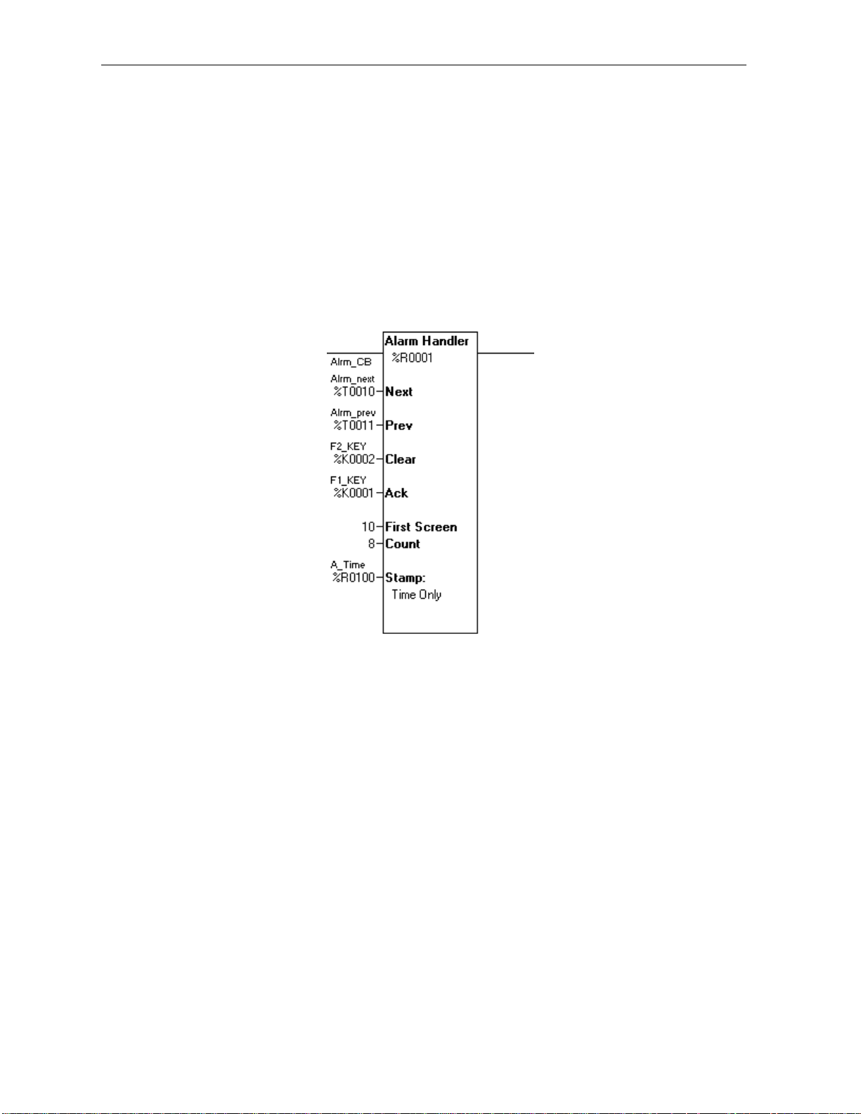
2.2.1 Overview
The alarm handling function block provides automatic display screen selection based on the current state
of one or more alarms. The alarm handling function block also acts as an alarm database controller in
that each alarm may be time stamped, counted, acknowledged, and cleared. Versatility is provided by
allowing the user to create a custom alarm screen for each defined alarm. This typically includes a userdefined message and information from the alarm database such as alarm status, alarm count and
time/date stamp information. Once a defined alarm occurs, its associated alarm screen is automatically
displayed. Once the displayed alarm is acknowledged and cleared (usually user intervention provided
though the OCS keypad), the previous display screen (or other pending alarms) is displayed.
Figure 2. 1 - Dialog Alarm Handing
Page 17
MAN0313-04 17 SEP 2002 PAGE 17
CH. 2
2.2.2 Alarm Status Registers - Alarm Control Block
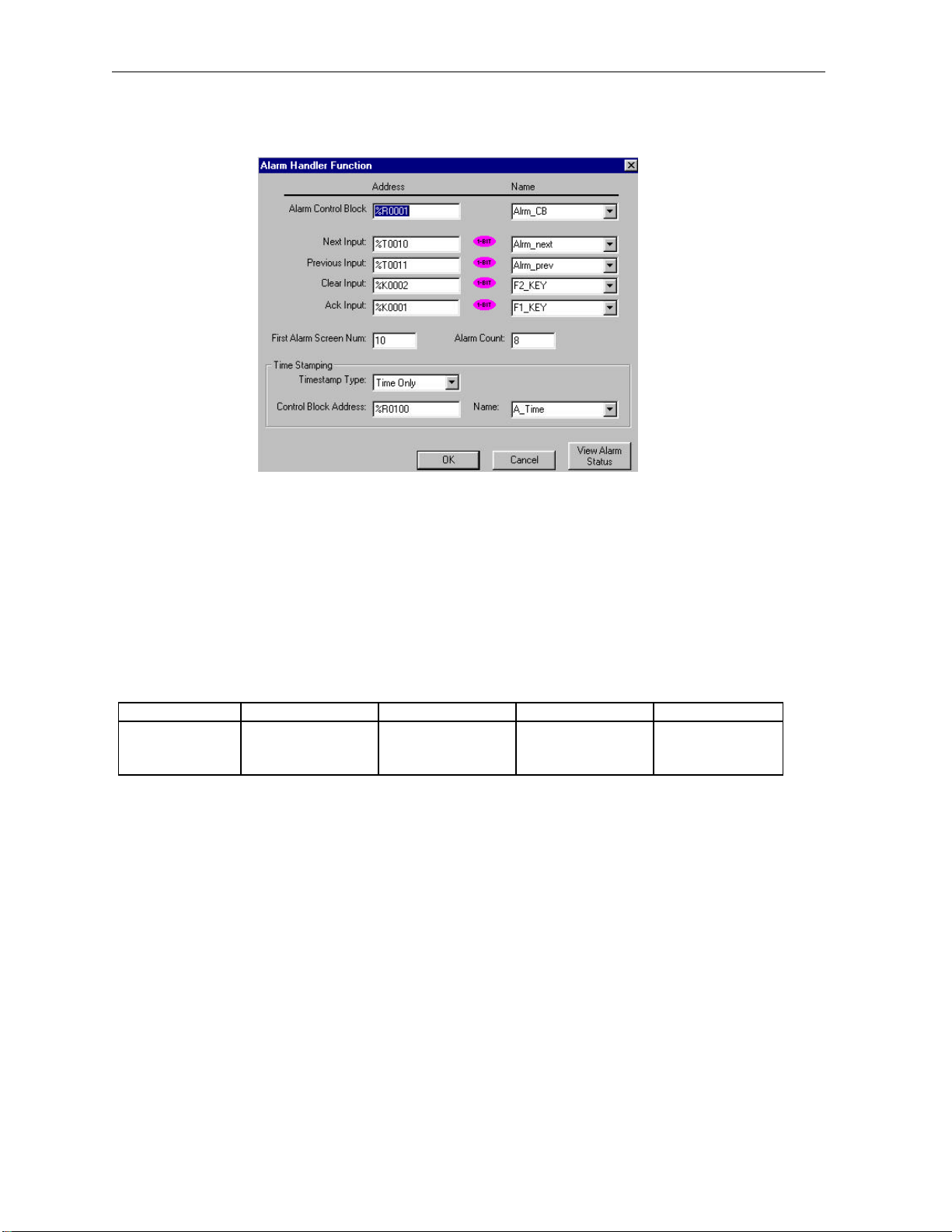
Figure 2.2 – Alarm Handler Function
Registers
Each alarm requires one 16-bit status register. The registers for multiple alarms are defined in a
contiguous block called the Alarm Control Block. One bit is written to this register to indicate that the
alarm is active. The register also contains sections that indicates the Acknowledge and Pending status
and contains a count for the alarm. By placing the alarm status registers in a section of retentive memory
(%R, %M...), the alarm states are retained through a power cycle.
The following table shows ho w the bits in the alarm status word (control block) are allocated:
16-12 11 10 9 8-1
Undefined
except for
Special Bits*
a. *Special Status Bits
§ Bit 16 of the fi rst status word turns ON when any alarm is pending. (The alarms may or may
not have been acknowledged.)
§ Bit 15 of the first status word turn ON when any alarm is unacknowledged.
b. Alarm Count - This is a BYTE counter that counts how many times an alarm occurs. The count
only increments when the pending bit goes from low to high. To count another alarm event the alarm
must be acknowledged, cleared and reactivated. When the count reaches a maximum of 255, it no
longer changes until reset. This count can be reset by writing directly to this portion of the register using
one of the BYTE instructions.
c. Active - This bit is set by the user's ladder program to indicate an alarm condition has occurred.
For example, if the alarm is to indicate an over-temperature condition, have the ladder logic perform a
compare function, and then, set this bit if the compare indicates the temperature is greater than a
setpoint.
Acknowledge Pending Active Alarm Count
Page 18

PAGE 18 17 SEP 2002 MAN0313-04
CH. 2
d. Pending - This bit is set by the function block when an alarm has occurred (active bit goes from
high to low), and the alarm has not been cleared.
e. Acknowledge - This bit is set by the function block after a pending alarm has been
acknowledged.
2.2.3 User Interface Settings
When alarms are displayed (one or more alarms pending and power flow enabled to the block), there are
four inputs that control the user interface to the function block. These inputs have no affect if there are no
pending alarms or if there is no power flow to the alarm handler function block.
a. Next - When this input transitions from low to high, the next (higher alarm number) pending alarm
is shown on the display. If the highest alarm is displayed, the alarm number is not incremented further.
b. Prev - When this input transitions from low to high, the previous (lower alarm number) pending
alarm is shown on the display. If the lowest alarm is displayed, the alarm number is not decremented
further.
c. Clear - When this input transitions from low to high, the currently displayed alarm is cleared if it
has already been acknowledged. If it has not been acknowledged, this input has no effect. Once an
alarm is cleared, an active bit turned ON in the status register causes the pending bit to be set, the alarm
count to increment and a time stamp (if enabled) to be recorded again.
d. Ack - When this input transitions from low to high, the currently displayed alarm is marked as
acknowledged. This sets the Acknowledge bit in the status register and allows the alarm to be cleared.
e. First Alarm Screen Num (First Screen) - Defines the first in a block of screens that are used to
display alarm information. Alarm 1 causes the screen defined by First Screen to be displayed, Alarm 2
causes the first screen plus one to be displayed.
f. Alarm Count (Count) - Sets the total number of alarms defined. This number also sets how
many registers are used for status registers, how many text screens are reserved for alarm display, and
how many registers are reserved for time stamping (if enabled).
2.2.4 Time Stamp Registers
Time stamping can be set to one of three modes:
a. None - No time stamping is performed and no additional register space is required.
b. Time Only - The time is recorded when each alarm's pending bit becomes active. Each alarm
requires three (3) registers starting at the block defined by the time-stamping control block. The time is
recorded in the same format as the real-time-clock is stored in the system registers.
c. Time and Date - The time and date is recorded when each alarm's pending bit becomes active.
Each alarm requires six (6) registers starting at the block defined by the time-stamping control block. The
time and date is recorded in the same format as the real-time-clock is stored in the system registers.
2.2.5 Power Flow
This function block only displays the pending alarms when power flow to the function block is ON. Alarm
screens are displayed by modifying %SR2 to force a screen based on the pending alarms and the NEXT
and PREV inputs.
Page 19
MAN0313-04 17 SEP 2002 PAGE 19
CH. 2
When power flow into the function block is OFF, the block continues to monitor the alarm active bits to
record alarm conditions including incrementing the alarm count, but it does not display the alarms.
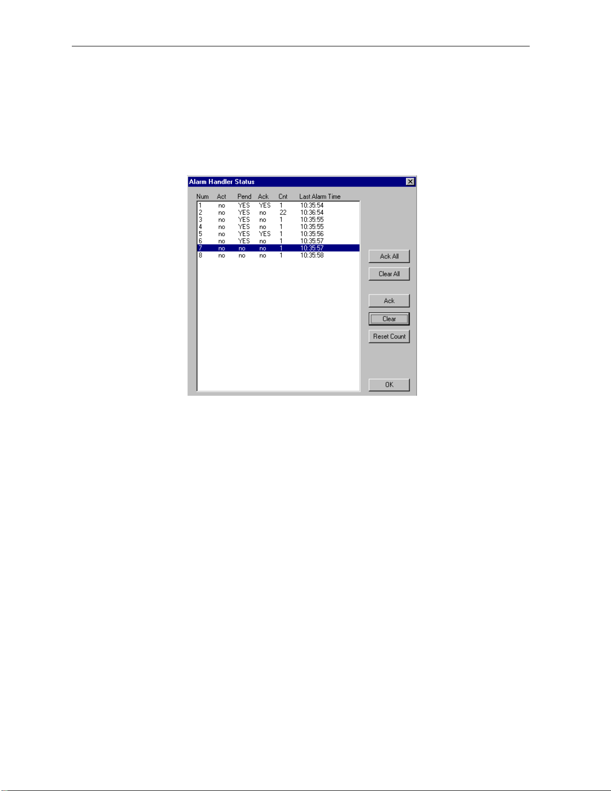
2.2.6 Viewing the Alarm Handler Status
From the alarm function block properties you can press the View Alarm Status button to view the
following dialog:
Figure 2. 3 - Alarm Handler Status
This dialog allows viewing real -time information for the alarms for the currently connect target controller.
Alarms can be acknowledged, cleared or the alarm counter can be cleared from this dialog.
Page 20

PAGE 20 17 SEP 2002 MAN0313-04
S N P
CH. 2
2.3 Boolean Elements
The following Boolean Elements are covered:
a. Normally Open Contact
Power is passed if the associated reference is ON.
b. Normally Closed Contact
Power is passed if the associated reference is OFF.
c. Normally Open Coil
The associated reference is set ON if the coil receives power.
d. Normally Closed Coil
The associated reference is set OFF if the coil receives power.
e. Positive Transition Coil
If the associated discrete reference is OFF when the coil receives power, the reference is set ON for one
logic scan.
f. Negative Transition Coil
If the associated discrete reference is ON and the coil is not receiving power, the reference is set ON for
one logic scan.
g. Set Coil
The associated discrete reference is set ON if coil receives power. It remains set until it is reset by
a Reset Coil.
Page 21

MAN0313-04 17 SEP 2002 PAGE 21
R
CH. 2
h. Reset Coil
The associated discrete reference is set OFF if coil receives power. It remains set until it is set by
a Set Coil.
2.4 Display Elements
2.4.1 How to Use Display Screens
Cscape supports the OCS product lines built-in screens.
When a coil is used with a %D register it becomes a screen display coil. This allows ladder to easily
control the screen number being shown on the display. When a coil is used as a screen display coil there
are two options force screen and switch screen.
Force Screen - This displays a screen as long as the coil is active. This will override any other user
screen being displayed. If more than one force screen is active at one time, the one that appears last in
the ladder program is the one that is displayed. When a screen is being forced, its screen number can be
read from %SR2, the alarm screen number.
Switch Screen - This allows the ladder program to switch the operator to a screen, but does not force
this screen to remain active. The operator may choose to switch screen after the screen switch using
various navigation methods(menus, screen jumps, scrolling...). Only one switch screen coil should be
active at one time. If a switch screen is active and another one becomes active it will have no affect,
however writing to %SR1 will change the screen while the switch screen is active.
NOTE: Power does not flow through the display coil. [See Next]
2.4.2 How to Create a Display Coil
To create a display screen start with a coil:
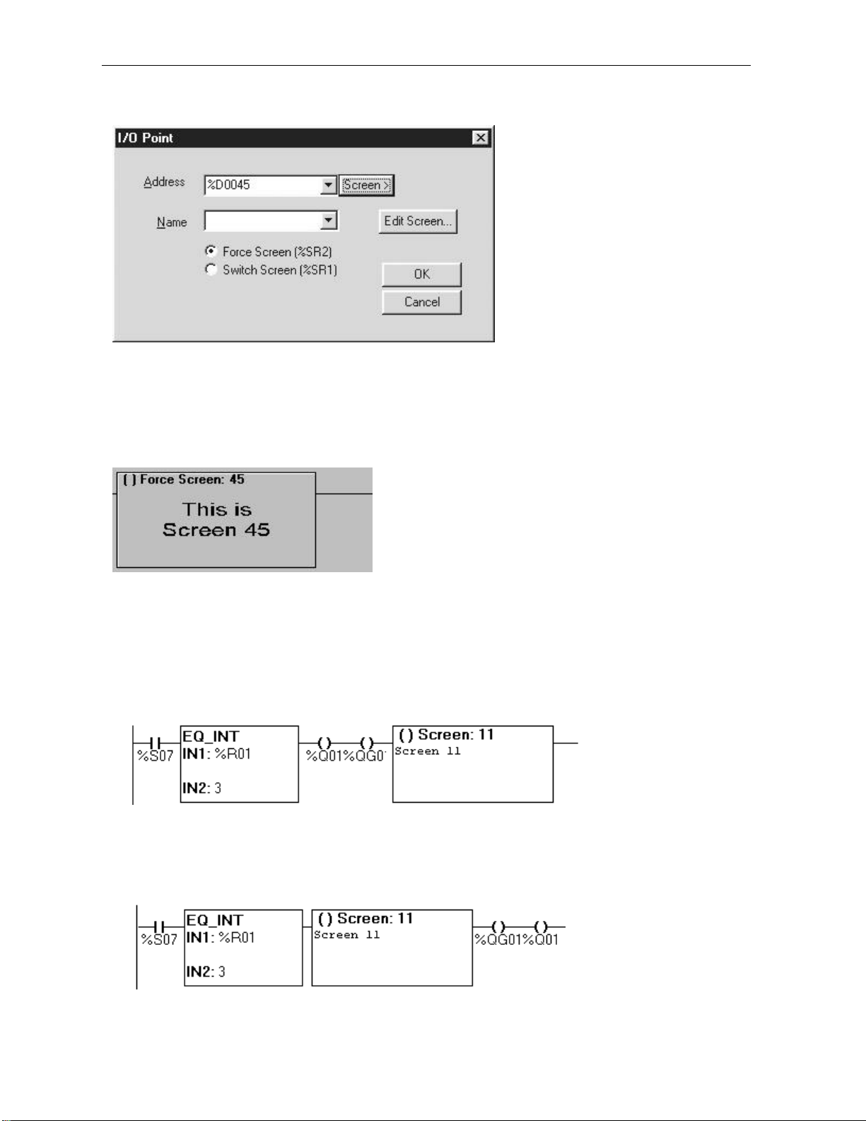
Enter %D, then the screen number or press the "Screen >" button to see the screen picker.
Page 22
PAGE 22 17 SEP 2002 MAN0313-04
CH. 2
Figure 2.4
Decide if you want a force screen or switch screen, then press OK.
The coil now expands to show a thumbnail of the screen if available.
Figure 2.5
Power Flow through the Element
Power does not flow through the Display Screen coil. The Display Screen Coil must be the last (rightmost) element on the rung. In order to activate multiple output coils on the same rung, the Display coil
%D must be the last coil on the rung.
Acceptable
Not Acceptable
Page 23

MAN0313-04 17 SEP 2002 PAGE 23
CH. 2
Using Screen Number System Registers
See Also: System Registers
The controllers contain system registers that allow the user, alarm and system screen numbers to be read
and/or written.
The following is a definition of the three types of screens:
System Screens -
These are the predefined screens that make-up the system menu. System screen one is viewed by
pressing the system key on the controller. Additional system screens can be viewed by navigating the
various menus that make-up the system menu. Any system screen can also be displayed by writing a
screen number to the system screen system register. System screens are shown even if alarm or user
screens are active.
Alarm Screen These screens are programmer defined screens that are forced to display using a %D coil in ladder logic.
The alarm screen system register can be read to determine which screen is being forced as an alarm.
Writing to the alarm screen system register does not affect operations bec ause the ladder processor
calculates and writes the alarm screen number each scan. These screens can be marked as Alarm
when creating the screens, but screens that are not marked as Alarm, but are forced using %D coils are
considered alarm screens in this context.
User Screen -
If a system screen and alarm screen is not displayed, a user screen is displayed. The If more than one
user screen exist (programmer not defined as Alarm), the operator can switch between screens using the
UP and DOWN keys on the controller. Reading the user screen system register allows the ladder
program to monitor the operators movement through the screens as they scroll using the UP and DOWN
keys. Writing to the user screen system register allows the ladder program to directly control the screen
being displayed.
Page 24
PAGE 24 17 SEP 2002 MAN0313-04
CH. 2
2.4.3 Multiple Active Screens
If more than one screen is activated during any one program scan, the last processed screen is
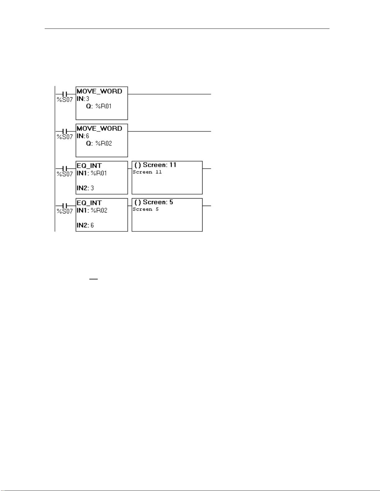
displayed. This happens in the following code:
MULTIPLE ACTIVE SCREENS
In this case, both Screen 11 and Screen 5 are active, but Screen 5 is displayed, because it is the last
screen processed in the scan of this logic.
This situation is not wrong logically or syntactically, so no errors are reported during compile or run. It is
the programmer's responsibility to determine if this situation is acceptable or provide corrective action if
necessary.
2.5 Logic (Bitwise) Operator Elements
2.5.1 General
NOTE: Bitwise Elements (AND, OR, etc.) operate on WORDS (string of 16 bits) or DWORDS (string of 32
bits).
When using constants with Bitwise elements, enter them as 16 or 32 -bit UNSIGNED values. Operations
are performed on the bit patterns of the register. After the operation, the results are stored in a third result
register. Neither input is changed.
2.5.2 Power Flow Through the Element
These elements are always TRUE. Power always passes though these elements without dependency on
the output value.
Page 25
MAN0313-04 17 SEP 2002 PAGE 25
CH. 2
2.5.3 Configuring Logic Elements
To configure the element, double click it, and then enter the Register Type and Offset (address) for both
input registers and the output register. Three (3) registers are required for proper operation of these
elements: IN1, IN2, and Q (result) except the NOT function, which requires only one input and one output
register.
Either input can be an unsigned WORD or DWORD constant, 1, 23056, 45, etc. In fact, both inputs can
be constants
The Q (result) register must be specified using Register Type and Offset
These functions can operate on either 16-bit integer values or 32-bit value. From the Type drop-down list,
select either Word (16-bit) or DWord (32-bit). Both values must be of the same data type, WORD or
DWORD.
NOTE: It is not possible to use both a 16 -bit register and a 32-bit register in the same element..
In most cases these elements operate on registers capable of holding Word or Dword values such as %R
or %AI. It is possible, however, to use discrete (Boolean points by specifying a Register Type and Offset
such as %Q17. The Offset used must be on a 16 -bit boundary 1, 17, 33, etc.
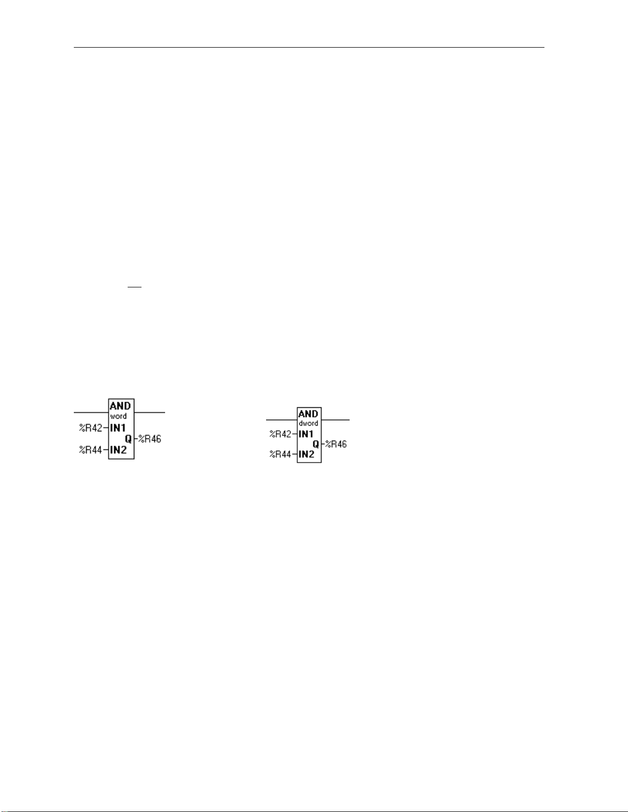
AND
This element performs a bit-wise AND on two registers and places the output in a third.
BITWISE AND BITWISE AND DWORD
For example,
%R41 = 0000000000000111 ( 7 )
AND %R42 = 0000000000001010 (10 )
RESULT %R43 = 0000000000000010 ( 2 )
Page 26
PAGE 26 17 SEP 2002 MAN0313-04
CH. 2
OR
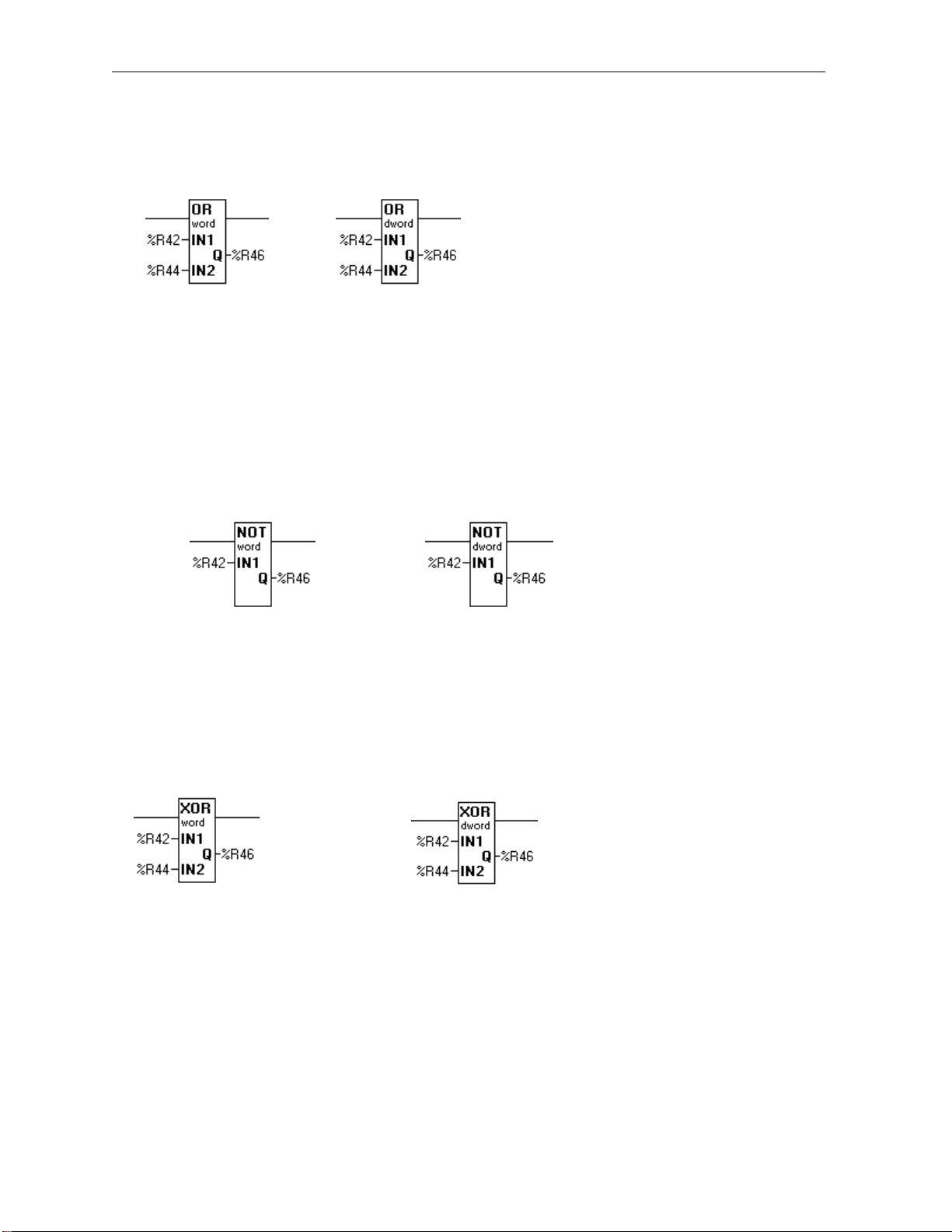
This element performs a bit-wise OR between two registers, and places the output in a third.
BITWISE OR OR DWORD
%R41 = 0000000000000111 ( 7)
OR %R42 = 0000000000001010 (10)
RESULT %R43 = 0000000000001111 (15)
NOT
This element performs a bit-wise NOT on a single register and places the output in a second register.
BITWISE NOT NOT DWORD
%R41 = 0000000000001010 (10)
NOT %R43 = 1111111111110101 (65525 (unsigned) or -11(signed))
EXCLUSIVE OR
This element performs a bit-wise EXCLUSIVE OR between two registers and places the output in a third.
BITWISE XOR XOR DWORD
%R41 = 0000000011111111 (255)
XOR %R42 = 0000000010100101 (165)
RESULT %R43 = 0000000001011010 (90)
Page 27
MAN0313-04 17 SEP 2002 PAGE 27
CH. 2
2.6 Math Operations
NOTE: The Math Operations work on INT (16 -bit) or DINT (32 -bit) SIGNED integer values and REAL
(floating-point) values.
2.6.1 Performance
INT (16 -bit) and DINT (32-bit) operations are very close to each other in performance and can be used
interchangeably without noticeably affecting the OCS's performance.
REAL (floating point) operations always take more time to execute and can be significantly slower than
the INT or DINT counter part. Try to keep values in INT or DINT format whenever possible and for as
long as possible.
For example, temperatures are often measured using a thermocouple, whose values are converted to
binary form by a Thermocouple Interface SmartStack module. The value obtained from the Thermocouple
Interface module is always in INT (16 -bit) format, even though it represents a fractional number of
degrees. The first thought is to convert the binary value to its Real va lue (degrees and fractions of
degree). However, it is more likely that any necessary mathematical operations can be written to use this
raw value (saving any conversion to a Real value) (if and when the value is displayed to the user).
Power flow through these elements is ON or TRUE if the element completes properly. Power Flow is OFF
or FALSE if an error occurs such as overflow, underflow, divide by zero.
2.6.2 Configuring Math Operation Elements
To configu re the element, double click it, and then enter the Register Type and Offset (address) for both
input registers and the output register. Three (3) registers are required for proper operation of these Math
Elements. Either IN1 or IN2 or both can be signed constants. Q must be a register reference.
In the Type box select either INT (16-bit), DINT (32-bit) or REAL (32-bit) operations. For INT operation,
only single 16-bit registers (%R43, %AI02, etc) are affected. For DINT (32-bit) and REAL (32-bit)
operations, registers are accessed in 32-bit pairs, %R43 and %R44, etc.
NOTE: Both inputs and the output must be of the same type, INT, DINT, or REAL.
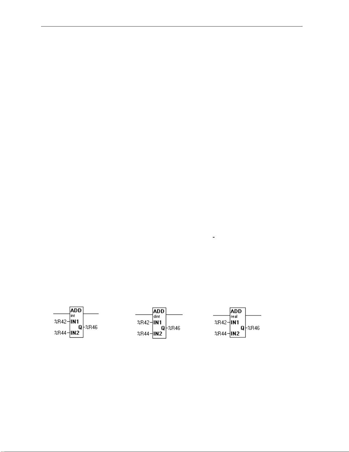
2.6.3 Math Operations
ADD
INTEGER ADD DINT ADD REAL ADD
This element adds IN1 and IN2, and places the result in Q.
Q = IN1 + IN2
Page 28
PAGE 28 17 SEP 2002 MAN0313-04
CH. 2
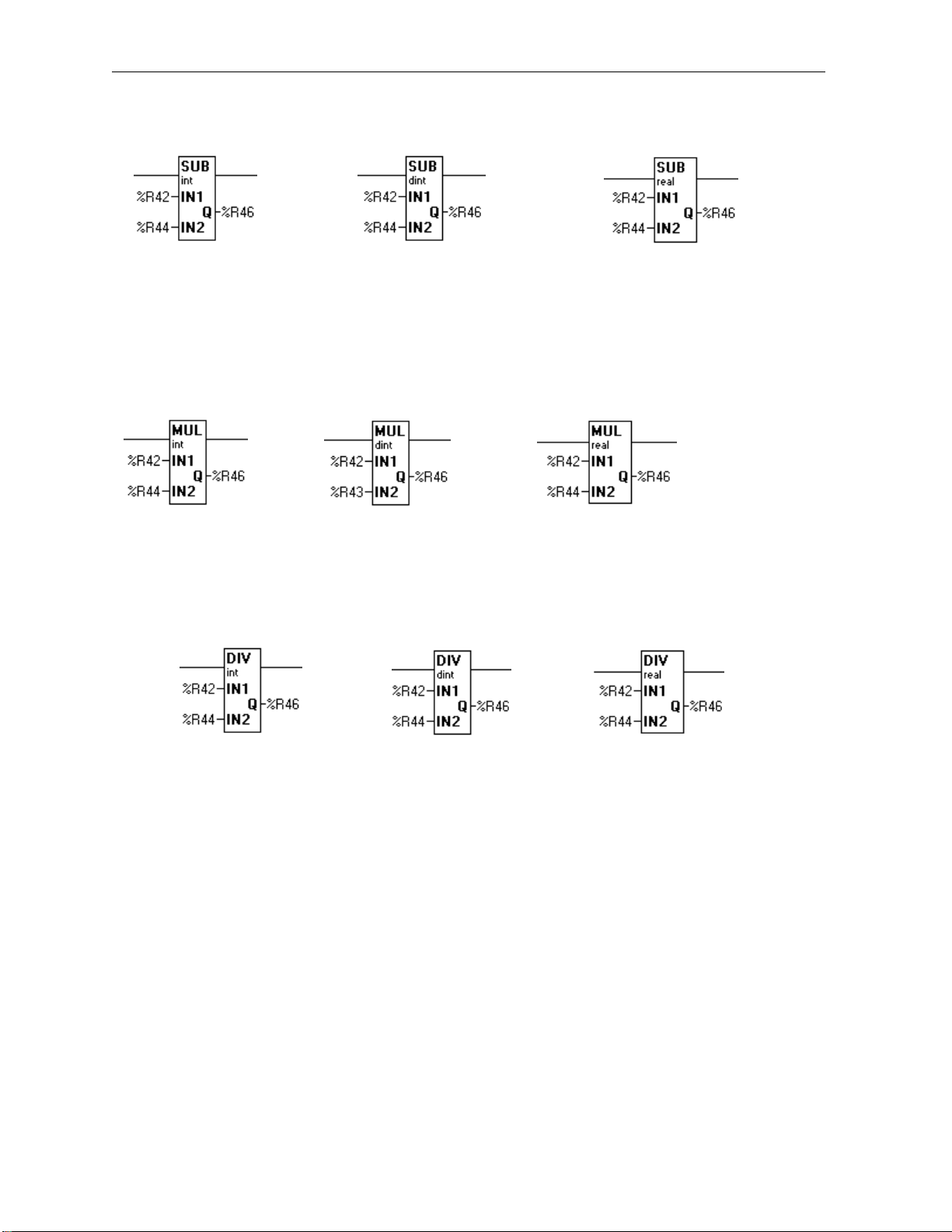
Subtract
INTEGER DINT REAL
SUBTRACT SUBTRACT SUBTRACT
This element subtracts IN2 from IN1 and places the results in Q.
Q = IN1 - IN2
Multiply
INTEGER MULTIPLY DINT MULTIPLY REAL MULTIPLY
This element multiples IN1 and IN2 and places the results in Q.
Q = IN1 * IN2
Divide
ELEMENT INTEGER DIVIDE ELEMENT DINT DIVIDE ELEMENT REAL DIVIDE
This element divides IN1 by IN2 and places the result in Q.
Q = IN1 / IN2
Page 29
MAN0313-04 17 SEP 2002 PAGE 29
CH. 2
If the values are INT or DINT, any remainder is lost. For example, given the IN2 value of 5, the following
is a table of some Integer Divide values:
IN1 IN2 Q
10 5 2
11 5 2
12 5 2
13 5 2
14 5 2
15 5 3
16 5 3
17 5 3
18 5 3
19 5 3
20 5 4
21 5 4
22 5 4
23 5 4
24 5 4
25 5 5
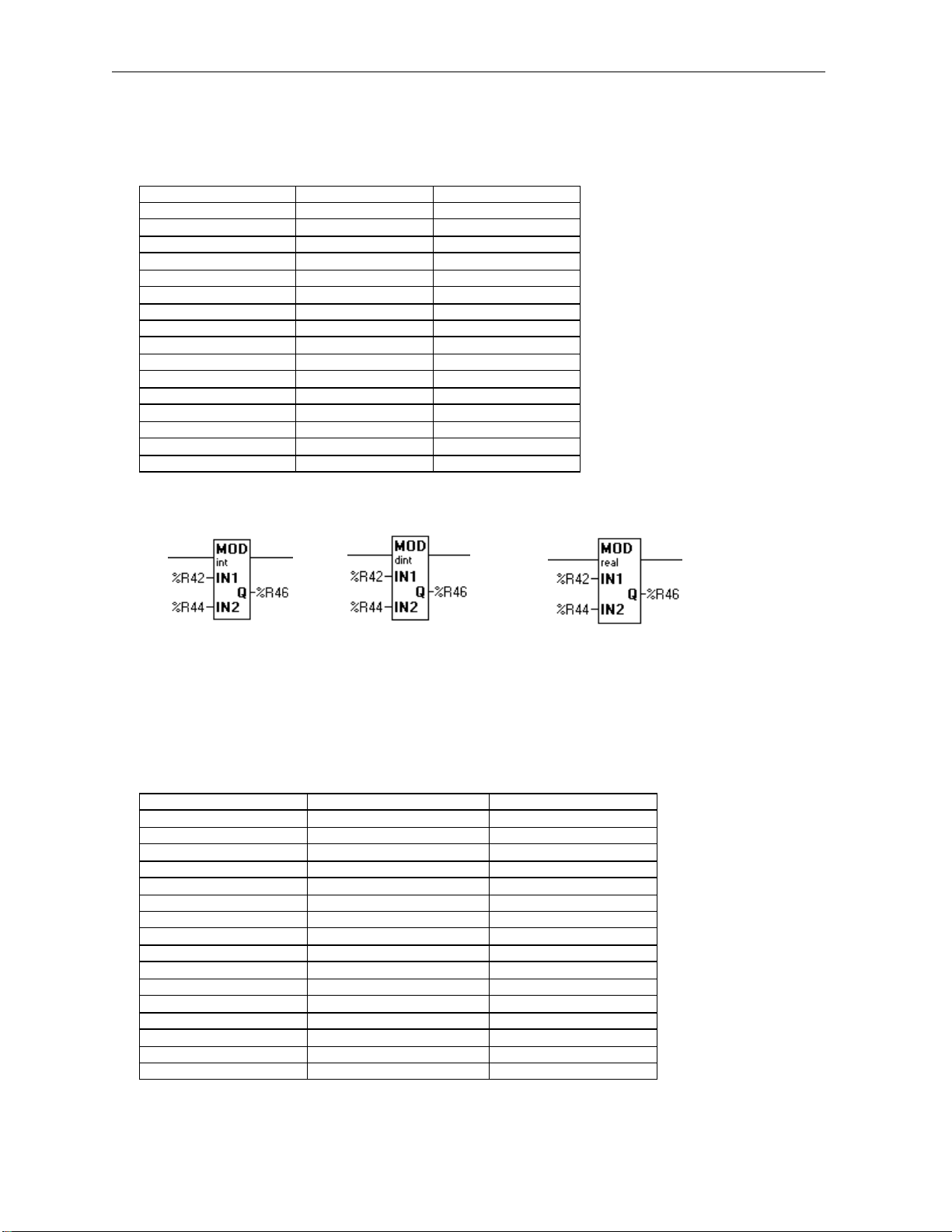
MOD (modulo)
INTEGER MOD ELEMENT DINT MOD ELEMENT REAL MODULO
This element divides IN1 by IN2 (the modulus) and places the remainder in Q.
Q = remainder(IN1 / IN2)
For example, given the IN2 value of 5, the following is a table of some modulo values:
IN1 IN2 Q
0 5 0
1 5 1
2 5 2
3 5 3
4 5 4
5 5 0
6 5 1
7 5 2
8 5 3
9 5 4
10 5 0
11 5 1
12 5 2
13 5 3
14 5 4
15 5 0
Page 30
PAGE 30 17 SEP 2002 MAN0313-04
1
3.12
1.02
2.1
2.1
CH. 2
Performing the Modulo function on Real Numbers can appear to behave strangely if the internal workings
are not understood. For example, 3.12 MOD 2.1 = 1.02. This can be better illustrated using long
division:
Integer Result
Modulo
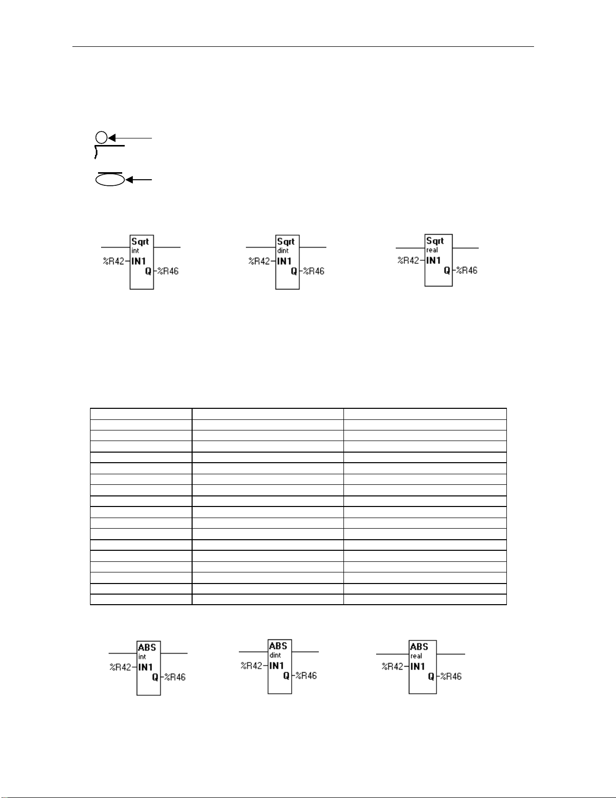
Square Root
INTEGER SQRT DINT SQRT REAL SQUARE ROOT
This element figures the square root of the value in IN1 and places the result in Q.
Q = SQR(IN1)
This element has its primary use with REAL data types. This element does work with INT (16 -bit) or DINT
(32-bit) data, but the results of the square root function are seldom integers. The result placed in Q is
truncated to the integer value.
IN1 Actual Q
0 0 0
1 1.000 1
2 1.414 1
3 1.73 1
4 2.000 2
5 2.236 2
6 2.449 2
7 2.645 2
8 2.828 2
9 3.000 3
10 3.162 3
11 3.316 3
12 3.464 3
13 3.605 3
14 3.741 3
15 3.872 3
16 4.000 4
Absolute Value
ABS DINT ABS REAL ABS
Page 31
MAN0313-04 17 SEP 2002 PAGE 31
CH. 2
This element takes the value of IN1 strips off the sign, and places the results in Q.
Q = ABS(IN1)
The result is always positive.
2.6.4 Advanced Math Operations
NOTE: The Advanced Math functions operate on REAL (floating point) numbers only.
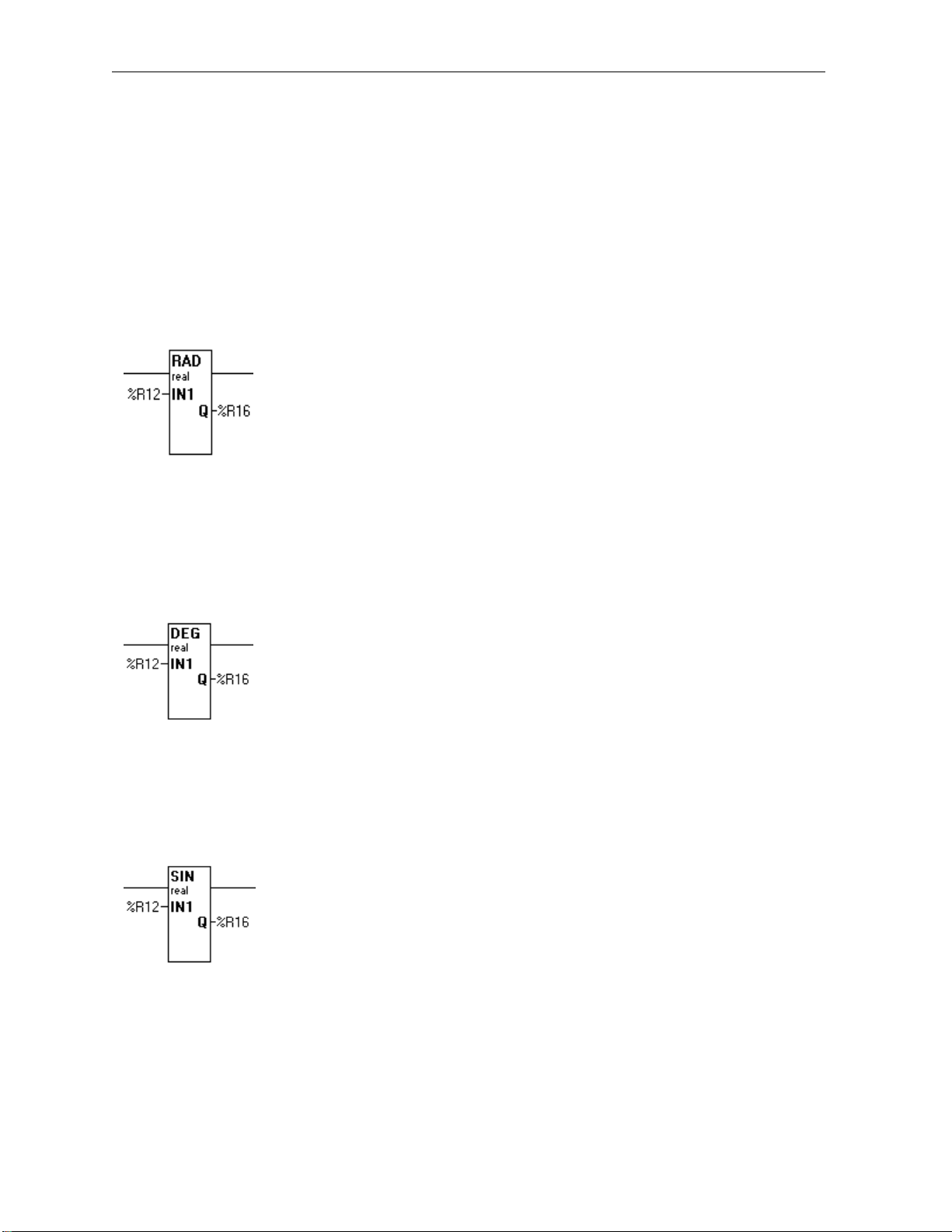
Radians
RADIANS
The value IN1 is converted from DEGREES to RADIANS, and the result placed into Q. IN1 is expressed
in DEGREES. Q is expressed in RADIANS.
Q = RAD(IN1)
Degrees
DEGREES
The value IN1 is converted from RADIANS to DEGREES, and the result placed into Q. Input values are
expressed in RADIANS. Output values are expressed in DEGREES.
Q = DEG(IN1)
Sine
SINE
The SINE of the value IN1 is placed into Q. Values in IN1 are expressed in RADIANS. Output values
range from -1 to +1.
Q = SIN(IN1)
Page 32
PAGE 32 17 SEP 2002 MAN0313-04
CH. 2
Cosine
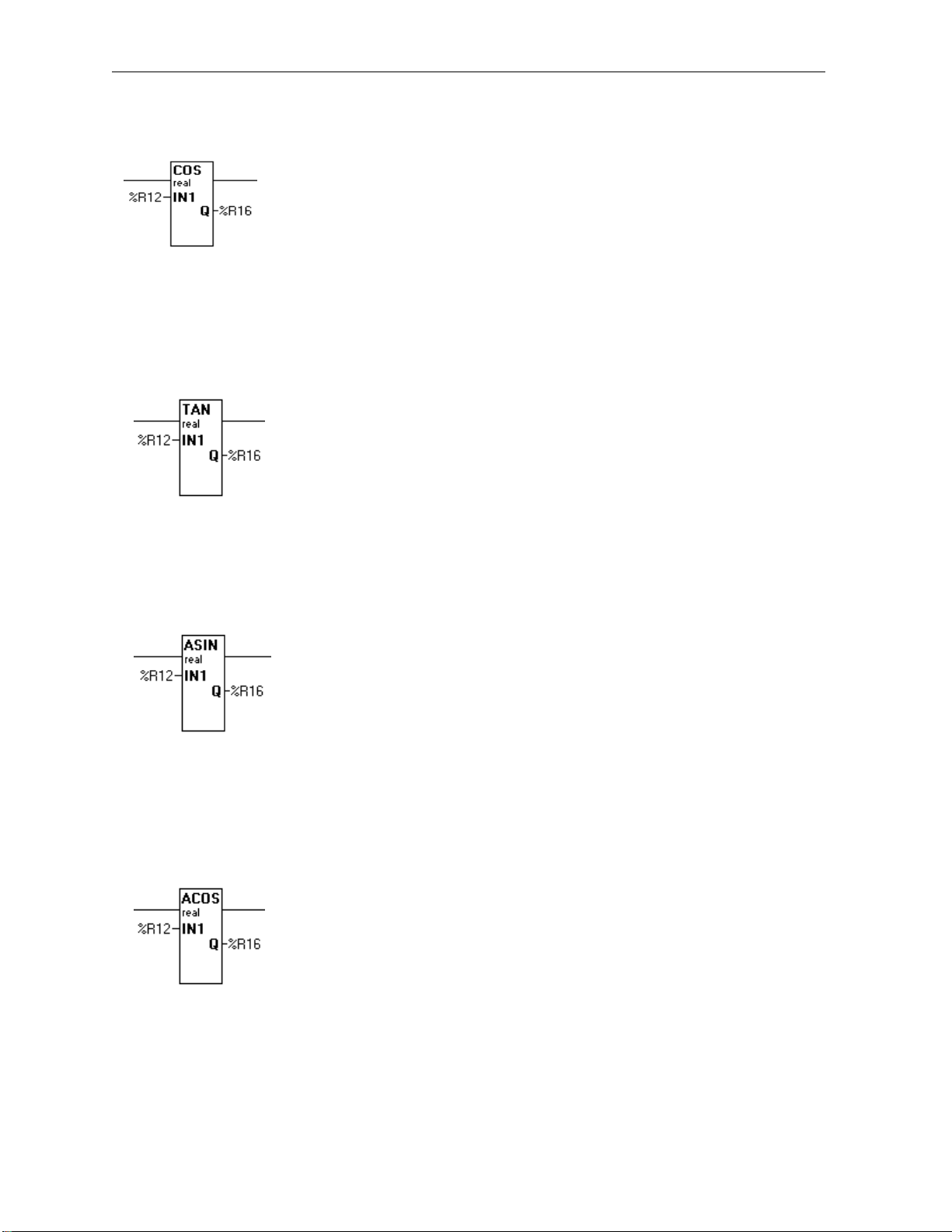
COSINE
The COSINE of the value IN1 is placed into Q. Values in IN1 are expressed in RADIANS. Output values
range from -1 to +1.
Q = COSIN(IN1)
Tangent
TANGENT
The TANGENT of the value IN1 is placed into Q. Values in IN1 are expressed in RADIANS.
Q = TAN(IN1)
Arc Sine
ARC SINE
The ARC SINE of the value IN1 is placed into Q. Input values must be in the range -1 to +1. Output
values are expressed in RADIANS.
Q = ASIN(IN1)
Arc Cosine
ARC COSINE
The ARC COSINE of the value IN1 is placed into Q. Input values must be in the range -1 to +1. Output
values are expressed in RADIANS.
Q = ACOSIN(IN1)
Page 33
MAN0313-04 17 SEP 2002 PAGE 33
CH. 2
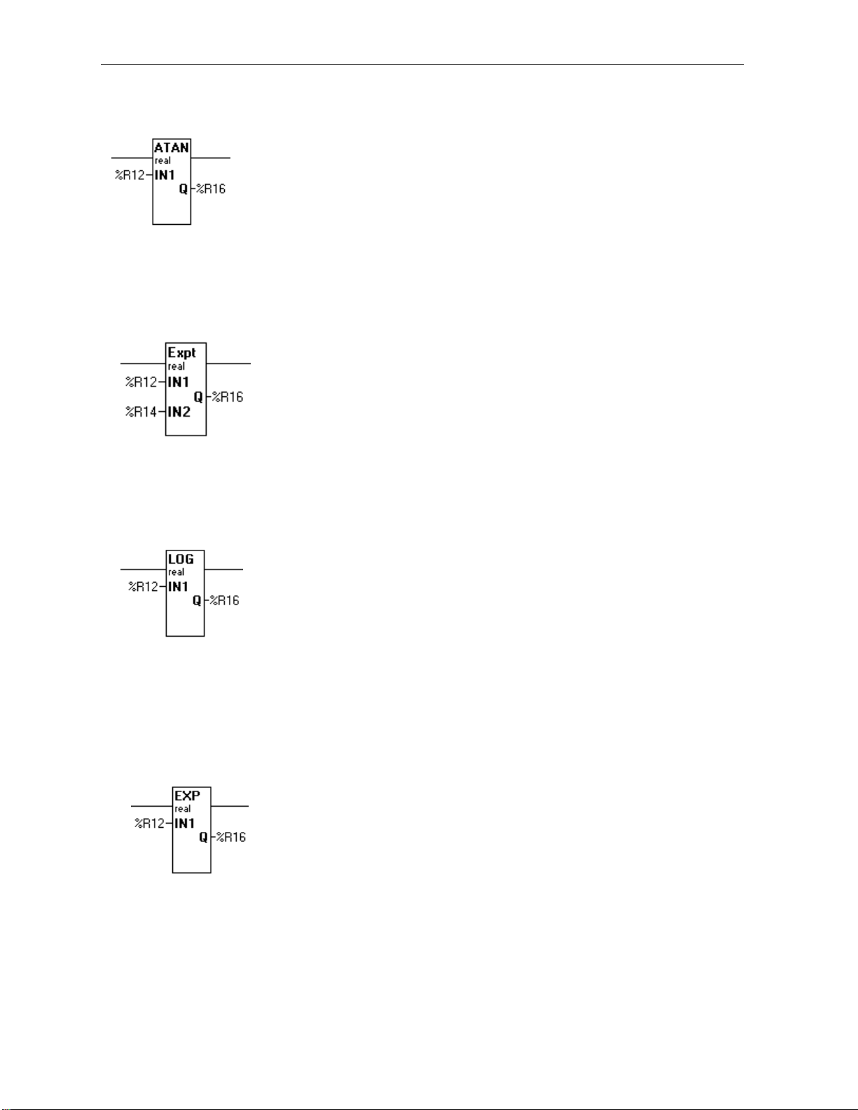
Arc Tangent
ARC TANGENT
The ARC TANGENT of the value IN1 is placed into Q. Output values are expres sed in RADIANS.
Q = ATAN(IN1)
Exponentiate
EXPONENTIATE
This function raises IN1 to the IN2 power and places the result in Q.
Q = IN1
IN2
Common Logarithm
ELEMENT LOG.
This function determines the common (base 10) logarithm of IN1 and places that value into Q.
Q = LOG(IN1)
Exponent
EXPONENT
This function determines the value of e (the base of natural logarithms) raised to the IN1 power and
places the result in Q.
IN1
Q = e
Page 34
PAGE 34 17 SEP 2002 MAN0313-04
CH. 2
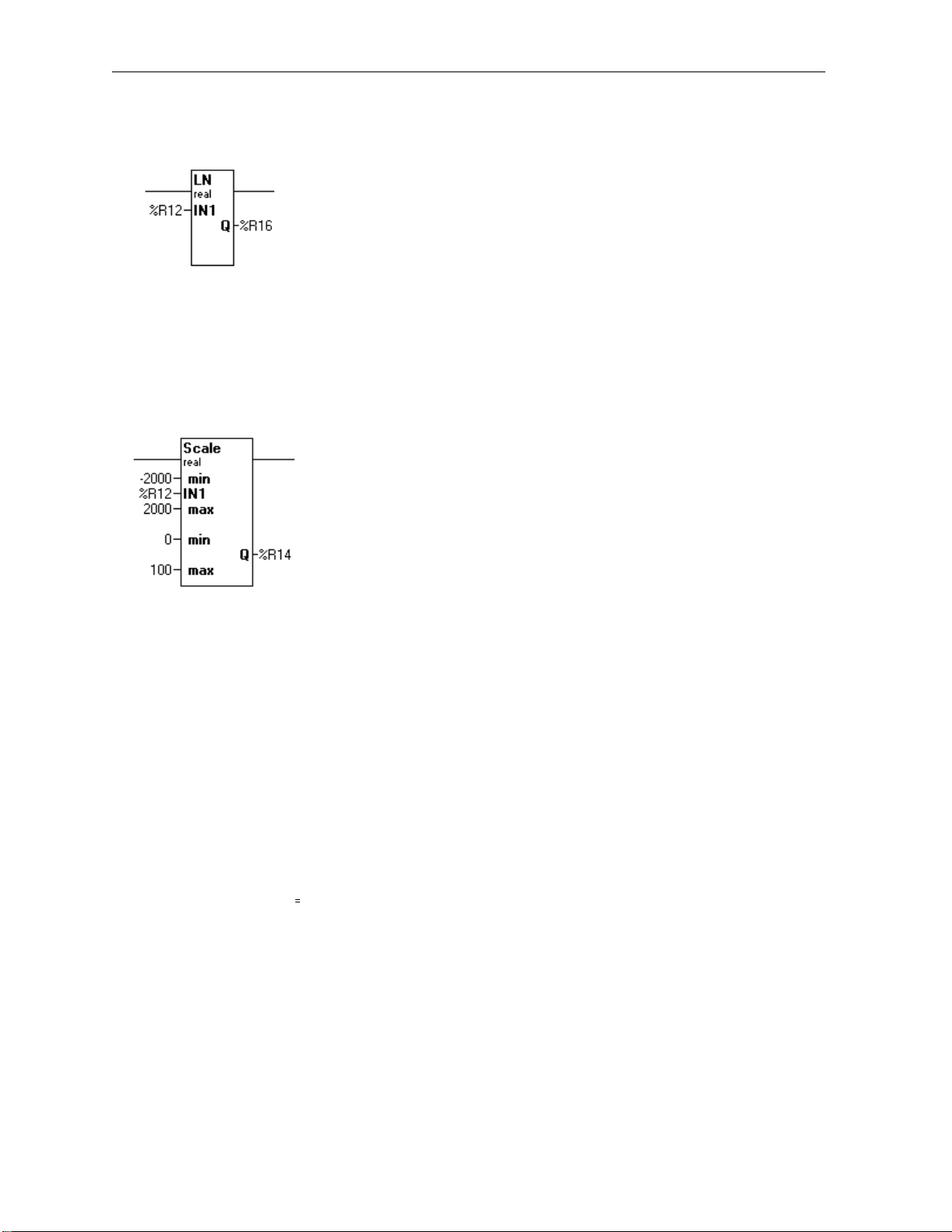
Natural Logarithm
ELEMENT LN
This function determines the natural log of IN1 and places the result in Q.
Q = LN(IN1)
Scaling
SCALING
Note: Scaling works only with INT and Floating Point (real) numbers. If Double Integer values are used it
is necessary to convert inputs to Real format before scaling and possibly convert the scaled value
back to Double Integer.
Cases often a rise when numbers on one scale need to be translated to another scale. For example, the
raw output of a level transmitter needs to be converted into a 0-to-100-percent scale. Doing so is called
scaling.
In the Scaling Element configuration dialog, select a Register Type and Offset reference or select a
Named Variable that is the raw Input Value.
The Minimum and Maximum Ranges indicted the expected or nominal values that the Input can be
expected to attain. This is the range of values that corresponds to the expected output range.
Select Register Type and reference or select a Named Variable that is the Output Value.
The Minimum and Maximum Ranges indicate the range of value that the Input signal is converted to.
Page 35
MAN0313-04 17 SEP 2002 PAGE 35
CH. 2
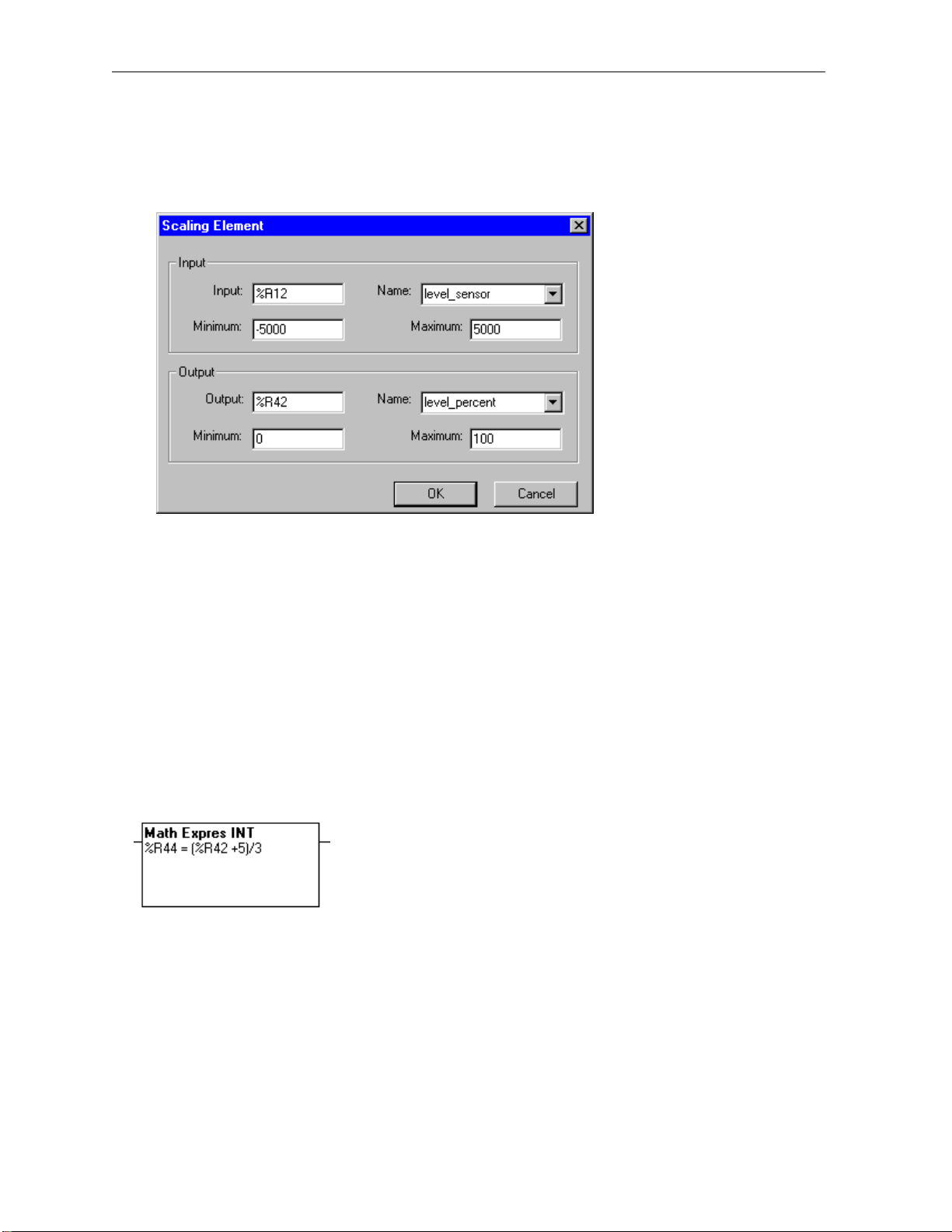
For example, suppose that one is monitoring the fill level of a tank of liquid. This device sends back raw
data that ranges from -5000 (empty) to +5000 (full). The values are to be converted to a range of 0 (zero)
to 100 percent. Configure the element thus:
EXAMPLE SCALING ELEMENT
2.7 Math Equation Element
NOTE: The Math Equation element operates on 16-bit SIGNED Integers 32-bit SIGNED integers or 32 -bit
REAL numbers
2.7.1 Useful Math Feat ure of Cscape
Cscape contains a feature to allow potentially complicated math operations to be expressed in standard
mathematical notation and then be performed in a single program element. This can reduce or eliminate
many program rungs which makes the resulting program simpler to write and easier to understand.
MATH EXPRESSION
2.7.2 Power Flow Through the Element
Power flow through the element is ON or TRUE if the equation is solved successfully. If any math error
occurs (e.g., divide by zero), the power flow through the element is OFF or FALSE.
If any math error occurs, the value placed into the left side of the equation is invalid.
Page 36
PAGE 36 17 SEP 2002 MAN0313-04
CH. 2
2.7.3 Configuring Math Equations
To configure a math equation, double click on the element, and then type in the desired equation in the
format:
[result] = [equation]
[result] must be a register, typically %R.
= is a REQUIRED equal sign.
[equation] is the equation to be performed.
The TOTAL length of the equation string is limited to 80 characters. This includes the result location
specification and equal sign (%R5 = ) and the equation itself.
The complete equation can be configured to use either INT (16-bit), DINT (32-bit) or REAL values. Note
that all references in the equation are of the type selected.
NOTE: It is not possible to mix INT (16 -bit), DINT (32-bit) or REAL values in the same equation.
NOTE: Multiplication must be explicitly shown. %R4 = 4(%R1 + 4) is NOT valid. It must be expressed
as %R4 = 4 * (%R1 + 4).
2.7.4 Typing Shortcut
In order to save typing time and to reduce the possibilities of typing errors, available operations are
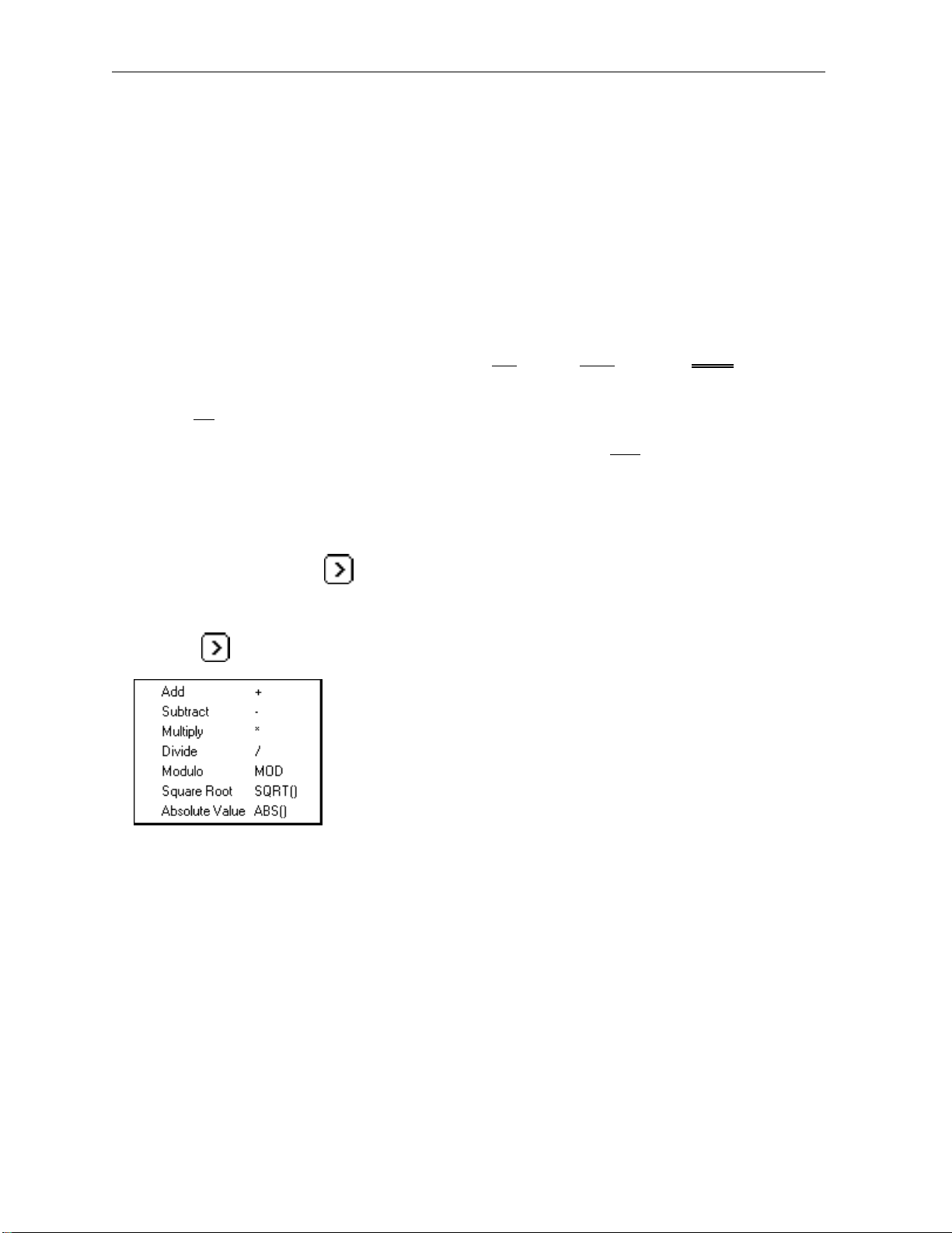
selected from the More menu .
First, place the cursor in the equation at the point where an operation is to appear, and then click the
More button . A pop up menu appears:
MENU MORE POPUP
After the operation is inserted, move the cursor into position to edit the operation, if necessary.
Page 37

MAN0313-04 17 SEP 2002 PAGE 37
Warning: If INT or DINT math is performed, this equation may not produce the
CH. 2
2.7.5 Register Designation
The result of the equation must be placed in a register. Typically, this is a %R, although other registers
(%AQ...) can be used. The size of the register, 16- or 32 -bits, is determined by the setting of the Type
box. 16- or 32 -bit groups of Boolean registers (e.g., referencing %Q17, thus specifying register %Q17 %Q32) can also be used.
The register can be specified using either its predefined name or the type and offset of the register:
Temp_Result = [equation]
%R10 = [equation]
NOTE: Since Names are valid, Register Types must be preceded with % (percent sign) in order for them
to be properly recognized as register references.
2.7.6 Numeric Constants
Numeric constants may be used by simply entering them:
(* This element converts readings
from Centigrade to Fahrenheit *)
%R22 = (%R15 * (9/5)) + 32
expected results.
2.7.7 Operators
Equations are entered in standard mathematical format. The expected orders of precedence are used:
ABS() Highest
SQRT()
LOG()
EXP()
LN()
SIN()
COS()
TAN()
ASIN()
ACOS()
ATAN()
DEG()
RAD()
EXPT
* (multiply)
/ (divide)
MOD
+ (add)
- (subtract)
= Lowest
Page 38

PAGE 38 17 SEP 2002 MAN0313-04
CH. 2
Operational order can be changed by using parenthesis ( ). Nested parenthesis ( ( ) ) may be as deep
as necessary , provided the 80 character limit of the equation string is not exceeded.
For example, the following math equation is valid:
%R22 = (%R15 * %R16) + (%R15 / %R16)
If %R15 contains 25 and %R16 contains 5, then %R22 contains 130 after the element is complet ed.
2.8 Compare Elements
NOTE: Compare Elements (EQ_INT, etc.) operate on unsigned BYTE (8-bit) values 0 to +255, Signed
Integer (16-bit) values, -32768 to +32767,Signed Double Integer (32-bit) values, -2147483648 to
+2147483647, or Floating Point values, +/-3.40282e-38 to +/-3.40282e+38.
2.8.1 General
Compare Elements take the values of two BYTE (8-bit), Integer (16-bit) SIGNED values, Double Integer
(32-bit) SIGNED values or Floating Point (32 -bit) values and performs a comparison on the two values in
the form IN1[comparison]IN2, such as IN1<IN2.
2.8.2 Power Flow Through the Element
When the comparison is TRUE, power is passed through the element to its output, which can be used to
set or clear an indicator coil. For example:
Given: Comparison Power Flower
IN1 = 6 IN2 = 3 IN1 > IN2 TRUE
IN1 = 6 IN2 = 3 IN1 < IN2 FALSE
IN1 = 6 IN2 = 3 IN1 = IN2 FALSE
IN1 = 3 IN2 = 6 IN1 > IN2 FALSE
IN1 = 3 IN2 = 6 IN1 < IN2 TRUE
IN1 = 3 IN2 = 6 IN1 = IN2 FALSE
2.8.3 Configuring Compare Element
To configure the element, double click it, and then enter the Register Type and (address) for both inputs.
Either input can be a BYTE integer, double integer or real constant, (1,23056, 4.23e+5 etc). In fact, both
inputs can be constants, but the result of the comparison would is a fixed TRUE or FALSE.
From the Type drop-down list select either BYTE (8-bit) INT (16 -bit) or DINT (32-bit). Both values and
the result must be of the same data type, BYTE, Integer, Double Integer, or Real.
NOTE: It is not possible to mix register types; 16 -bit integer, 32-bit double integer, or 32-bit floating-point
(real).
In most cases, these elements operate on registers capable of holding INT or DINT values such as %R or
%AI. It is possible, however, to use discrete Boolean points by specifying a Register Type and Offset
such as %Q17. The Offset used must be on a 16 -bit boundary (1, 17, 33, etc). When the configuration is
complete, the element indicates whether INT, DINT or values are used.
Page 39
MAN0313-04 17 SEP 2002 PAGE 39
CH. 2
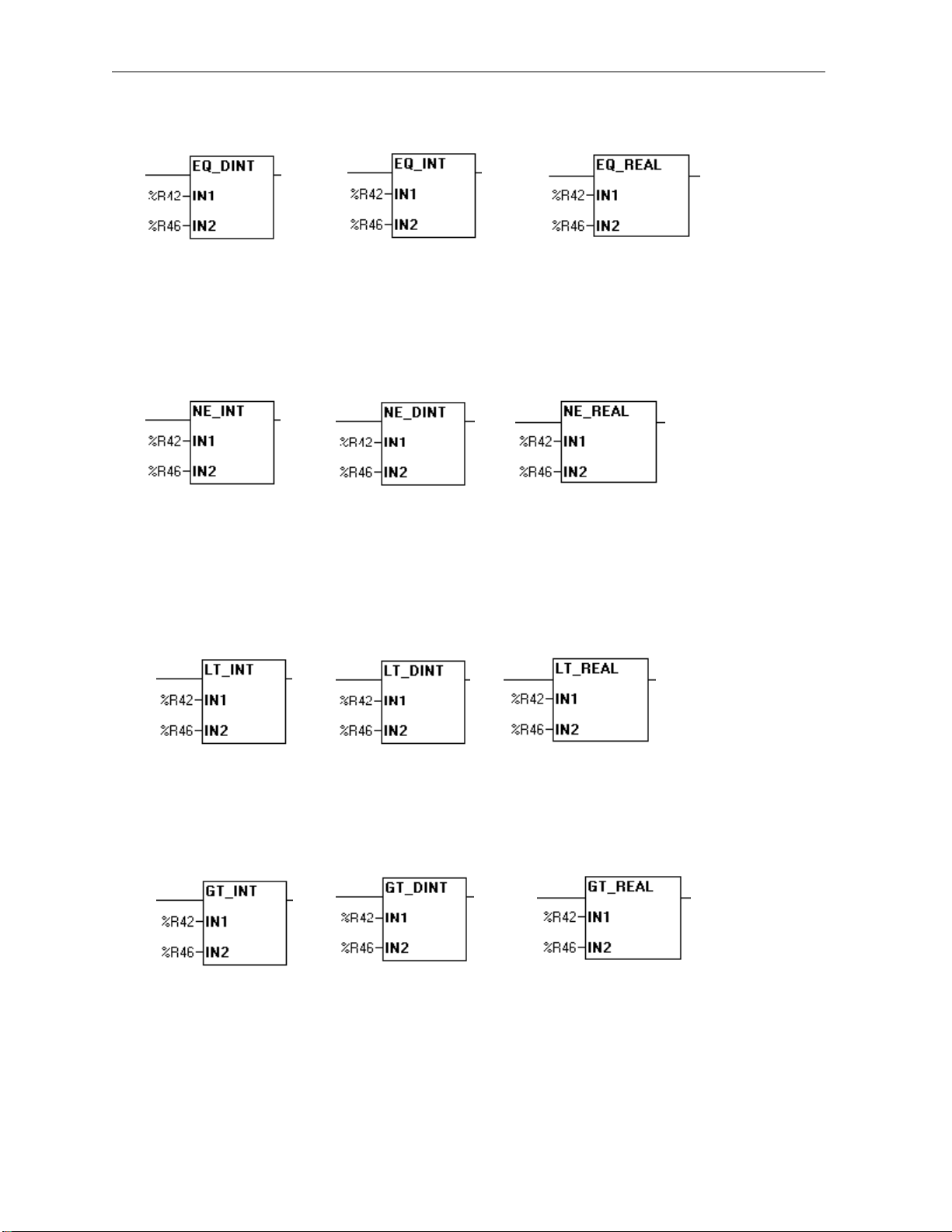
EQUAL
EQUAL DINT EQUAL1 REAL EQUAL
The EQUAL element compares two values, and passes powe r when the two values are equal in value.
The values can be constants or register type and offsets.
NOT EQUAL
INEQUALITY DINT NOT EQUAL1 REAL NOT EQUAL
The NOT EQUAL element compares two values and passes power when the two values are not equal in
value. The values can be constants or register type and offsets.
LESS THAN
LESS THAN DINT LESS THAN1 REAL LESS THAN
The LESS THAN element compares two values and passes power when IN1 is less than IN2. The
values can be constants or register type and offsets.
GREATER THAN
GREATER THAN DINT GREATER THAN1 REAL GREATER THAN.
The GREATER THAN element compares two values and passes power when IN1 is greater than IN2.
The values can be cons tant or register type and offsets.
Page 40
PAGE 40 17 SEP 2002 MAN0313-04
CH. 2
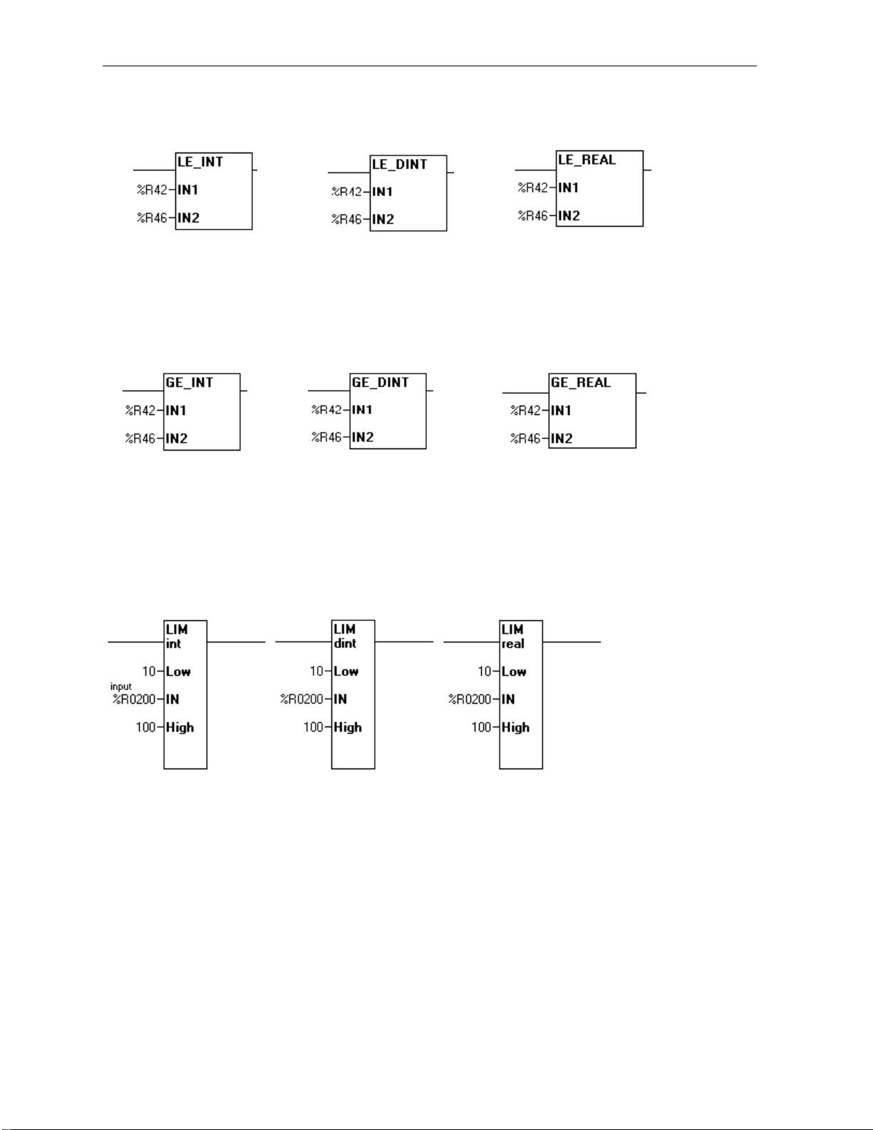
LESS THAN OR EQUAL
LESS THAN OR EQUAL DINT LESS THAN EQUAL1 REAL LESS THAN EQUAL
The LESS THAN OR EQUAL TO element comp ares two values and passes power when IN1 is less than
or equal to IN2. The values can be constant or register type and offsets.
GREATER THAN OR EQUAL
GREATER THAN DINT GREATER THAN EQUAL1 REAL GREATER THAN EQUAL
OR EQUAL
The GREATER THAN OR EQUAL TO element compares two values and passes power when IN1 is
greater than or equal to IN2. The values can be constant or register type and offsets.
LIMIT
Limit Function
Page 41
MAN0313-04 17 SEP 2002 PAGE 41
CH. 2
This functions determines if an input(IN) values is numerically in the range defined by the Low and High.
IN - This defines the Register Type and Offset (address) for comparison.
Low - This is either a constant or a Register Type and Offset (address) for the lower limit of
comparison.
High - This is either a constant or a Register Type and Offset (address) for the upper limit of
comparison.
If Low <= High:
This function passes power if the input is inside the range between Low and High (inclusive).
For example, if Low = 10 and High = 100 when the INPUT is between 10 and 100 the function passes
power. If the input is 9 or lower OR 101 or higher this function would not pass power.
If Low > High:
This function passes power if the input is outside the range between Low and High (inclusive).
For example, if Low = 100 and High = 10 when the INPUT is between 11 and 99 the function do es not
pass power. If the input is 10 or lower OR 100 or higher this function will pass power.
2.9 Program Control Jump, Label, Call, Return and End Elements :
2.9.1 Label Element
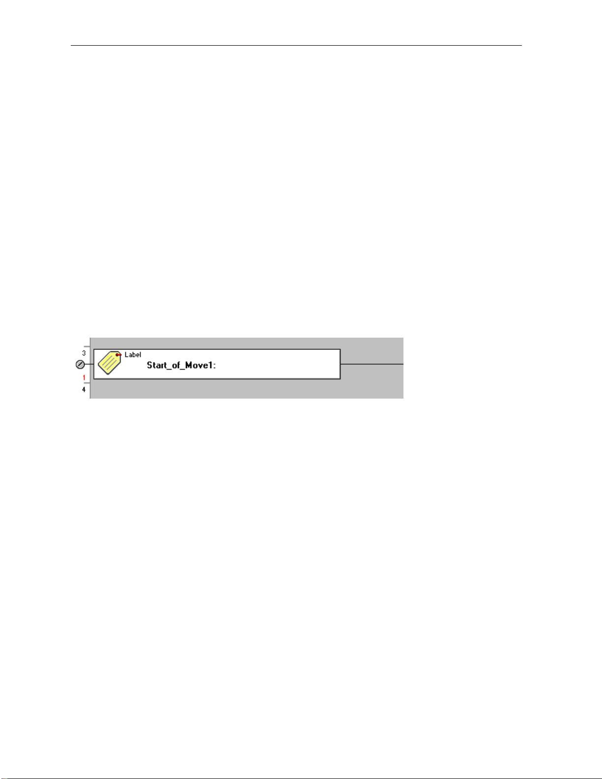
A label allows a position in the ladder program to be named. This name can be used with a JUMP or
CALL instruction to cause program execution to change from one section to another.
Note: There can only be one label with a particular label name in a program. Labels can be inserted
without matching jumps, but a jump must be matched with a label.
Page 42
PAGE 42 17 SEP 2002 MAN0313-04
CH. 2
2.9.2 Jump Element
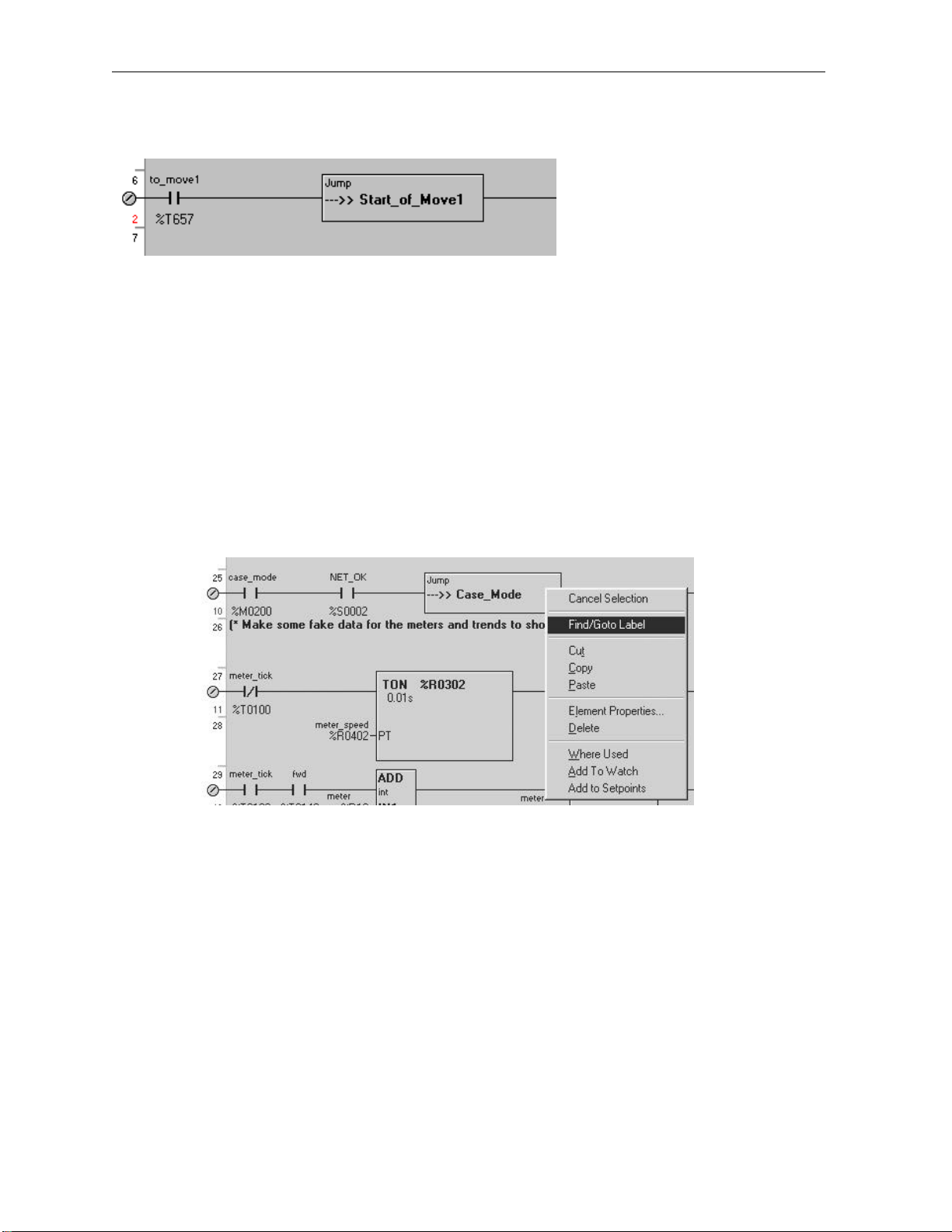
Use the JUMP element to cause a portion of the logic to be bypassed. The JUMP can be either aforward
or a backward JUMP. Logic execution will continue at the LABEL specified.
When the JUMP is active all coils within its scope are frozen. This includes coils associated with timers,
counters, relays...
No elements can be placed after the jump element. When the jump is active program execution jumps
directly from the jump element to the associated label.
Note: To avoid creating an endless loop with backward JUMP elements, a backwards JUMP must
contain a way to make it conditional.
To find the associated label, right -click on a Jump or Call:
Page 43
MAN0313-04 17 SEP 2002 PAGE 43
CH. 2
2.9.3 Call Element
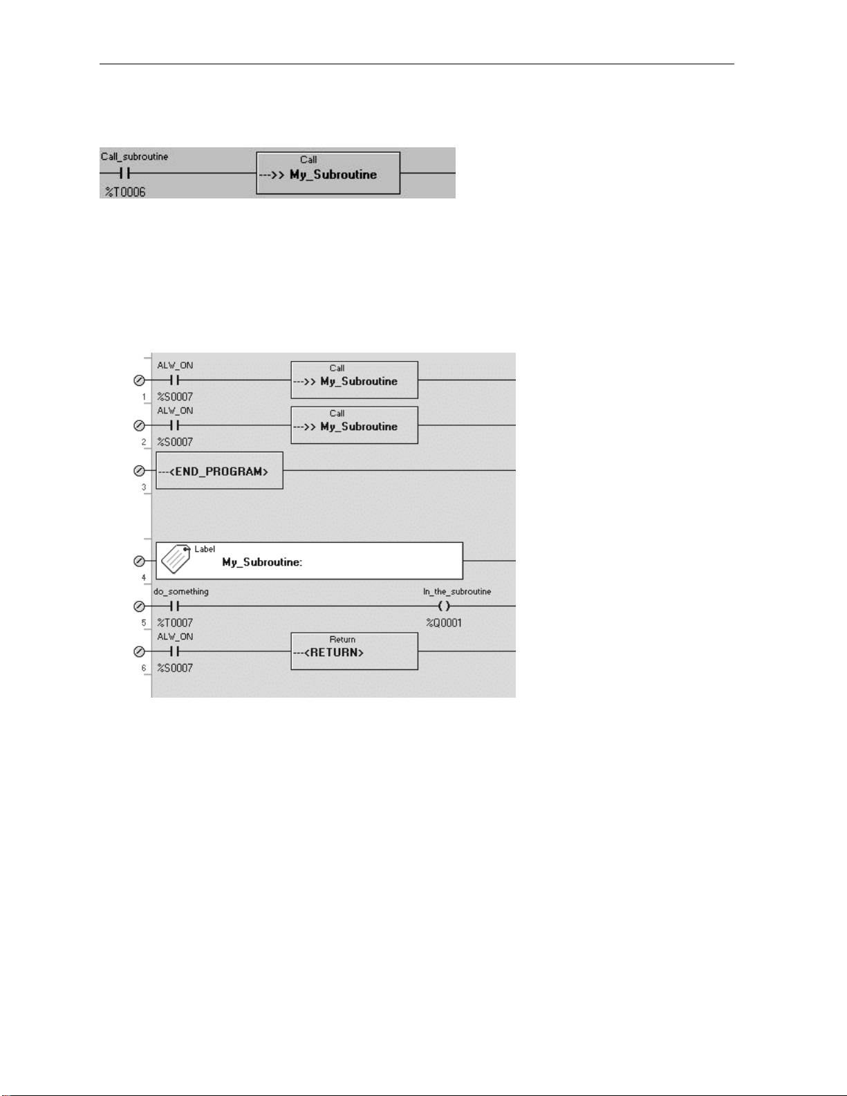
Use the CALL element to call a subroutine. If power flow into the CALL is on, execution will move to the
portion of ladder defined by a LABEL. When a RETURN element is executed in the subroutine, the
execution will resume on the rung following the CALL element. You can nest (calling a subroutine inside
a subroutine) up to 8 levels deep. If more than 8 levels of nesting are attempted, the controller will stop
and the logic error flag in the diagnostics will be set. No elements can be placed after a CALL element.
Example:
1. Start on rung 1, CALL the subroutine.
2. Execute first line of subroutine, rung 5 (rung 4 is only a LABEL indicating the start of a section).
3. Execute rung 6, the RETURN causes execution to start on the rung after the last CALL, rung 2.
4. Execute rung 2, CALL the subroutine again.
5. Execute first line of subroutine, rung 5 (rung 4 is only a LABEL indicating the start of a section).
6. Execute rung 6, the RETURN causes execution to start on the rung after the last CALL, rung 3.
7. Execute rung 3, END PROGRAM ends this scan. After I/O and other processing start over at
rung 1.
Page 44
PAGE 44 17 SEP 2002 MAN0313-04
CH. 2
2.9.4 Return Element
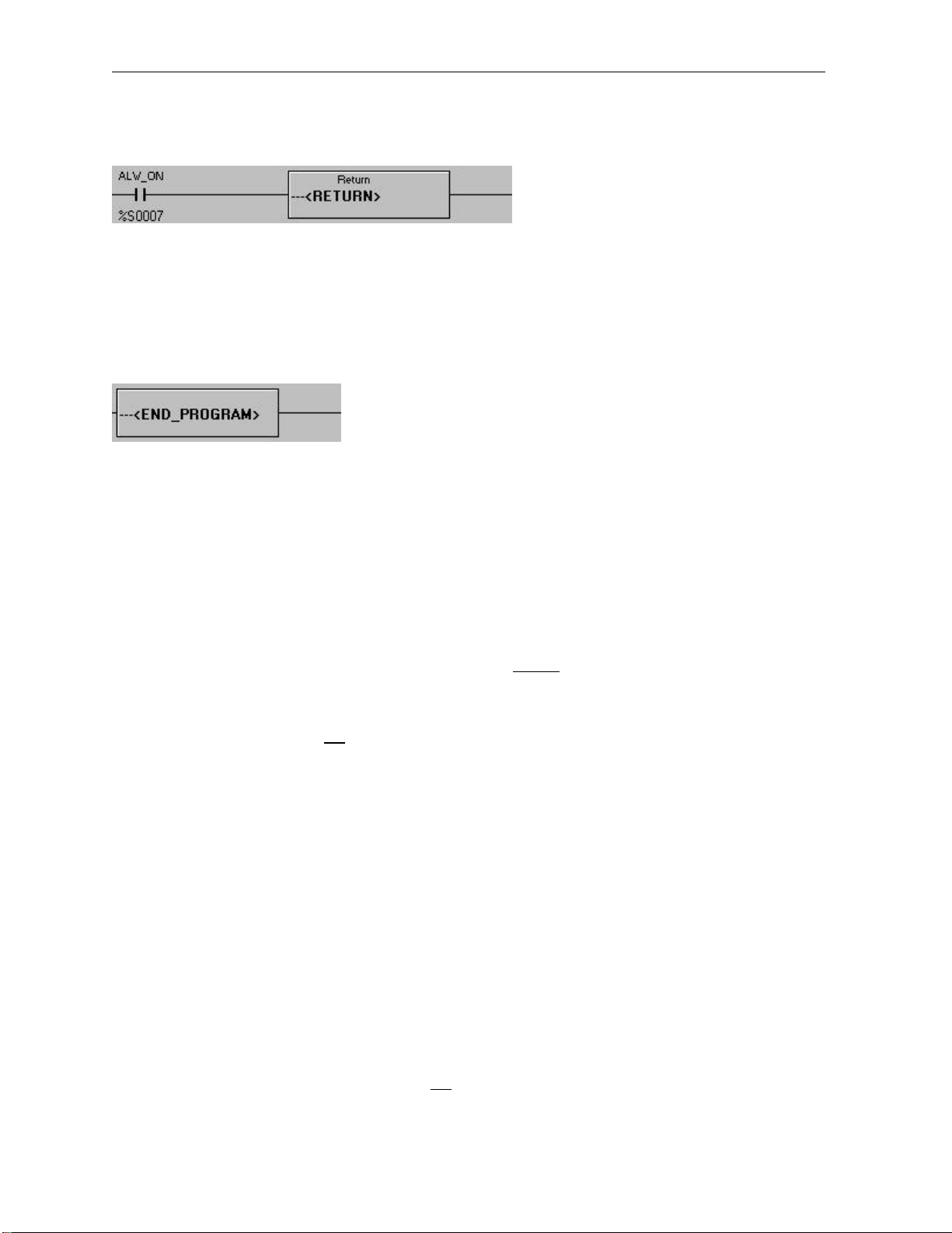
Use the RETURN element to return from a subroutine call. If power flow is enabled, this will return ladder
execution to the rung following the last CALL. If a RETURN is executed without a CALL, the controller
will stop and the Logic Error diagnostic flag will be set. No elements can be placed after a RETURN
element.
2.9.5 End Program Element
Use this element to end the program scan. Th is element does not need a contact before it. When this
element is executed the scan is immediately finished, I/O is read, other housekeeping is performed and
another scan is started. This can be used to separate a main section of ladder from subroutin es as seen
in the example above, or can be used to temporarily disable a portion of the ladder program for testing.
2.10 Conversion Elements
2.10.1 General
Conversion elements are included to provide an easy method to convert between different data types.
The primary data types are INT (16-bit), DINT (32-bit), and REAL (32-bit). Conversions are necessary, for
example, when an analog input value needs to be converted from Double Integer type to Real type before
engineering unit (EU) formulas are applied.
NOTE: Numeric constants are not allowed in either the Source nor Destination fields.
2.10.2 Caveats of Conversion
Conversion is made by value - not storage size. All INT values can be converted to DINT or REAL. Some
DINT (32-bit) values can be successfully converted to INT (16-bit) format. Some REAL (32-bit) values
can be converted to DINT (32-bit) or INT (16-bit).
NOTE: It is the programmers responsibility to ensure that all expected values fit into the destination
register's size and format.
In some cases, precision can be lost. If, for example, when converting a DINT to REAL the DINT contains
7 digits (" 2123789") the REAL value is truncated to the six-digit precision used by Real Numbers
("2.12378E+06").
Data can be lost. When converting REAL to INT or DINT, any fractional part of the number is rounded.
(REAL)1.23654E+02 = (INT)124.
Such losses are NOT considered errors. The element continues to function normally, but downstream
elements, which depend on these values, can not produce the expected results.
Page 45
MAN0313-04 17 SEP 2002 PAGE 45
CH. 2
It is an error to attempt to convert a large number into a type, which can contain that number. This occurs
most often when converting DINT to INT but can also occur when converting REAL to either INT or
DINT.
If this overflow occurs there is no power flow through the element, and the result is undefined.
2.10.3 Configuring Conversion Elements
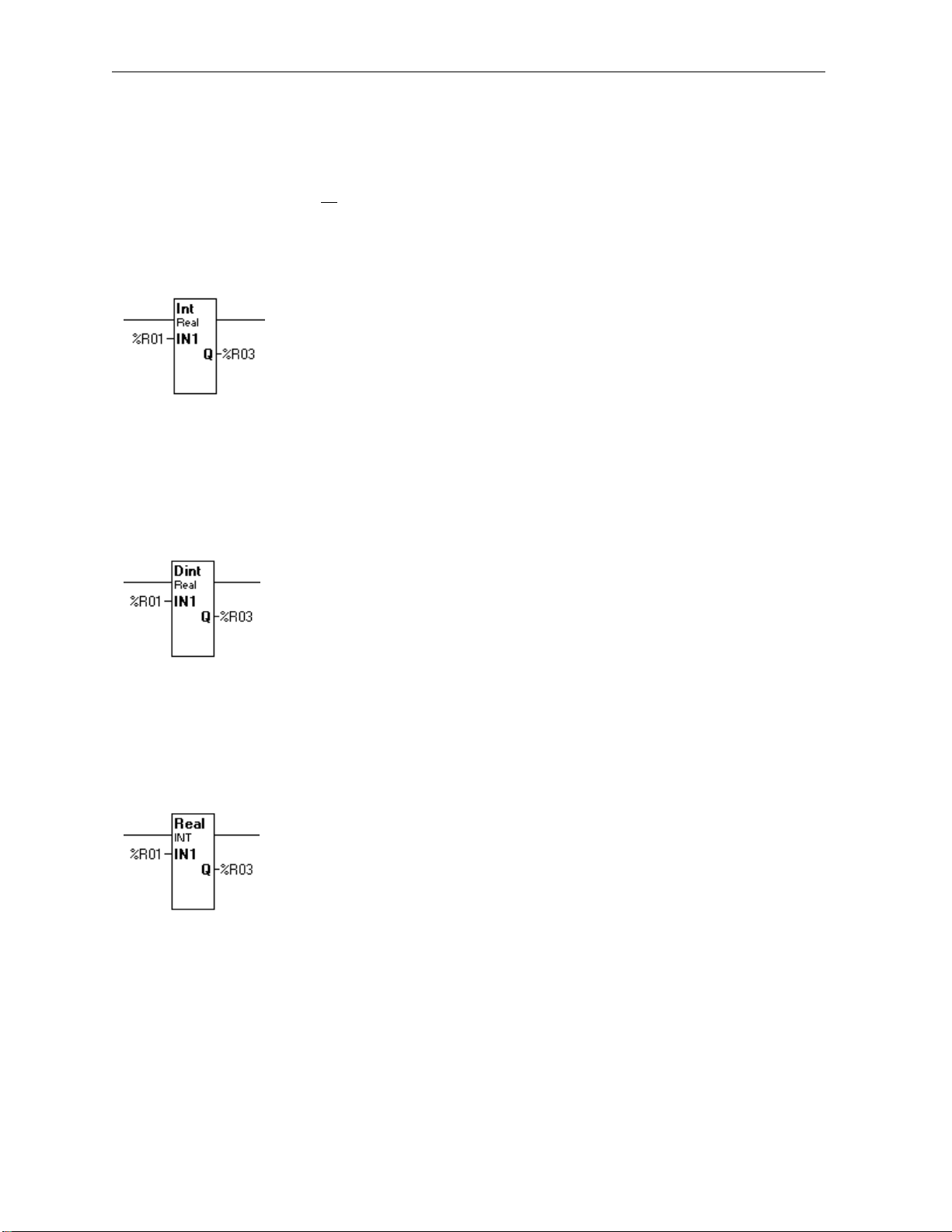
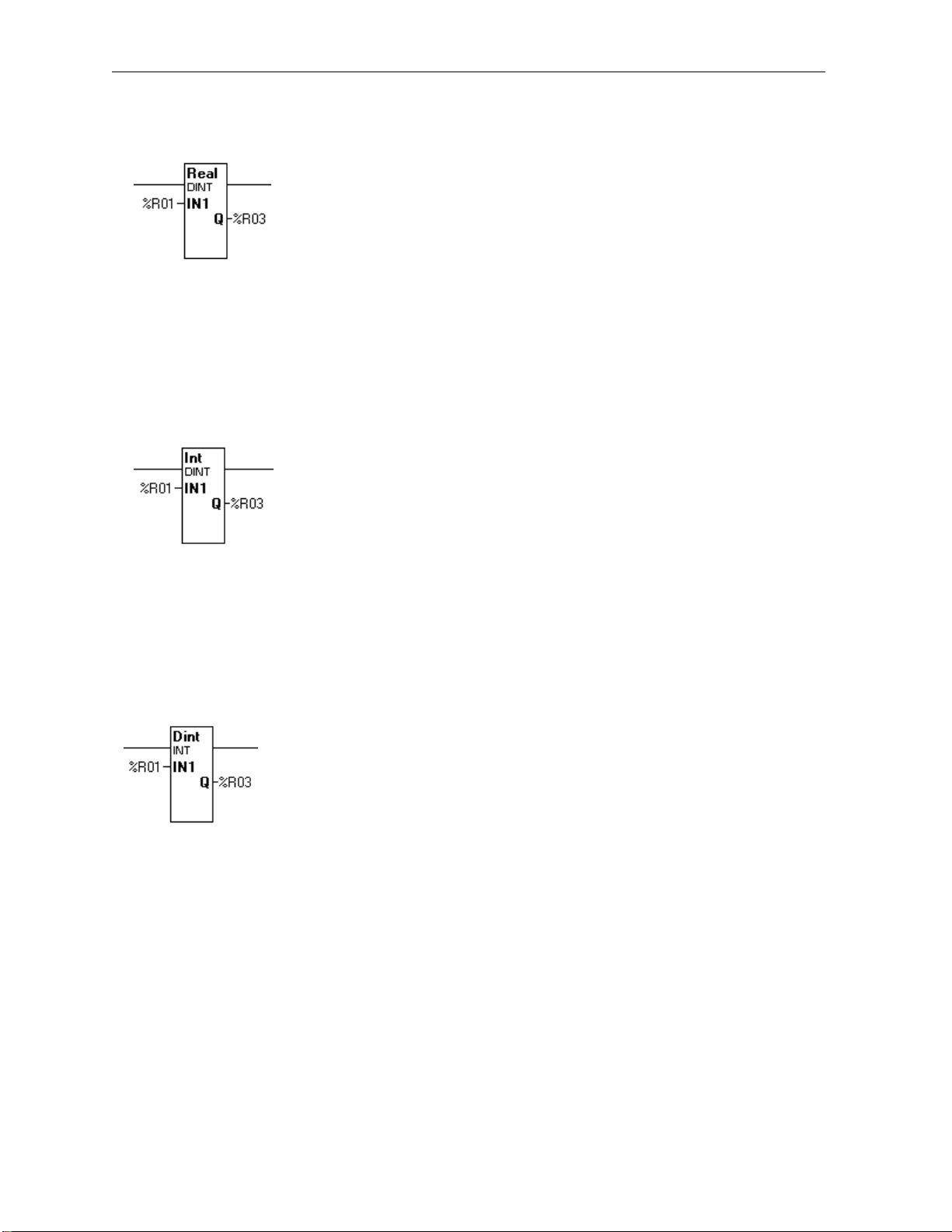
INTEGER TO REAL
Conversion Int To Real
This converts the INT (16 -bit) value in IN1 to a REAL (32-bit) value in Q. Note that IN1 is a 16-bit value
and Q is a 32-bit value.
DOUBLE INTEG ER TO REAL
Conversion Dint To Real
This converts the DINT (32 -bit) value in IN1 to a REAL (32-bit) value in Q. Note that IN1 is a 32-bit value
and Q is a 32-bit value.
REAL TO INTEGER
Conversion Real To Int
This converts the REAL (32 -bit) value in IN1 to a INT (16-bit) value in Q. Note that IN1 is a 32-bit value
and Q is a 16-bit value.
Page 46
PAGE 46 17 SEP 2002 MAN0313-04
CH. 2
REAL TO DOUBLE INTEGER
Conversion Real To Dint
This converts the REAL (32 -bit) value in IN1 to a DINT (32-bit) value in Q. Note that IN1 is a 32-bit value
and Q is a 32-bit value.
INTEGER TO DOUBLE INTEGER
Conversion Int To Dint
This converts the INT (16 -bit) value in IN1 to a DINT (32-bit) value in Q. Note that IN1 is a 16-bit value
and Q is a 32-bit value.
DOUBLE INTEGER TO INTEGER
Conversion Dint To Int
This converts the DINT (32 -bit) value in IN1 to a INT (16-bit) value in Q. Note that IN1 is a 32-bit value
and Q is a 16-bit value.
Page 47
MAN0313-04 17 SEP 2002 PAGE 47
CH. 2
2.11 Timer and Counters
The timers and counters are control register based. Each element requires two (2) consecutive
registers.
Configuring Timer Elements
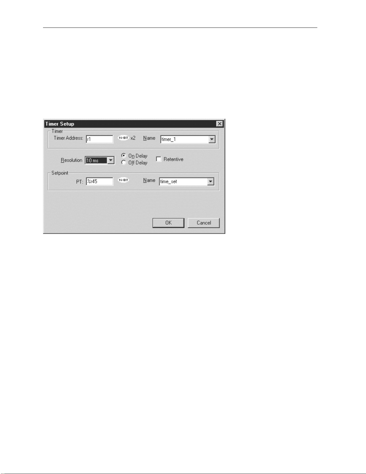
To configure the element, double click it, and then select the proper values from the configuration dialog
box.
Configuring Timer Elements
Timer Address - Type in the Register Type and Offset to be used by this timer. Each timer requires two
(2) consecutive addresses.
PT (Setpoint) - This is the timeout period expressed in timebase units. For example, if the resolution
(timebase value) is 100 milliseconds and the timeout value is "20", the timeout period is 2000 milliseconds
or 2 seconds. This entry can also use a Register reference.
Resolution - This is the timebase value. Use the drop -down list to select either 10 milliseconds or 100
milliseconds.
Page 48
PAGE 48 17 SEP 2002 MAN0313-04
CH. 2
On Delay/Off Delay - This selec ts the action of the timer.
Retentive - Only the ON DELAY TIMER can be marked as retentive. (Covered later in this section.)
Reset Input Address - If the timer is retentive, this defines the Register Type and Offset used to
reset the timer. This box appears only if the timer is retentive.
Reset Input Name - If the timer is retentive , this defines the Register used to reset the timer can be
selected by name. This box appears only if the timer is retentive.
Register Usage
Each Timer/Counter requires two (2) consecutive 16 -bit registers (%R). They are arranged like so
%Rx Accumulator
%Rx+1 Power Enabled Reserved
Bit 16 Bit 15 Bits 14 - 1
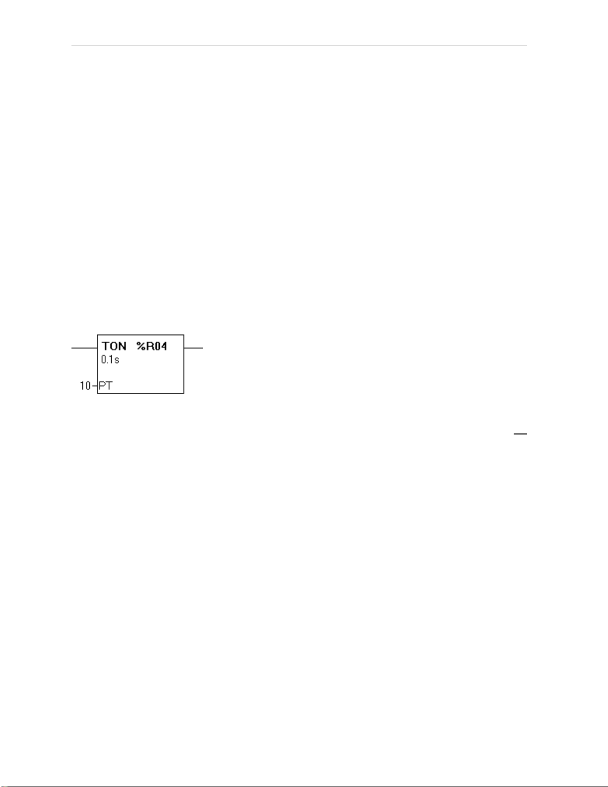
On Delay Timer
Timer On Delay
Note: Only the On Delay Timer is retentive. (When power flow is removed from the element, it does not
clear the elapsed time.)
When power is supplied to the TON the output becomes inactive and the TON counts up to the preset
value at a rate determined by the configured timebase. When the internal accumulator reaches the
Preset Value, the output becomes active and counting stops.
When power is removed from the element, the TON resets to zero.
Page 49
MAN0313-04 17 SEP 2002 PAGE 49
CH. 2
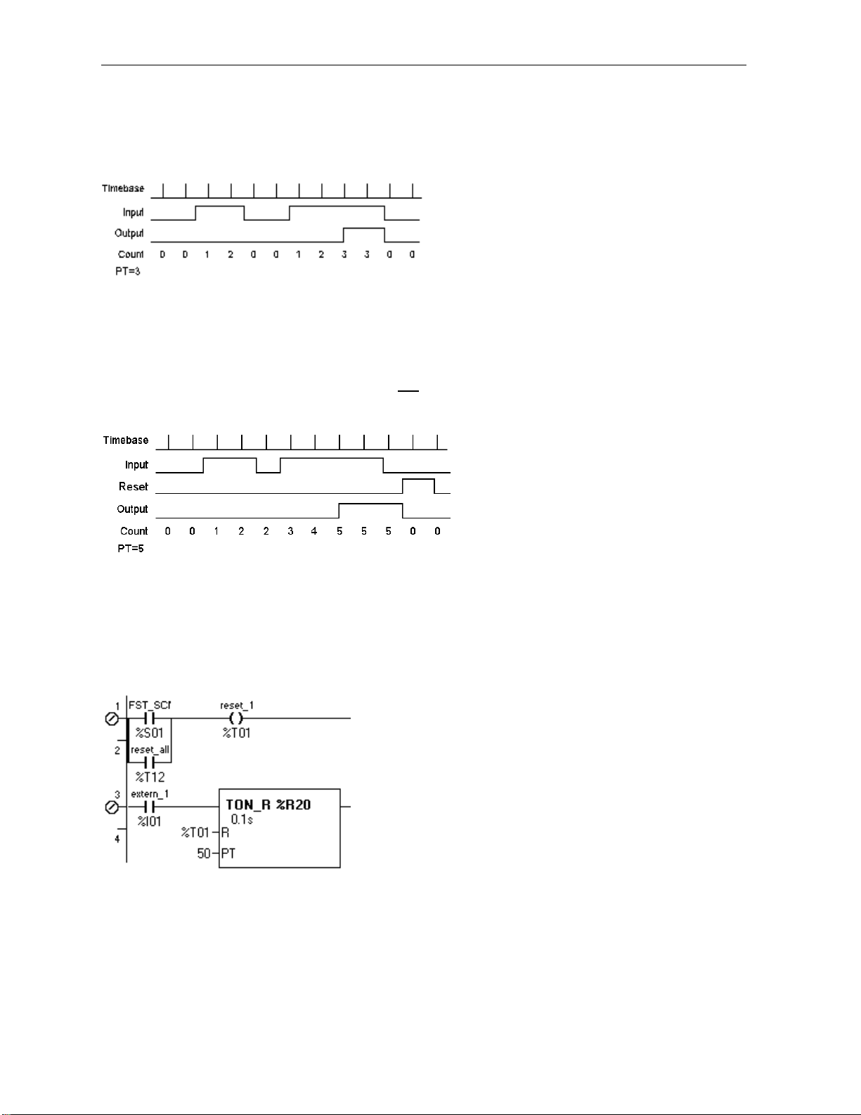
The timebase is user definable in 10mS or 100mS "ticks". When power is applied to the element,
counting proceeds using this timebase.
ON Delay Timer Diagram
Retentive On Delay Timer
A Retentive On Delay Timer is a special case of the "standard" On Delay Timer, but differs from the
standard timer in that the Retentive Timer does not reset when the input is brought inactive (off). The
Retentive Timer requires that a reset signal be applied to the element in order for the timer to be reset.
Retentive On Delay Timing Diagram
Note: Resetting the Retentive Timer requires the use of a contact under software control of the
controller.
Since the Retentive Timer is retentive, any value appearing in registers assigned to the eleme nt can be
invalid immediately after a down load. One approach is to reset the timer in combination with the First
Scan bit:
Example Reset Retentive Time
Page 50
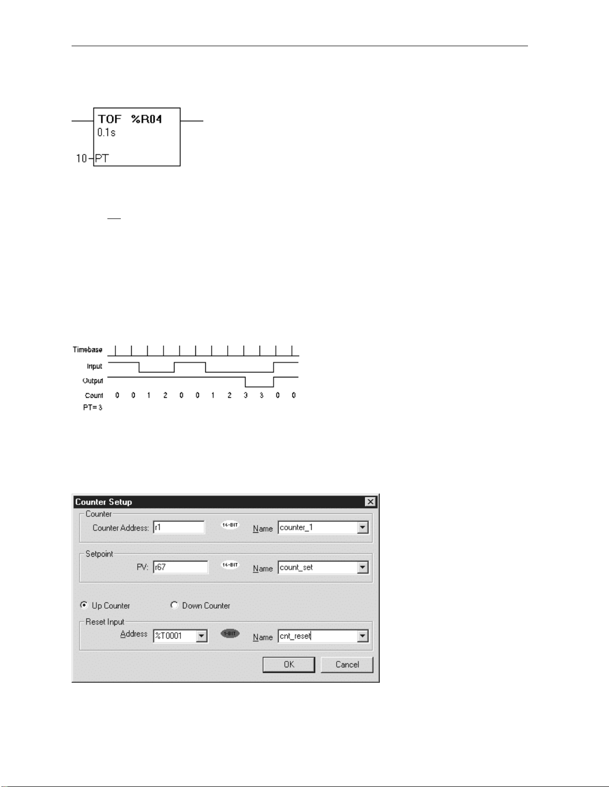
PAGE 50 17 SEP 2002 MAN0313-04
CH. 2
Off Delay Timer
Timer OFF Delay
NOTE: Only the On Delay Timer may be retentive (when power flow is removed from the element it does
not clear the elapsed time).
When power is removed from the TOF the output becomes active, and the TOF counts up to the preset
value at a rate determined by the configured timebase. When the internal accumulator reaches the
Preset Value, the output becomes inactive and counting stops.
When power is supplied to the element, the TOF resets to zero.
The timebase is user definable in 10mS or 100mS ticks. When power is applied to the element, counting
proceeds at this timebase.
OFF Delay Timing Diagram
Configuring Counter Elements
To configure the element, double click it, and then select the proper values from the configuration dialog
box.
Counter Setup
Page 51
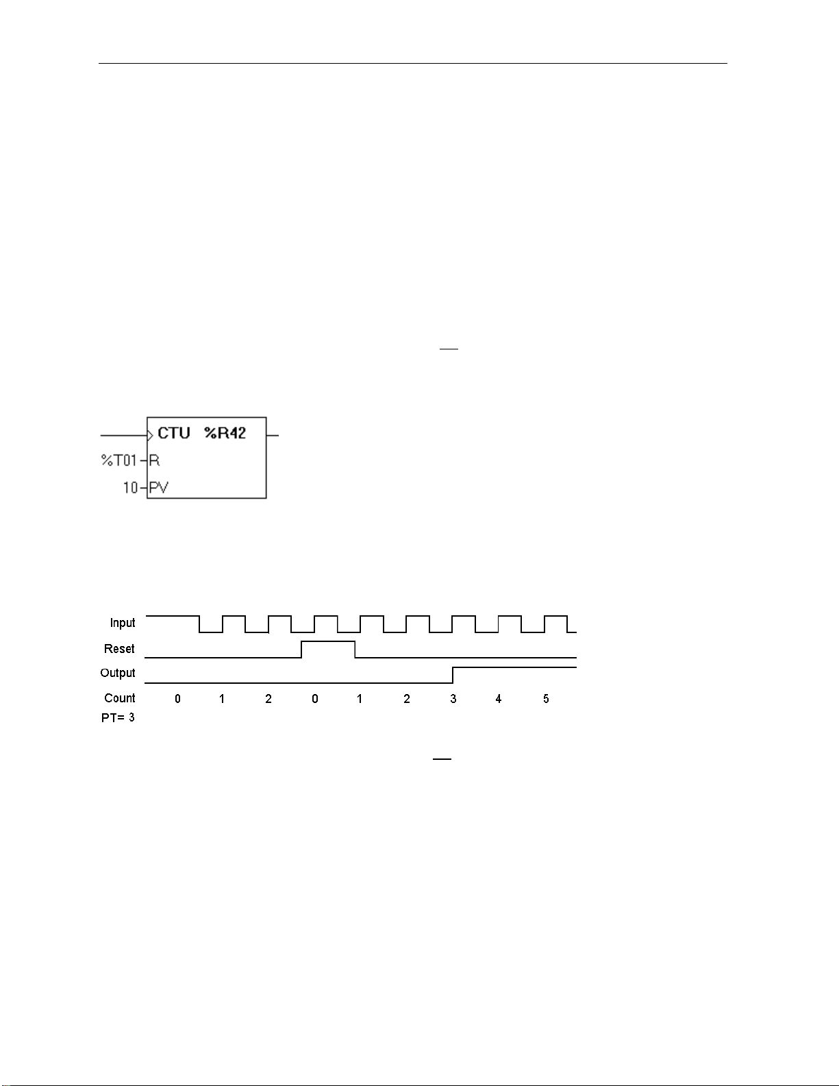
MAN0313-04 17 SEP 2002 PAGE 51
CH. 2
Counter Address - Type in the Register Type and Offset to be used by this timer. Each counter
requires two (2) consecutive addresses.
PV (Setpoint) - This is the preset value for the counter. When the counter reaches this value, its output
becomes TRUE, thus passing power to any other elements on this rung.
Up Counter/Down Counter - This determines the direction of count - UP or DOWN.
Reset Input Address - This determines which point is used to reset the timer. This should be a Boolean
point. In this box, select the Register `Type and Offset.
Reset Input Name - If the point used to reset the timer has already been named (highly recommended )
one can select it by name rather than by Type and Offset.
NOTE: The Reset Input must be configured even if it is not used.
Counter Operation
Counter Operation
The counter counts inactive-to-active transitions of its input power. When the count reaches some preset
value, the output becomes active, but the counter continues to count input pulses. The Counter can be
reset at any time by applying power to the Reset input.
Note: The Reset Input mus t be configured even if it is not used.
Page 52

PAGE 52 17 SEP 2002 MAN0313-04
CH. 2
2.12 Shift and Rotate Elements
Note: Shift and Rotate Elements operate on WORD Integer (16 -bit) DWORDS.
2.12.1 General
Operations are performed on the bit patterns of the register. After the operation, the results are stored in a
result register. The input register is not changed.
Power flow through the SHIFT elements is determined by the last bit shifted out of the register.
For example, if %R41 contains 21770 (0101010100001010) and the number of shifts is 4, then:
Shift Power
Flow
0 0 010101010000101
1 0 101010100001010
2 0 010101000010100
3 0 101010000101000
4 1 010100001010000
The power output is determined after the last shift. Any preceding bits do not affect the power output and
are lost.
Power flow through the ROTATE elements is always TRUE regardless of the state of the last bit rotated
out.
2.12.2 Configuring Shift and Rotate Elements
To configure the element, double click it, and then enter the Register Type and Offset for the input
register, the output register, and the shift count ("N").
Values for the Input and Shift Count ("N") can also be fixed INT or DINT values. The Output ("Q") must
be a Register Reference (%R, etc).
These elements work on 16-bit or 32-bit registers.
NOTE: With a Shift Element referencing a Word register, a shift count (N) larger than 15 loads all bits in
the register with 0. With a Rotate Element, a shift count (N) of 16 returns the value to its original state.
With a Shift Element referencing a DWord register, a shift count (N) larger than 31 loads all bits in the
register with 0. With a Rotate Element, a shift count (N) of 32 returns the value to its original state.
Value
(unshifted)
Page 53
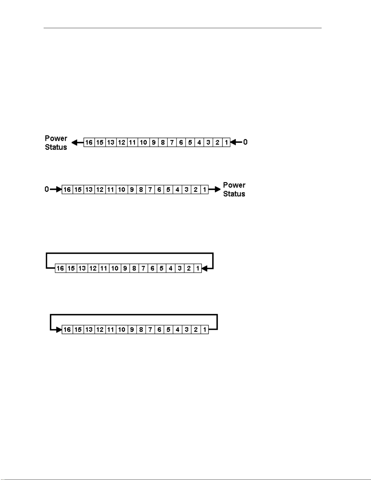
MAN0313-04 17 SEP 2002 PAGE 53
CH. 2
2.12.3 Shift vs. Rotate
The difference between the two functions is the use of the data that is shifted out.
In the SHIFT functions, shifted out data is lost, except for the bit shifted out during the final shift, which is
then used as the power status of the element. This determines whether or not power is passed through
the element. If a 0 bit is the last bit shifted out power is not passed through the element. If the last bit
shifted out is 1 power is passed through the element.
SHIFT LEFT
SHIFT LEFT
SHIFT RIGHT
SHIFT RIGHT
In the ROTATE functions the shifted out data is re -circulated back to the other end of the data field. No
data is lost. It is rotated into the other end of the field.
ROTATE LEFT
ROTATE LEFT
ROTATE RIGHT
ROTATE RIGHT
Page 54
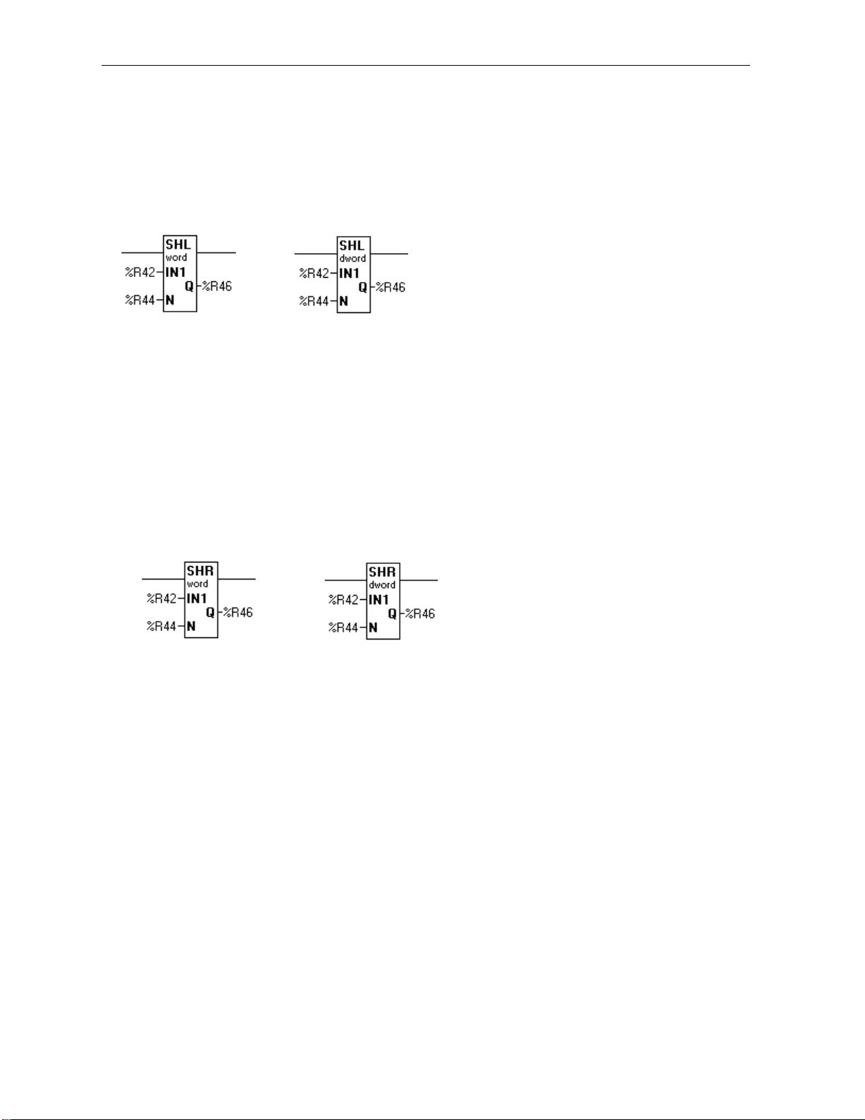
PAGE 54 17 SEP 2002 MAN0313-04
CH. 2
BITWISE SHIFT LEFT
This element performs a LOGICAL SHIFT LEFT on the input register, and places the result in the output
register. During the shift, 0 bits are shifted into the right end of the value. The value is shifted by N
counts. Both IN1 and N can be either register designation (%R, %AI, etc) or integer values (8, 23). Q
must be a Register Offset Address.
BITWISE SHIFT LEFT DWORD SHIFT LEFT
%R41 = 0000000100010000 (544)
SHL 8 %R43 = 0001000000000000 (4096)
Power Flow = ON (TRUE)
BITWISE SHIFT RIGHT
This element performs a LOGICAL SHIFT RIGHT on the input register and places the result in the output
register. During the shift, 0 bits are shifted into the left end of the value. The value is shifted by N counts.
Both IN1 and N can be either register designation (%R, %AI) or integer values (8, 23). Q must be a
Register Offset Address.
BITWISE SHIFT RIGHT DWORD SHIFT RIGHT
%R41 = 1000000000000000 (32768)
SHR 8 %R43 = 0000000010000000 (128)
Power Flow = OFF (FALSE)
Page 55
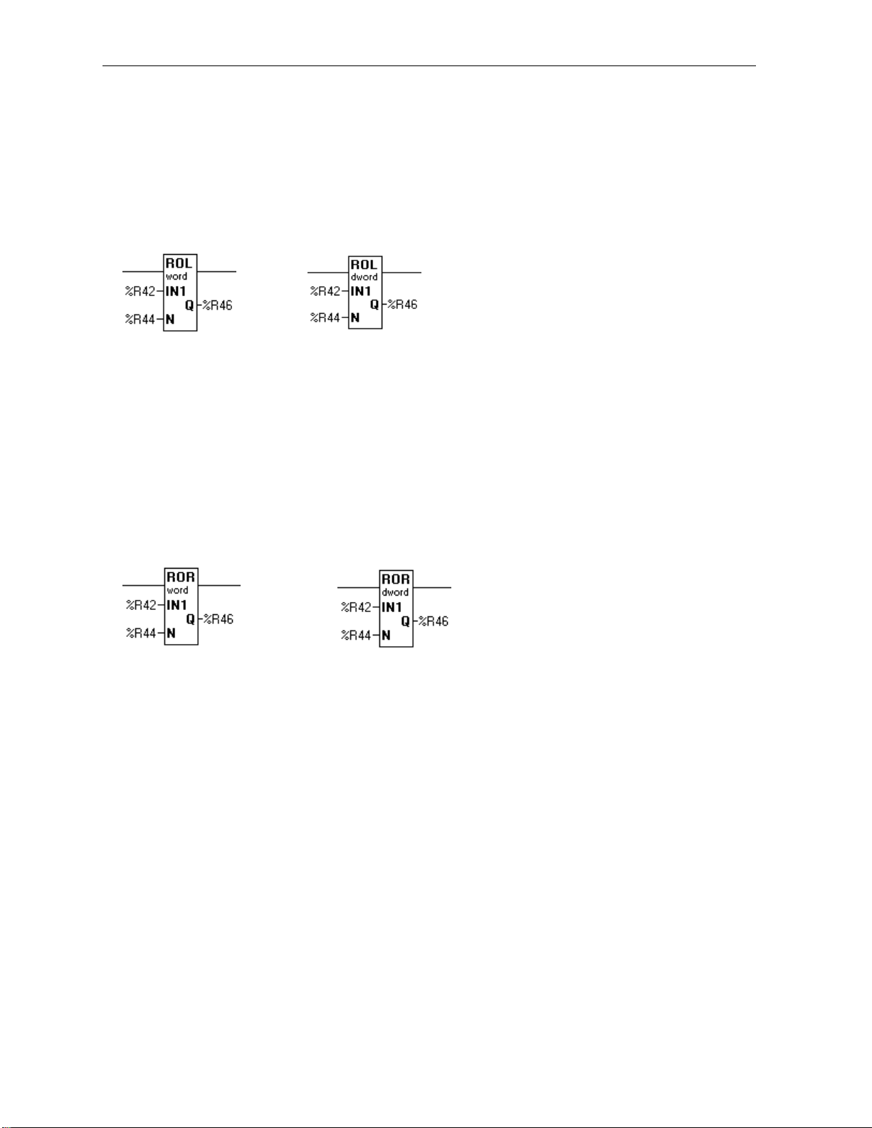
MAN0313-04 17 SEP 2002 PAGE 55
CH. 2
BITWISE ROTATE LEFT
This element performs a ROTATE LEFT on the input register, and places the result in the output register.
During the shift, the "output bit" is returned to the first bit on the right end of the value. The value is shifted
by N counts. Both IN1and N may be either register designation (%R, %AI, etc) or integer values (8, 23,
etc). Q must be a Register Offset Address.
BITWISE ROTATE LEFT DWORD ROTATE LEFT
%R41 = 1010010100111100 (42300)
ROL 11 %R43 = 1110010100101001 (58665)
BITWISE ROTATE RIGHT
This element performs a ROTATE RIGHT on the input register, and places the result in the output
register. During the shift, the output bit is returned to the first bit on the left end of the value. The value is
shifted by N counts. Both IN1 and N can be either register designation (%R, %AI) or integer values (8, 23).
Q must be a Register Offset Address.
BITWISE ROTATE RIGHT DWORD ROTATE RIGHT
%R41 = 1010010100111100 (42300)
SHR 11 %R43 = 1010011110010100 (42900)
2.13 Data Move Elements
2.13.1 Single Data Moves
Data Move elements allow the movement of data between registers (i.e, read an Analog Input [%AI]) and
place it into a storage register, %R. Data Moves can also be used to move constant values into registers,
move blocks of data from one location to another or to fill a block of registers with the same value.
The values in the source registers are not changed except if, during a Block Move or Block Fill element,
the operation of the element overwrites the source register.
Page 56

PAGE 56 17 SEP 2002 MAN0313-04
CH. 2
a. Type Checking
There is no type checking. Values are moved in a bit-wise fashion without regard to the type or polarity of
the source nor destination. The Block Move instructions can be used to move WORD, DWORD or REAL
value from source to destination. Note that each DWORD or REAL value moves two (2) WORD registers.
b. Power Flow Through The Element
Power flow through the element is always TRUE after the element completes.
The exception to this is the Indirect Move Element. In this case, the move is considered invalid and
power flow is FALSE if either the source or destination register contains 0 (zero) or the length of the move
exceeds the number of elements available in the controller.
c. Configuring Data Move Elements
To configure the element, double click it, and enter the element, double-click it, and enter the
Register Ty pe and Offset (address) for the input and output registers.
For the Register Move and Block Fill elements, a numeric constant can be specified as the SOURCE. In
this case, the numeric value is placed into the output register. The DESTINATION must be specified using
Register Type and Offset addressing.
For the Block Move element, SOURCE and DESTINATION must be Register type and Offset addresses.
Neither can be a numeric constant. The COUNT value determines how many registers are moved or filled
during the operation of this single element.
In the case of the Register Move instruction the Count value is fixed at 1. For the Block Move and Block
Fill elements, the COUNT value can be a number in the range of 0 (zero) to the maximum number of
registers of this type available in this controller. For %R registers in the OCS products, the upper limit is
2048.
For the Move Word element, selected the Data Type (WORD) or DWORD) to be moved.
SINGLE REGISTER MOVE
NOTE: Move_Word can operate on either 16 -bit or 32-bit data, as selected by the user.
This moves either a register or register pair (32 -bit) or a constant value into another register or register
pair (32 -bit).
a. MOVE WORD
Page 57
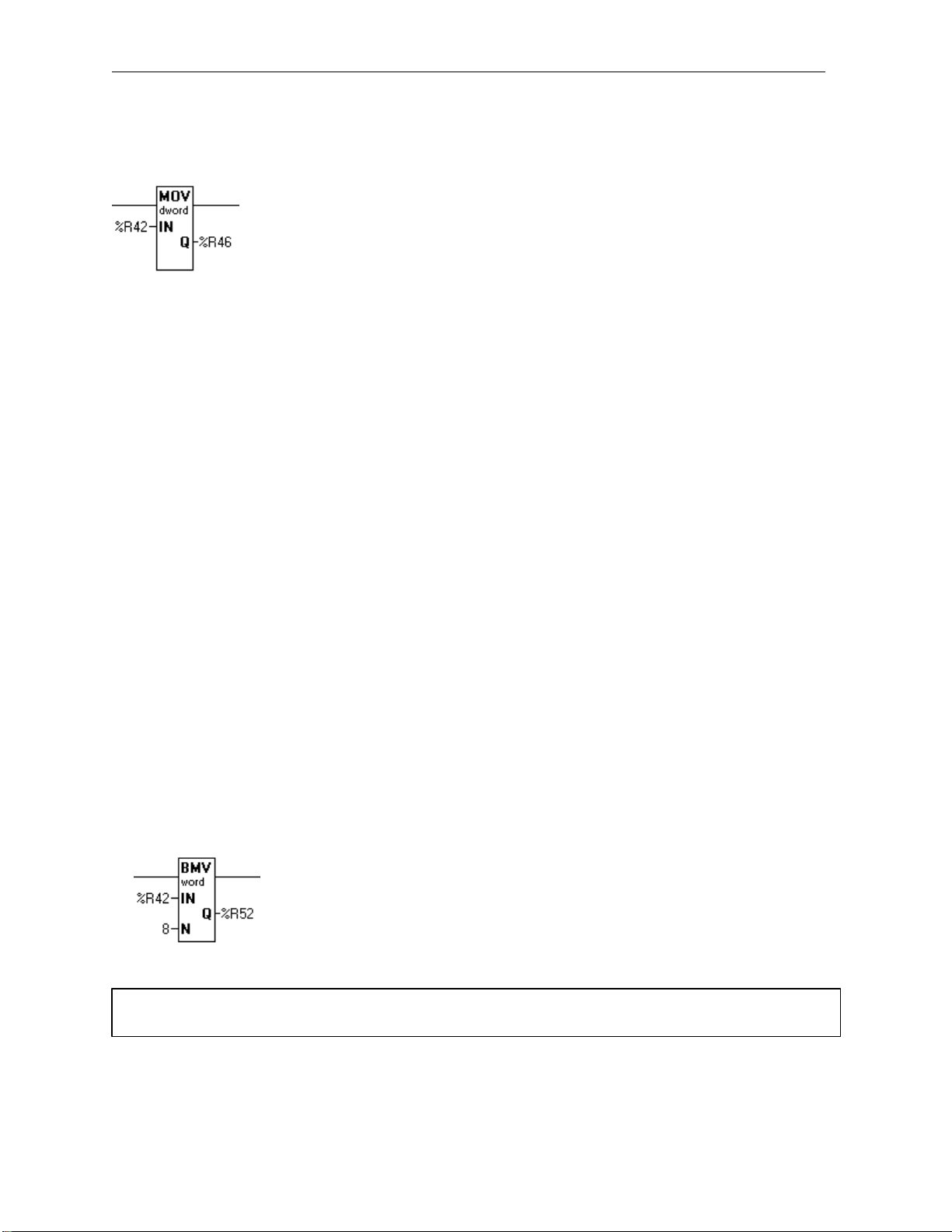
MAN0313-04 17 SEP 2002 PAGE 57
WARNING: If the IN value is a signed numeric constant, it is treated as an unsigned number when the
CH. 2
b. MOVE DWORD
During configuration from the Type box, select either WORD (16-bit) or DWORD (32-bit).
For example, if before the element is performed, the registers contain:
%R42 34567
%R43 12
%R44 63
%R45 127
%R46 82
After the element is finished, the registers contains
%R42 34567
%R43 12
%R44 63
%R45 127
%R46 34567
The IN value can also be configured as an unsigned numeric constant. For example if IN is configured
as the value 1492, register %R46 contains the value 1492 after the element completes.
WARNING: If the IN value is a signed numeric constant, it is treated as an unsigned number when the
element is configured. For example, if IN is configured as -1, the value 65535 is used.
For DWORD (32-bit) Moves, two sequential registers are effected. For example, if the value in %R42and
%R43 is 103582, registers %R44and %R45 contain the value 103582 after the element is completed.
BLOCK REGISTER MOVE
NOTE: The Block_Move element operates on 16-bit data only.
This element moves a block of registers from one location to another location.
BLOCK MOVE WORD
element is configured. For example, if IN is configured as -1, the value 65535 is used.
Page 58
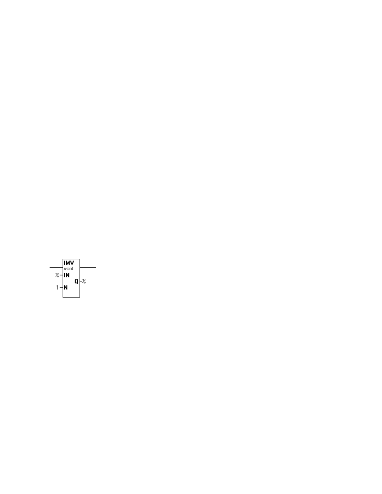
PAGE 58 17 SEP 2002 MAN0313-04
CH. 2
Using the above illustration as an example, if before the element is performed, the registers contain:
%R42 65535 %R50 0
%R44 65535 %R51 0
%R44 65535 %R52 0
%R45 65535 R53 0
%R46 65535 %R54 0
%R47 65535 %R55 0
%R48 65535 %R56 0
%R49 65535 %R57 0
After the element is finished the registers contain:
%R42 65535 %R50 65535
%R44 65535 %R51 65535
%R44 65535 %R52 65535
%R45 65535 %R53 65535
%R46 65535 %R54 65535
%R47 65535 %R55 65535
%R48 65535 %R56 0
%R49 65535 %R57 0
INDIRECT MOVE
NOTE: The Indirect_Move element operates on 16-bit data only.
Operation of this element is similar to the Block_Move instruction. A block of data is moved from one
location in memory to another.
MOVE INDIRECT
Refer to Power Flow Through the Element.
The difference, though, is how the element obtains the address of the source block (IN), the destination
block (Q) or both. In this case, one has the option of specifying the address directly in Register Type and
Offset format or indirectly.
With the Indirect format , the register specified contains the offset of the first %R register to be moved. In
the case of the destination, the register contains the address or offset of the first %R register of the
destination block.
NOTE: Indirect addressing uses only to %R registers. The source or destination register itself can be any
register. Any re gister can be specified if the INDIRECT box is unchecked.
Page 59
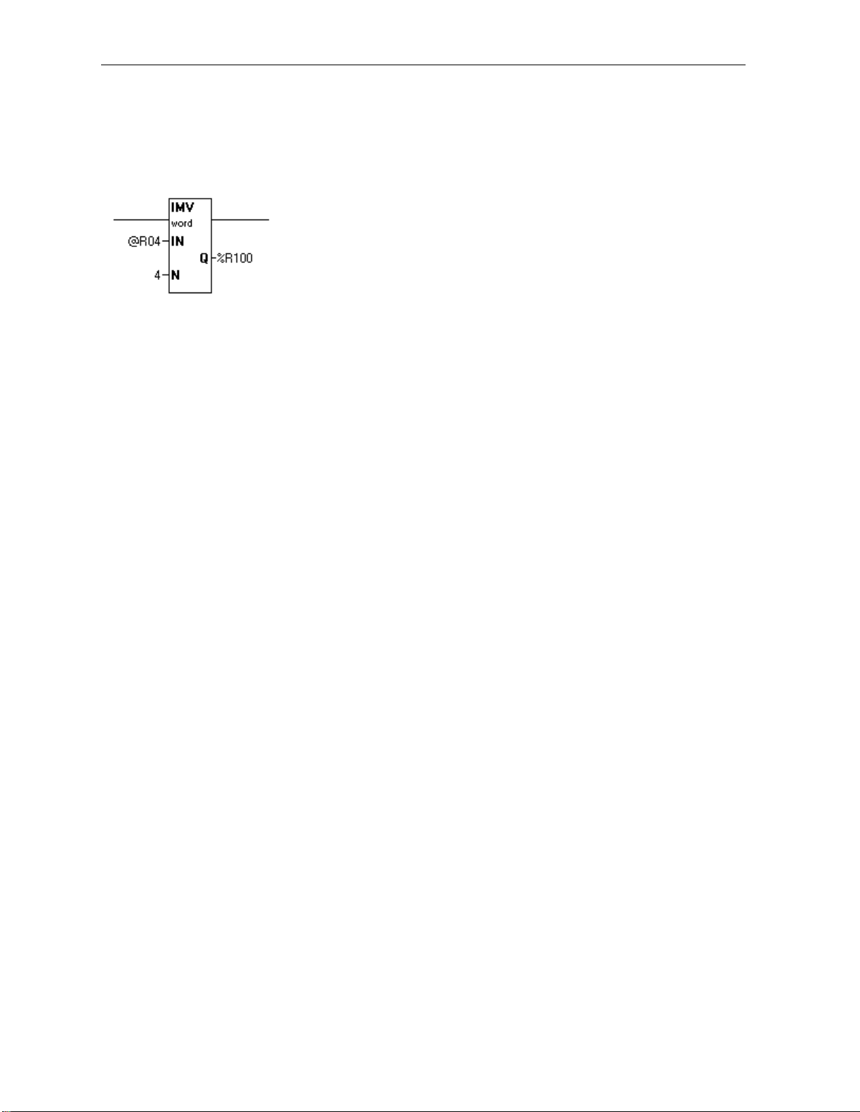
MAN0313-04 17 SEP 2002 PAGE 59
CH. 2
Either IN, Q or both can be direct or indirect. Constant values, however, are not allowed.
For example, configure the element such that IN is %AI1, Q is %R12, and both indirect boxes are
checked, and that four (4) words are to be moved. The configured element appears:
INDIRECT MOVE
Note the use of the special @ character indicating that the associated register is used as an indirect
value.
When this element receives power, the value is taken from %AI1 and used as a pointer to the beginning
of a block in %R registers. The value in %R12 is used as a pointer to the destination block in %R registers.
Four (4) 16-bit words are moved.
In this example, if %AI1 contains "56" and %R12 contain "100", the following occurs. Note that only %R
registers are effected because the Indirect box is checked for both source and destination.
If before the move, the registers contain:
%AI1 56 %R12 100
%R55 123 %R99 1
%R56 45 %R100 2
%R57 28 %R101 3
%R58 20789 %R102 4
%R59 1 %R103 5
%R60 15 %R104 6
After move, the registers contain:
%AI1 56 %R12 100
%R55 123 %R99 1
%R56 45 %R100 45
%R57 28 %R101 28
%R58 20789 %R102 20789
%R59 1 %R103 1
%R60 15 %R104 6
Page 60
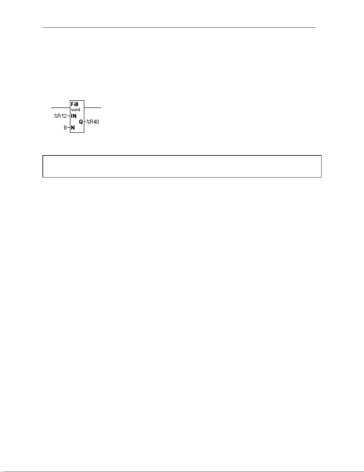
PAGE 60 17 SEP 2002 MAN0313-04
WARNING: If the IN value is a signed numeric constant, it is treated as an unsigned number when the
CH. 2
BLOCK FILL
NOTE: The Block_Fill element operates on 16-bit data only.
This element fills a block of registers with a given value. The IN value can be either an integer constant
or the value contained in another register.
BLOCK FILL
element is configured. For example, if IN is configured as '-1', the value '65535' is used.
Using the above illustration as an example, the registers contain the following before the move operation
is performed:
%R12 1234
%R40 3221
%R41 4632
%R42 65535
%R43 32456
%R44 1
%R45 0
%R46 10
%R47 812
%R48 0
%R49 5
After the element is completed the registers contain:
%R12 1234
%R40 1234
%R41 1234
%R42 1234
%R43 1234
%R44 1234
%R45 1234
%R46 1234
%R47 1234
%R48 0
%R49 5
Page 61
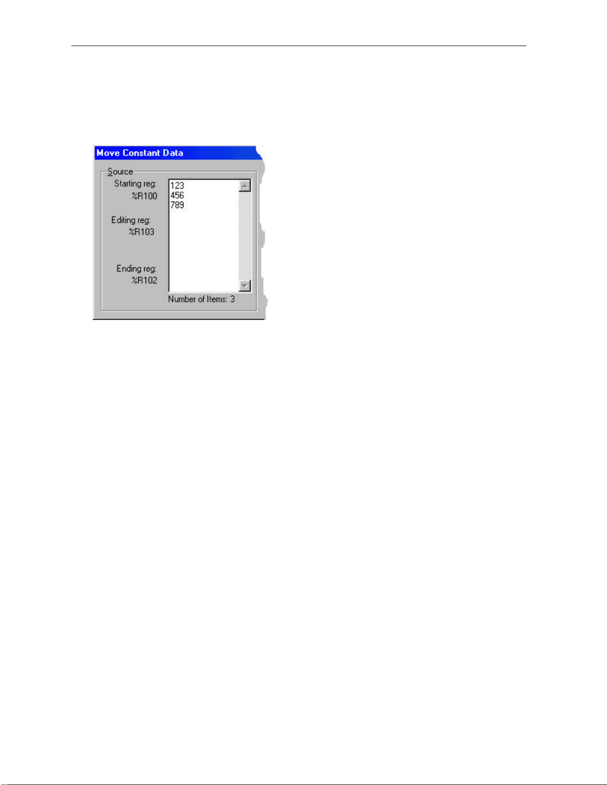
MAN0313-04 17 SEP 2002 PAGE 61
CH. 2
MOVE CONSTANT
The Move Constant Data function allows a table of constants to be loaded into a group of consecutive
controller registers. The table of constants can contain INT, UDINT, DINT, UDINT or REAL types. All
entries in the table mus t be of the same type.
CONST DATA
Assuming the following constant INT table:
NOTE: Constant data can be copied and pasted to/from other Windows application including Microsoft
Excel and Word.
NOTE: REAL numbers less than zero must contain a leading zero (e.g., .999 is valid, 0.999 is valid).
After the element is completed the registers contain:
%R100 123
%R101 456
%R102 789
Page 62
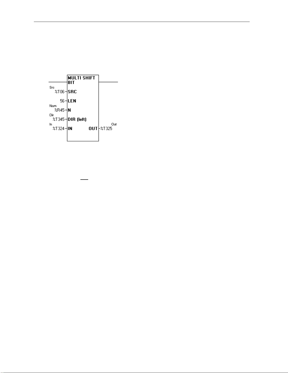
PAGE 62 17 SEP 2002 MAN0313-04
CH. 2
2.13.2 Multi Data Moves
MULTI SHIFT DATA MOVE
This function allows an array of BITS, BYTES, WORDS, and DWORDS to be shifted left or right a
variable numbers of elements.
MULTI SHIFT BIT
a. Power Flow
When the input to this function block is high it completes a shift as specified by the parameters every
scan. This function is not edge sensitive. This function always passes power flow.
b. Multi Shift Move Terminology
SRC - This is the starting BIT, BYTE, WORD or DWORD for the array to be shifted. After the data is
shifted it is stored in the array of data starting at this location. BIT arrays can start at any location (%I1,
%I6, %R1.1, and %R4.7...). BYTE, WORD, and DWORD arrays must start on a WORD boundary (%I1,
%I17, %I33, %R1, and %R2...).
LEN - This is the number of BITS, BYTES, WORDS, or DWORDS in the array. This must be a constant
number from 1 to 32767.
N - This is the number of elements to shift. This can be a constant or a WORD variable.
Page 63
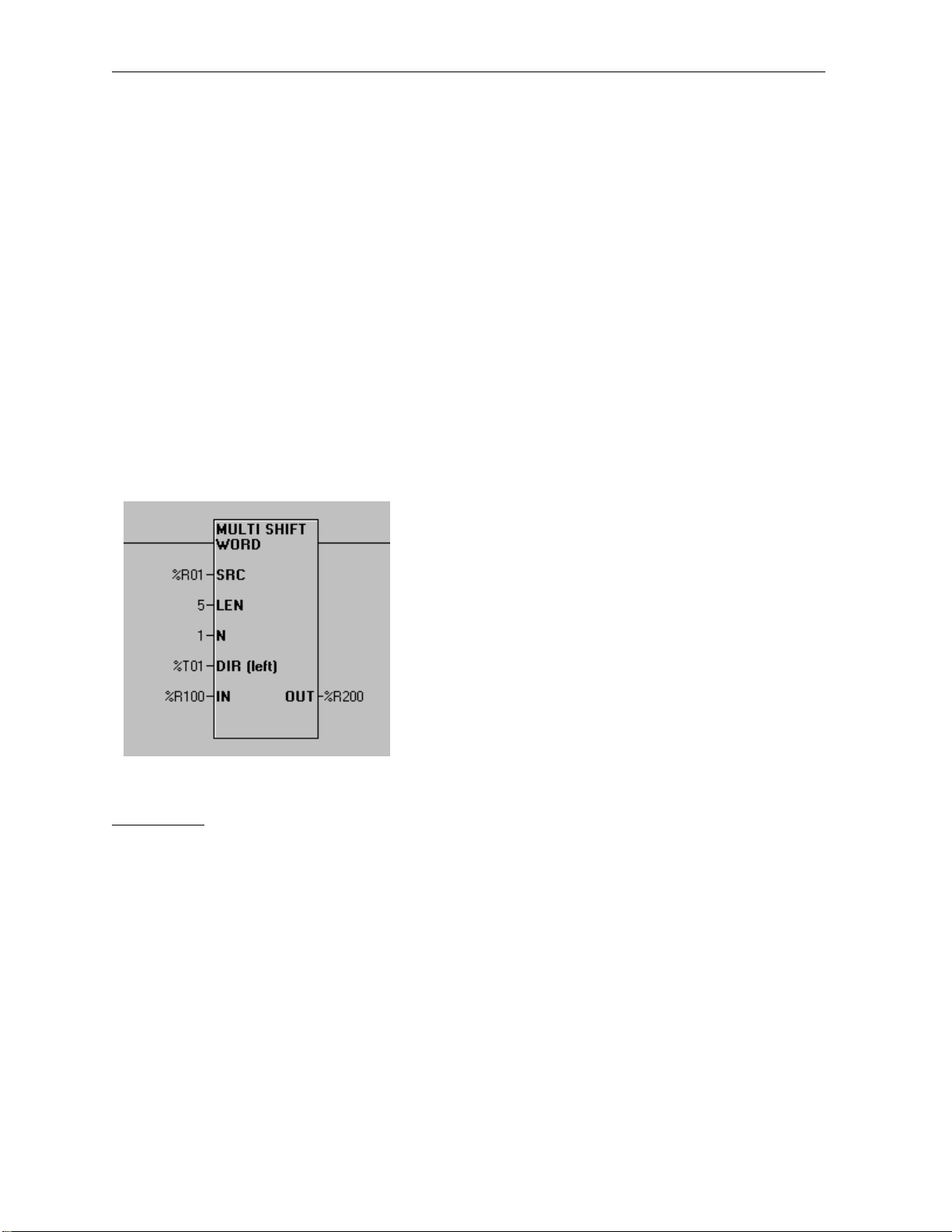
MAN0313-04 17 SEP 2002 PAGE 63
CH. 2
DIR - This is the direction to shift. If this input is high the data is shifted to the left. If this input is low the
data is shifted to the right.
Examples:
BITs Left by 1: %T2 <- %T1 &T3 <- %T2...
BYTEs Left by 1: %R1(high byte) <- %R1(low byte) %R2(low byte) <- %R1(high byte)...
WORDs Left by 1: %R2 <- R1 %R3 <- %R2...
DWORDs Left by 1:%R3, %R4 <- %R1, %R2 %R5, %R6 <-%R3, %R4
BITs Right by 1: %T2 -> %T1 &T3 -> %T2...
BYTEs Right by 1: %R1(high byte) -> %R1(low byte) %R2(low byte) -> %R1(high byte)...
WORDs Right by 1: %R2 -> R1 %R3 -> %R2...
DWORDs Right by 1:%R3, %R4 -> %R1, %R2 %R5, %R6 ->%R3, %R4
IN - This is the BIT, BYTE, WORD, or DWORD to shift into the array.
OUT - This is the last BIT, BYTE, WORD or DWORD shifted out of the array.
c. Examples Multi Shift Word Moves
The graphic below is used with the following examples of Multi-Shift Word Moves.
MULTI SHIFT WORD (Illustrates Example 1, 2, and 3)
EXAMPLE 1:
Start with the registers in the following state:
%R1 1
%R2 2
%R3 3
%R4 4
%R5 5
%T1 TRUE
%R100 123
%R200 0
Page 64

PAGE 64 17 SEP 2002 MAN0313-04
CH. 2
After one scan with power flow to the function high:
%R1 123
%R2 1
%R3 2
%R4 3
%R5 4
%T1 TRUE
%R100 123
%R200 5
After a second scan with power flow to the function high:
%R1 123
%R2 123
%R3 1
%R4 2
%R5 3
%T1 TRUE
%R100 123
%R200 4
Notice the flow of data from the input though the array of WORDS (%R1 to %R5) and finally to the output.
EXAMPLE 2:
Start again with the registers in the following state:
%R1 1
%R2 2
%R3 3
%R4 4
%R5 5
%T1 TRUE
%R100 123
%R200 0
After one scan with power flow high, change the input (%R100) to 456:
%R1 123
%R2 1
%R3 2
%R4 3
%R5 4
%T1 TRUE
%R100 456
%R200 5
After a second scan with power flow to the function high:
%R1 456
%R2 123
%R3 1
%R4 2
%R5 3
%T1 TRUE
%R100 456
%R200 4
Page 65
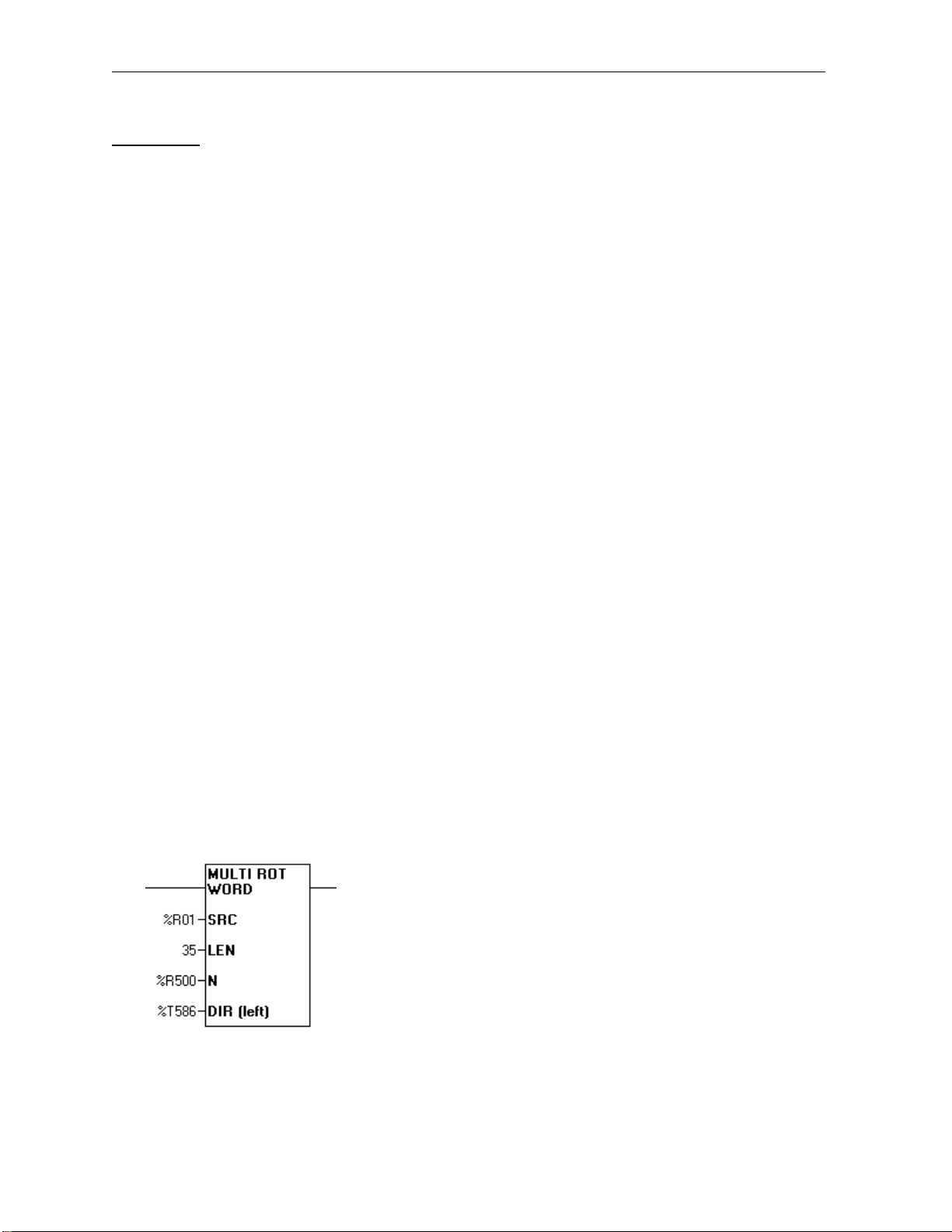
MAN0313-04 17 SEP 2002 PAGE 65
CH. 2
EXAMPLE 3
Start with the registers in the following state (note the DIRECTION is now right):
%R1 1
%R2 2
%R3 3
%R4 4
%R5 5
%T1 FALSE
%R100 123
%R200 0
After one scan with power flow to the function high:
%R1 2
%R2 3
%R3 4
%R4 5
%R5 123
%T1 TRUE
%R100 123
%R200 1
After a second scan with power flow to the function high:
%R1 3
%R2 4
%R3 5
%R4 123
%R5 123
%T1 TRUE
%R100 123
%R200 2
Notice the flow of data from the input, though the array of WORDS (%R5 to %R1) and finally to the
output.
2.13.3 Multi Rotate Data Moves
This function allows an array of BITS, BYTES, WORDS, and DWORDS to be rotated left or right a
variable numbers of elements.
MULTI ROTATE WORD
Page 66
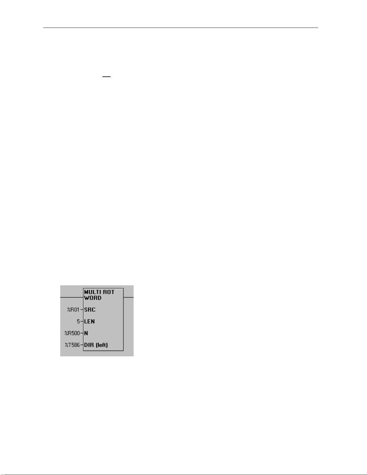
PAGE 66 17 SEP 2002 MAN0313-04
CH. 2
a. Power Flow
When the input to this function block is high it completes a rotate as specified by the parameters every
scan. This function is not edge sensitive. This function always passes power flow.
b. Multi Rotate Data Move Terminology
SRC - This is the starting BIT, BYTE, WORD or DWORD for the array to be rotated. After the data is
rotated it is stored in the array of data starting at this location. BIT arrays can start at any location (%I1,
%I6, %R1.1, %R4.7...). BYTE, WORD, and DWORD arrays must start on a WORD boundary (%I1,
%I17, %I33, %R1, %R2...).
LEN - This is the number of BITS, BYTES, WORDS, or DWORDS in the array. This must be a constant
number from 1 to 32767.
N - This is the number of elements to rotate. This can be a constant or a WORD variable.
DIR - This is the direction to rotate. If this input is high the data is rotated to the left. If this input is low
the data is rotated to the right.
Examples:
BITs Left by 1: %T2 <- %T1 &T3 <- %T2...
BYTEs Left by 1: %R1(high byte) <- %R1(low byte) %R2(low byte) <- %R1(high byte)...
WORDs Left by 1: %R2 <- R1 %R3 <- %R2...
DWORDs Left by 1:%R3, %R4 <- %R1, %R2 %R5, %R6 <-%R3, %R4
BITs Right by 1: %T2 -> %T1 &T3 -> %T2...
BYTEs Right by 1: %R1(high byte) -> %R1(low byte) %R2(low byte) -> %R1(high byte)...
WORDs Right by 1: %R2 -> R1 %R3 -> %R2...
DWORDs Right by 1:%R3, %R4 -> %R1, %R2 %R5, %R6 ->%R3, %R4
c. Examples of Multi Rotate Word Moves
The graphic below is used for the following Multi Rotate Word Moves examples.
MULTI ROTATE WORD
Page 67

MAN0313-04 17 SEP 2002 PAGE 67
CH. 2
Example 1
Start with the registers in the following state:
%R1 1
%R2 2
%R3 3
%R4 4
%R5 5
%T586 TRUE
%R500 1
After one scan with power flow to the function high:
%R1 5
%R2 1
%R3 2
%R4 3
%R5 4
%T586 TRUE
%R500 1
After a second scan with power flow to the function high:
%R1 4
%R2 5
%R3 1
%R4 2
%R5 3
%T586 TRUE
%R500 1
Example 2
Start with the registers in the following state (note the DIRECTION is now right):
%R1 1
%R2 2
%R3 3
%R4 4
%R5 5
%T586 FALSE
%R500 1
After one scan with power flow to the function high:
%R1 2
%R2 3
%R3 4
%R4 5
%R5 1
%T586 FALSE
%R500 1
Page 68

PAGE 68 17 SEP 2002 MAN0313-04
CH. 2
After a second scan with power flow to the function high:
%R1 3
%R2 4
%R3 5
%R4 1
%R5 2
%T586 FALSE
%R500 1
2.14 Set Real Time Clock Element
This function allows the real time clock in the controller to be set from the ladder program. This allows the
clock on several devices to be synchronized over the network, or allow the time to be adjusted based on
a algorythm in ladder.
The input to this function is six consecutive WORD registers. The register should be in the following
format:
Register 1 New Seconds
Register 2 New Minutes
Register 3 New Hours(24 hour format)
Register 4 New Date
Register 5 New Month (1 = January)
Register 6 New Year (4 digit format)
This function passes power if the supplied new time and date are valid. An example of invalid time would
be hour = 50 or month = 100.
The day of the week is automatically calculated and updated in the real time clock (%SR50).
Page 69
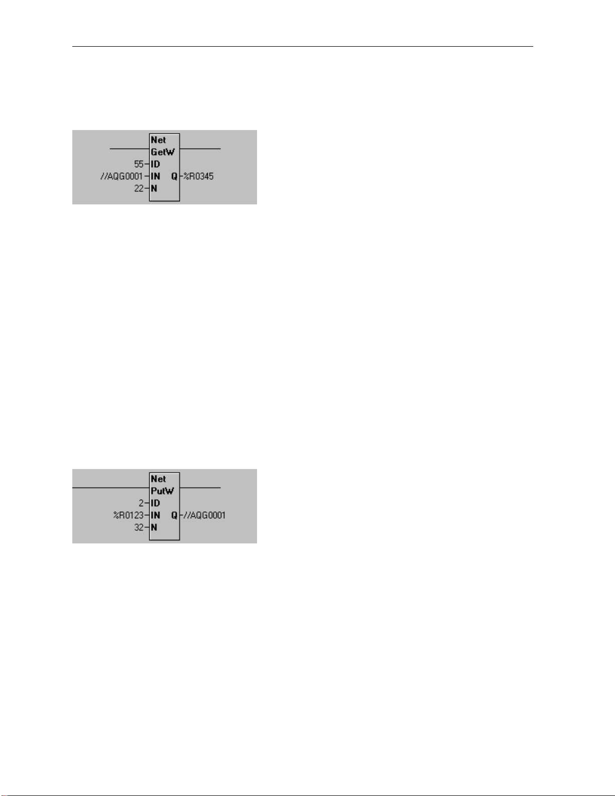
MAN0313-04 17 SEP 2002 PAGE 69
CH. 2
2.15 Network Elements
2.15.1 Net Get Words
This element allows global data from any device on the network to be copied into any set of registers. If
the device defined by the source ID has not transmitted data, this function block will not pass power flow
and will can a request for the data to be sent. Once the request data has been received, power flow from
this function block will turn on.
This function works with CsCAN or DeviceNet networks.
ID - This register or constant defines the source for the global data. If the ID is not valid, the function will
do nothing and will not pass power.
IN - This defines the starting point for the requested global data. This can be a %AQG or %QG register.
Note that %QG registers must be on a word boundary (1, 17, 33...). This is a network register, a register
assigned and produced by the transmitting ID.
N - This defines the number of words to get from the source ID. This has a range of 1 to 32.
Q - This de fines the starting register for the destination of the data. This is a register in the controller.
2.15.2 Net Put Words
This element allows sending global data using multiple networks IDs. This function is not edge sensitive,
every scan that this function is encountered it will copy the data from the source registers attempt to
transmit the data.
This function only works with CsCAN networks.
The function passes power if the ID is legal and in the range defin ed by the network ID and the total
number of ID assigned to that node.
ID - This is a register or constant for the ID to use when transmitting data on the network. It must be in
the range defined by the primary network ID and the total nodes allocated for this target.
IN - This is the starting register for the source data to send on the network. This is a register local to the
controller.
Page 70
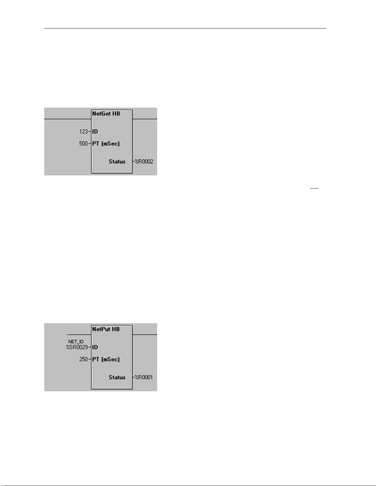
PAGE 70 17 SEP 2002 MAN0313-04
CH. 2
N - This is the number of words to send on the network.
Q - This is the starting register for the destination of the data. Note that %QG registers must be on a
word boundary (1, 17, 33...). This is a network register assigned to the network ID.
2.15.3 Net Get Heartbeat
This function allows the detection of a network heartbeat from another device. This function does not
generate any network traffic.
This function works only with CsCAN networks.
This function will not pass power flow if the ID is not in the legal range or if the device being monitored
does not send a heartbeat message in the timeout defined by PT.
ID - This is a register or constant defining the ID of the device to monitor for a heartbeat.
PT - This is the maximum amount of time to wait for the heartbeat from the monitored device. This
timeout should be greater than the rate the device is sending heartbeat messages. Depending on
network traffic and scan rates the GET timeout should be 10 to 1000 milliseconds greater than the PUT.
This has a range of 1 to 6553 milliseconds.
Status - This register is currently used for internal record keeping. Do not allow other function to write to
this register.
2.15.4 Net Put Heartbeat
This function allows a device to transmit a heartbeat CsCAN message at a given rate to indicate to other
devices it is on-line and operating normally. This function does generate network traffic. The message
generated normally does not affect bandwidth, but if many devices send heartbeat messages frequently it
may cause reduction in bandwidth.
Page 71

MAN0313-04 17 SEP 2002 PAGE 71
CH. 2
This function will not pass power flow if the ID is not in the legal range.
This function works only with CsCAN networks.
ID - This register or constant is usually the primary network ID of the device (%SR29), but can be in the
range defined by the primary network ID and the total number of IDs assigned to this device.
PT - This is how often in milliseconds to send the heartbeat message. This has a range of 1 to 6553.
Status - This register is currently used for internal record keeping. Do not allow other function to write to
this register.
2.16 String Handling Elements
2.16.1 Overview
A string is a succession of characters. Cscape strings are delimited (prefixed and suffixed) by the Single
Quote character ( ' ). Cscape strings can be zero characters in length.
The following are some valid Cscape strings. Note the placement of the Single Quote characters.
'Hot' Length = 3
'' Length = 0
' ' A single SPACE character. Length = 1
Any 8-bit binary value is acceptable in a string not just ASCII characters. However, the usefulness of
non-ASCII characters is limited by the display capabilities of the unit for which they are intended.
2.16.2 Special Characters (String)
Because the Single Quote ( ' ) is used to delimit strings, the Single Quote can not be inserted directly into
a Cscape String. In order to insert a Single Quote, a two-character combination is used. The marker
character is the Dollar Sign $. Using this method, several other useful Special Character combinations
are available.
Combination
$$
$'
$L or $l
$N or $n
$P or $p
Dollar Sign
Single Quote
Line Feed
New Line
Form Feed (page
Printed
Interpretation
feed)
$R or $r
$T or $t
Carriage Return
Tab
The New Line character ($N) provides an implementation -independent means of defining the end of data
for both physical and file I/O. When printed, the effect is that of ending the current line of text and
resuming printing at the beginning of the next line.
Page 72
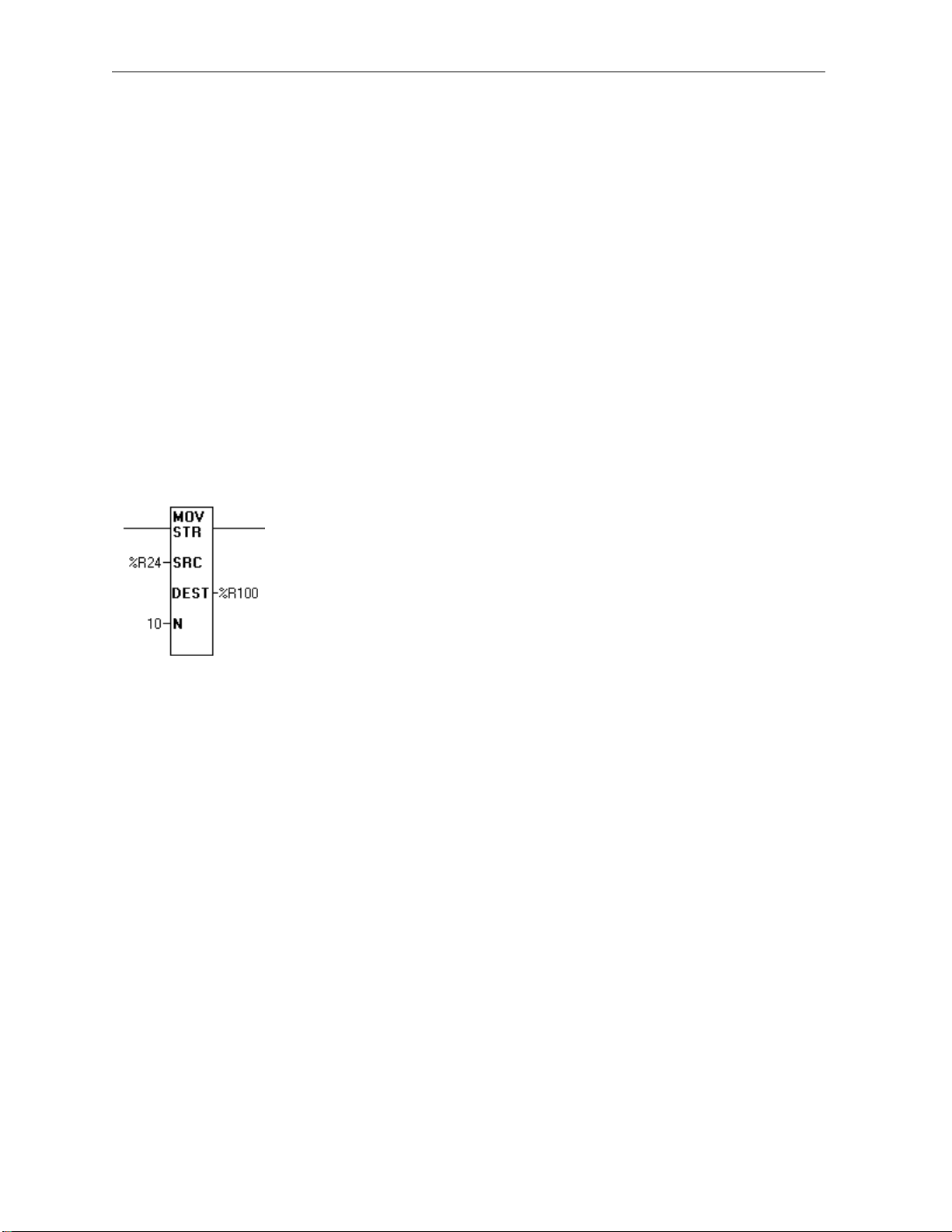
PAGE 72 17 SEP 2002 MAN0313-04
CH. 2
Hexadecimal Numbers
Hexadecimal numbers are also accepted. Hexadecimal number can be entered by using the Dollar Sign
followed by two hexadecimal characters:
Combination Printed Interpretation
$0D
$0D$0A
$00
$FF
Carriage return (same as $R)
CR/LF sequence (same as $R$L)
Null characters
Binary value 255
A hexadecimal number must contain exactly two (2) characters. Possible characters are 0- 9, A- F, and a-
f. The conversion is not case sensitive.
Hexadecimal number must be exactly two characters. If the number can be represented with one
hexadecimal character (i.e., $a), the string must contain a leading 0 (i.e.: $0a).
String Move Element
MOVE STRING
When power is applied to this element, it moves the programmed number of characters from SOURCE to
DESTINATION.
SOURCE can be either a Register Type and Offset reference, or a string constant. String constants must
be delimited with the Single Quote character ( ' ). (For example, “This is a test.”
DESTINATION must be a Register Type and Offset Reference.
N is the number of character to move, and must be a decimal constant.
If SOURCE is a string constant (i.e., the first character is a Single Quote), then the Number of
Characters entry box is disabled, and contains the count of the number of characters typed in. Note that
a hexadecimal sequence (‘$0A’) appearing in a string constant is counted as a single character.
Page 73
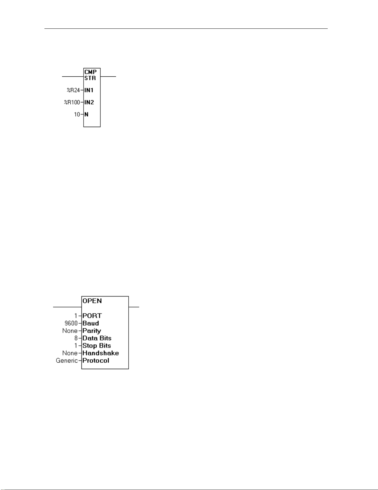
MAN0313-04 17 SEP 2002 PAGE 73
CH. 2
String Compare Element
String Compare
When power is applied to this element, it compares the programmed number of characters from IN1 with
any characters appearing at IN2. If the comparison is TRUE (the two strings are equal), then power flow
through the elements is TRUE.
IN1 may be either a Register Type and Offset reference, or a string constant. String constants must be
delimited with the Single Quote character ( ' ); for example, “This is a test.”
IN2 must be a Register Type and Offset Reference.
N is the number of character to compare and must be a decimal constant. If IN1 is a string constant (i.e.,
the first character is a Single Quote), then the Number of Characters entry box is disabled, and contains
the count of the number of characters typed in. Note that a hexadecimal sequence ('$0A') appearing in a
string constant is counted as a single character.
2.17 Communication Elements
2.17.1 Configuring Serial Port Elements (Communication)
Open Comm Port
Serial Port Open
The Open Port element creates a channel to the desired comm port. The operational parameters (baud
rate, etc) are also set by this element. The channel remains open until closed by the Close Port element
or the controller is taken out of RUN mode.
The configuration dialog consists of a number of drop -down selection lists. Make the selection of the
comm port's operational parameters from these lists.
Page 74
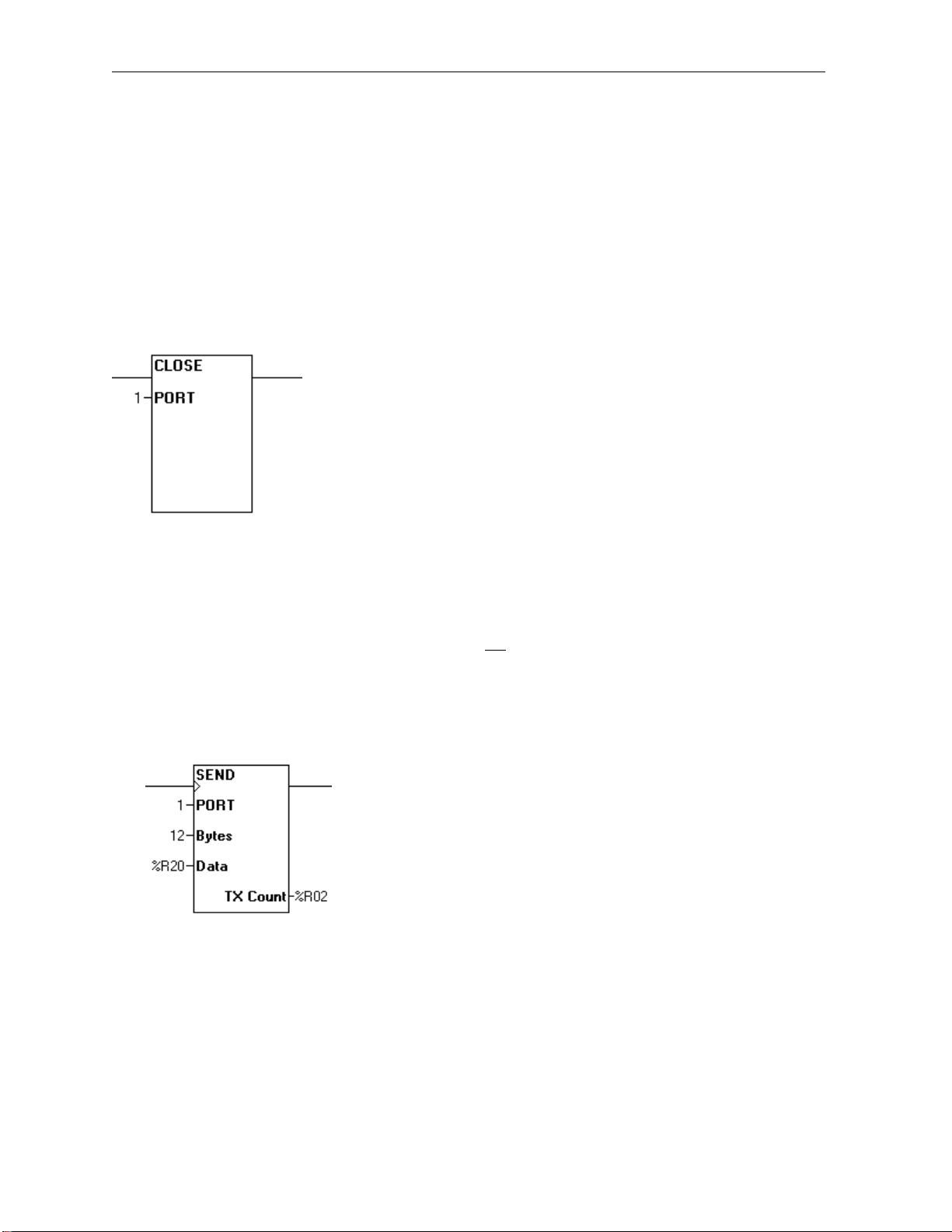
PAGE 74 17 SEP 2002 MAN0313-04
CH. 2
NOTE: In the current release of the OCS hardware there is only one comm port available, Port 1.
Power flow through the element is TRUE if the element completes successfully or if the port is already
open. If one attempts to open a port that does not exist, power flow through the element is FALSE.
The selected port can not be used for programming using the CsCAN protocol if it has been otherwise
opened by this element. OCS units with only one comm po rt can still be programmed by using a Pass
Through Connection from another unit.
Close Comm Port
SERIAL PORT CLOSE
This element closes the channel to the selected port. There are no operational parameters except the
Port Number. This entry must be a decimal constant.
Power flow through the element is TRUE if the element completes successfully or if the port is already
closed. If an attempt is made to close a port that does not exist, power flow through the element is FALSE
If the selected port had been previously used as a CsCAN programming port, that function is again
available.
Comm Port Transmit
SERIAL PORT SEND
If the port has been successfully opened, this element sends a specified number of bytes to the internal
transmit buffer for the selected comm port.
PORT is the comm port previously open by the ladder program.
NOTE: In the current release, the only available comm port is Port 1.
Page 75
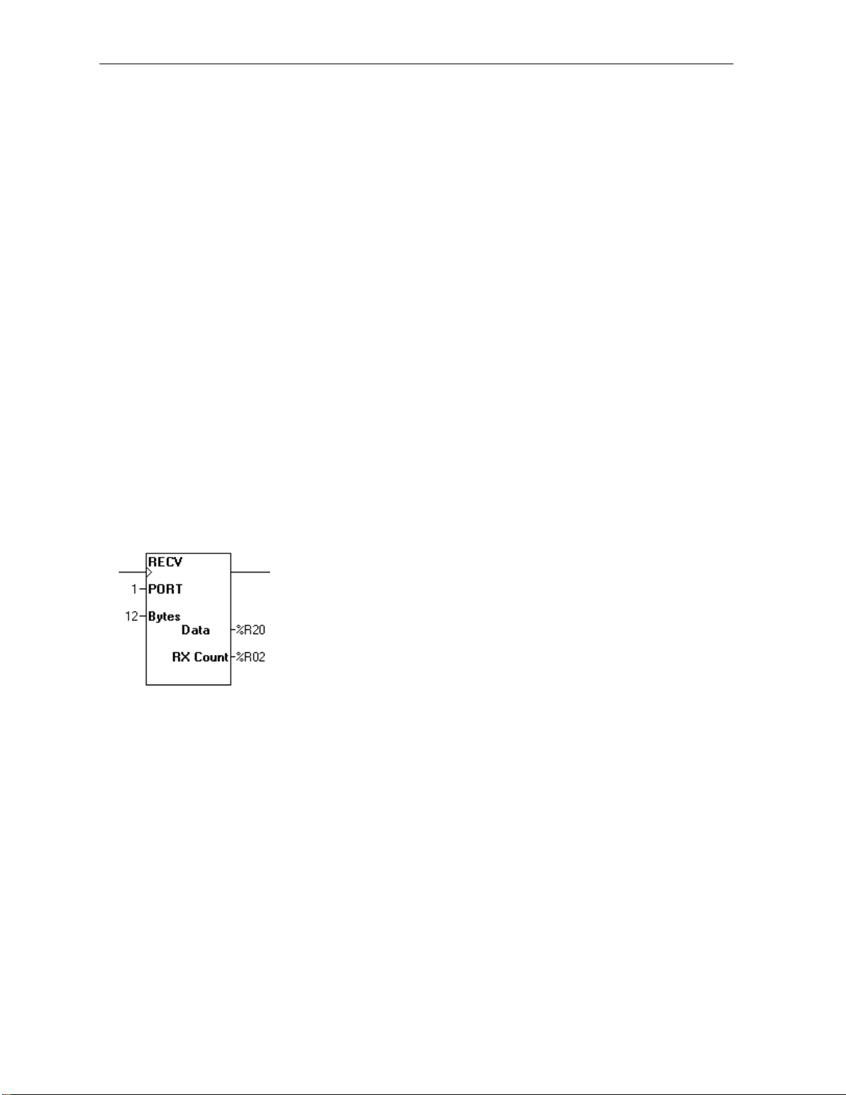
MAN0313-04 17 SEP 2002 PAGE 75
CH. 2
BYTES may be specified as either a Register Type and Offset reference or as a decimal constant. This
value indicates the number of bytes to be transmitted.
DATA is the address of the data to be sent. This must be specified as a Register Type and Offset
reference.
TX COUNT contains the actual number of bytes transferred to the port's internal buffer (or -1 when the
function is not. This location must be specified as a register Type and Offset reference.
When power is applied to the element, the TX Count register contains the number of characters actually
transferred to the comm port transmit buffer. If power is not applied to the element, this register contains 1 (negative one).
Power flow through the element is FALSE until the requested number of characters have been
transferred to the comm port transmit buffer (at which time the power flow is TRUE). It is possible that the
element can not transfer all data in one program scan time.
If the port is not open, the Transmit Element does nothing, and power flow through the element is FALSE.
If the value contained in BYTES is greater then 255, the element does nothing and power flow through
the element is FALSE.
The number of bytes can be either a Register Type and Offset references or a decimal constant. The
maximum acceptable value is 255 bytes. When using a Register Type and Offset address, if the register
contains a value less than 0 (zero) or greater than 255, the element does nothing, and power flow through
the element is FALSE.
Comm Port Receive
Serial Port Receive
If the port has been successfully opened, this element receives a specified number of bytes from the
selected comm port.
PORT is the comm port previously opened by the ladder program.
NOTE: In the current release, the only available comm port is Port 1.
BYTES can be specified as either a Register Type and Offset reference or as a decimal constant. This
value indicates the maximum number of bytes to be received.
DATA is the address where the received data is to be stored. This must be specified as a Register Type
and Offset reference.
RX COUNT contains the number of bytes to be copied from the port's internal buffer to the registers at
DATA (or -1 when the function is not.)
I
Page 76
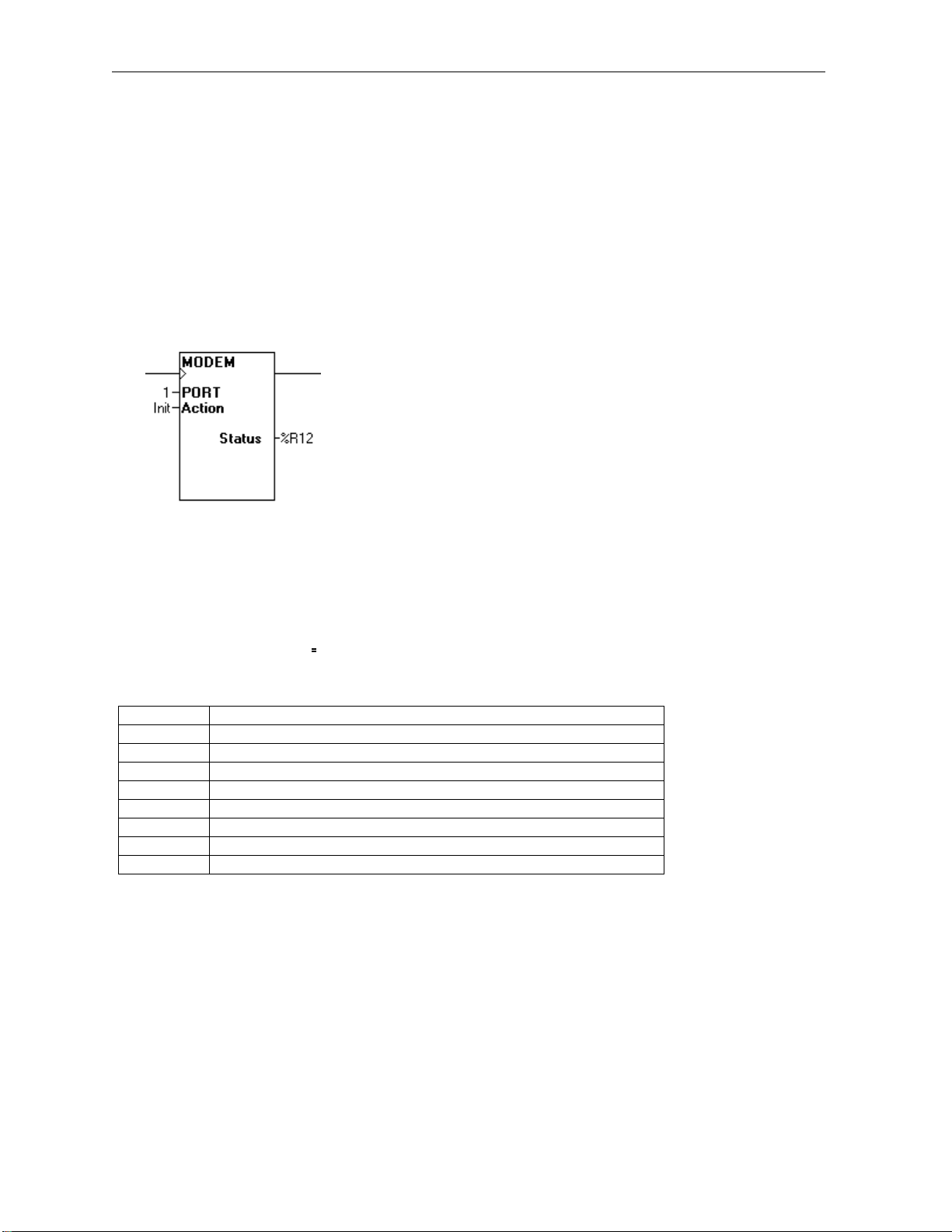
PAGE 76 17 SEP 2002 MAN0313-04
CH. 2
f the port is not opened the Receive Element does nothing, and power flow through the element is
FALSE.
Power flow through the element is FALSE until the requested number of characters has been received
from the comm port buffer (at which time the power flow will be TRUE). It is possible that the element can
not transfer all data in one program scan time, especially at slower baud rates.
The BYTES can be a Register Type and Offset references. The maximum acceptable value is 255
bytes. When using a Register Type and Offset address, if the register contains a value less than 0 (zero)
or greater than 255, the element does nothing, and power flow through the element is FALSE.
MODEM CONTROL
Modem Control
This element allows the OCS to control an attached modem. Port Number is the COMM port to which the
modem is attached.
NOTE: In the current release, the only available comm port is Port 1.
Status is the Type and Offset of a WORD (16-bit) register used to hold the results of the element.
The status can take on the following values while operating:
Value Status
0 The modem completed the operation successfully
1 The modem successfully connected
2 The modem detected an incoming ring
3 The modem lost carrier or did not receive a carrier on a dial
4 The modem indicated an error (check dial or init string)
-1 The function is not active
-2 The function has started, but not completed an operation
-3 The command timed-out (modem did not respond)
Action is the action to be taken. From the drop down list select one of the following:
INITIALIZE - Send the specified Initialization String to the modem.
AUTO DIAL - Cause the modem to dial, given the specified phone number and method (tone or pulse).
AUTO ANSWER ON - Turns ON the modem's Auto-Answer features (if available) and sets the specified
number of rings.
Once a modem connection is made using AUTO DIAL or AUTO ANSWER, the serial send, receive,
Modbus slave and Modbus master function blocks can be used to exchange data with a remote location.
If remote CsCAN communications is desired after the modem connection is established, the serial port
can be closed to switch back to CsCAN mode.
Page 77
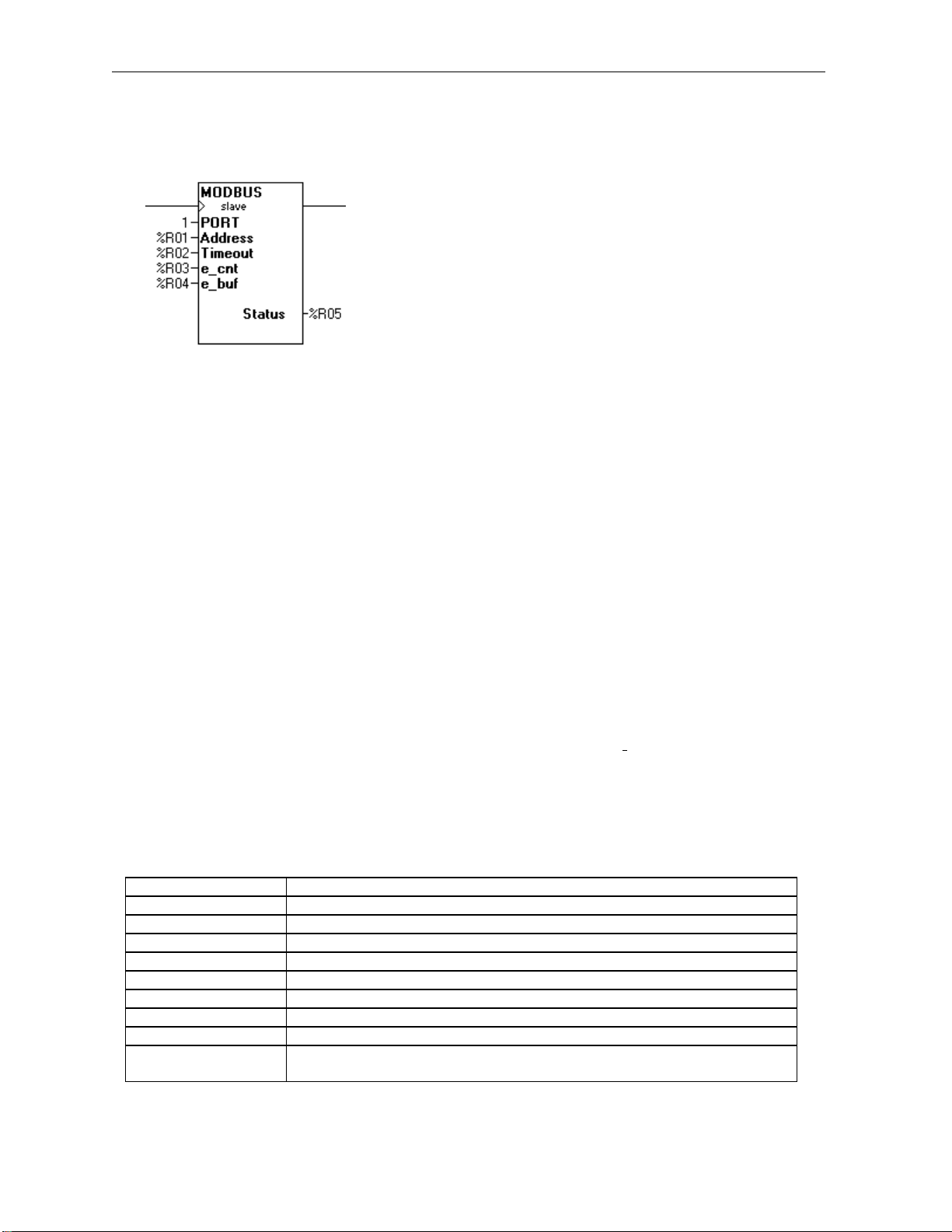
MAN0313-04 17 SEP 2002 PAGE 77
CH. 2
MODBUS SLAVE
Modbus Slave
PORT is the comm port previously opened by the ladder program with Protocol set to Modbus ASCII or
Modbus RTU.
NOTE: In the current release, the only available comm port is Port 1.
ADDRESS can be specified as either a Register Type and Offset reference or as a decimal
constant(with a range of 1 to 247). This specifies the Modbus address the controller uses to respond to
Modbus request.
Timeout can be specified as either a Register Type and Offset reference or as a decimal constant (with
a range of 0 to 1023). This specifies the amount of time that passes between request from the master
before the in -activity timeout bit is set in the status word. This parameter is in terms of 100 milliseconds
(i.e., 100 = 10.0 Sec).
e_cnt (Required only if Exception Message support is enabled) is specified as a Register Type and
Offsetreference. This contains the number of bytes in the Message Data buffer to send. Transition from
zero to a non-zero value triggers the transmission of one Exception Message.
e_buf (Required only if Exception Message support is enabled) is specified as a Register Type and
Offset reference. This is the first register number of an array, which contains the Exception Message
(first message byte is contained in referenced word register low value byte)
STATUS is the Type and Offset reference of a WORD (16-bit) register used to hold the results of the
element.
Status bit assignment:
Bit Number Status
1 Inactivity Timeout
4 Valid message received (toggles)
5 Parity error (single pass)
6 Frame Error (s ingle pass)
7 Overrun error (single pass)
8 Crc/Checksum error (single pass)
9 Exception message send (reset when e_cnt = 0)
10 Exception message exceeds send buffer size (reset when e_cnt = 0)
11 Attempt to send exception message when transmit busy (reset when
e_cnt = 0)
Page 78
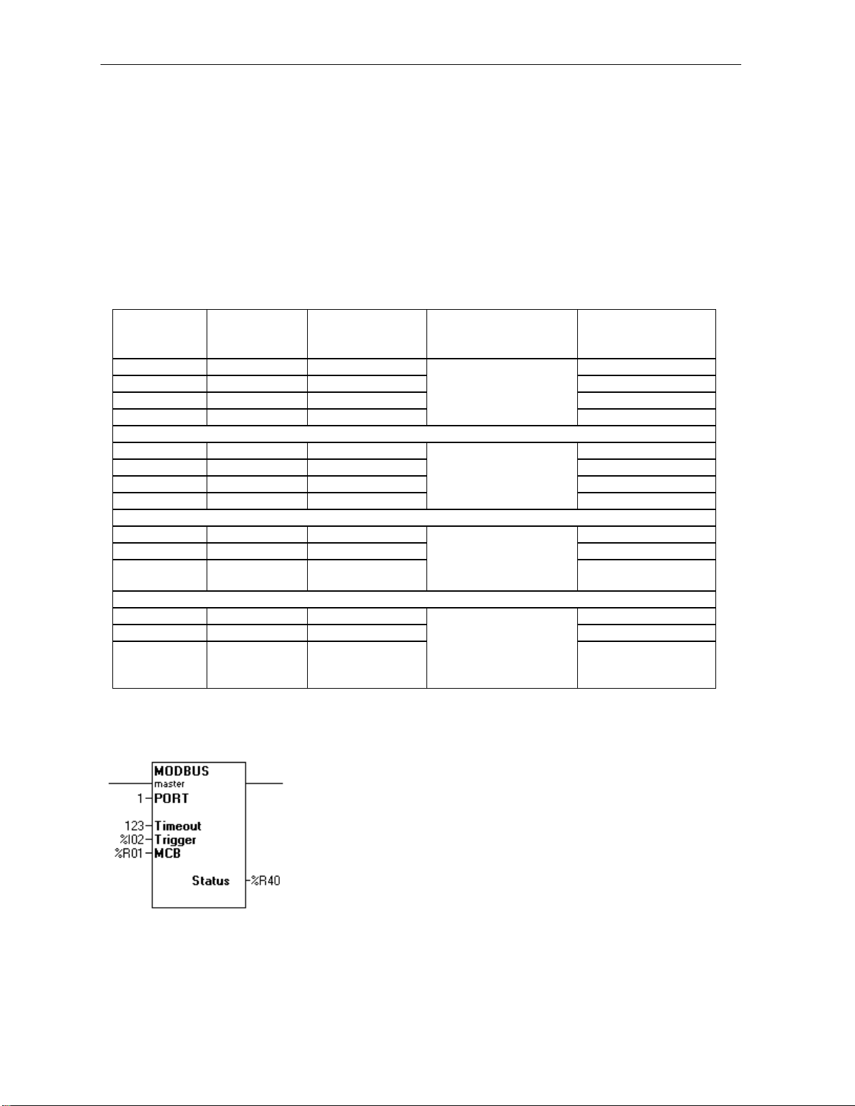
PAGE 78 17 SEP 2002 MAN0313-04
CH. 2
Master Mapping
To access a controller’s point over Modbus, the master must be configured as to the point’s type and
offset. This is usually accomplished with one of two methods. The first method uses the traditional
addressing scheme where the high digit represents the point’s type and the lower digits represent the
point’s offset (starting with point 1). Since only four types can be represented in this manner, the Modbus
function packs several controller data tables into a single point type array.
The Traditional RTU Reference column below specifies the starting address of each controller table. The
second method requires the master to be configured with the specific Modbus command and offset. The
supported Modbus commands and the associated offset are also illustrated in the following table.
Controller
Reference
%I1 2048 10001 00000
%IG1 256 13001 03000
%S1 256 14001 04000
%K1 256 15001
%Q1 2048 00001 00000
%M1 2048 03001 03000
%T1 2048 06001 06000
%QG1 256 09001
%AI1 512 30001 00000
%AIG1 32 33001 03000
%SR1 32 34001
%AQ1 512 40001 00000
%R1 2048 43001 03000
%AQG1 32 46001
MODBUS MASTER
Modbus Master
PORT is the comm port previously open by the ladder program with Protocol set to Modbus ASCII or
Modbus RTU.
Maximum
Range
Traditional
Modbus
Reference
Modbus
Command(s)
Read Input Status (2)
Read Coil Status (1)
Force Coil (5)
Force Multiple Coils
(15)
Read Input Register
(4)
Read Holding
Register (3)
Load Register (6)
Load Multiple
Registers (16)
Modbus
Offset
05000
09000
04000
06000
Page 79

MAN0313-04 17 SEP 2002 PAGE 79
CH. 2
NOTE: In the current release, the only available comm port is Port 1.
Timeout may be specified as either a Register Type and Offset reference, or as a decimal constant(with
a range of 0 to 1023). This specifies the amount of time that is allowed between a Modbus command and
its response. This parameter is in terms of 100 milliseconds (i.e., 100 = 10.0 Sec).
Trigger -is specified as a bit Register Type and Offset reference. When this bit goes from an off to on
transition, the block transmits the Modbus message defined by the message control block (MCB). When
this input is low, the status word is cleared.
MCB (Message Control Block) - is specified as a Register Type and Offset reference. This register is
the first of six (6) registers that contain the control information for this block
Word 1 Slave ID - value from 1 to 247 indicating the device to receive the message
Word 2 Modbus Command - Modbus command to send to the slave (see supported commands)
Word 3 Slave Offset - Starting point in the Modbus slave for data to read or write
Word 4 Data Length - Amount of data to read or write
Word 5 Controller Reference Type - Enumerated controller register type
(see register type enumeration)
Word 6 Controller Reference Offset - Controller register number -1
The following example reads 32 bits of data starting with bit 17,
from slave ID 34, and placed the data in the controller registers starting with %R425:
Word 1 = 34 (Slave ID is 34)
Word 2 = 1 (Modbus command #1 = Read Coil Status)
Word 3 = 16 (Start with the 16th bit)
Word 4 = 32 (Read 32 bits)
Word 5 = 8 (Destination reference type is %R
Word 6 = 424 (Destination offset is 424 [425-1])
STATUS is the Type and Offset reference of a WORD (16-bit) register used to hold the results of the
element.
Status bit assignment:
Bit Number Status
1 Request Succeeded (OK)
2 Request Failed (See additional errors below)
3 ID out of range
4 Length exceeds Modbus frame
5 Command not supported
6 Invalid controller reference
7 Reserved
8 Reserved
9 Timeout Expired
10 Frame or parity error
11 Invalid checksum / crc from slave
12 Invalid format from slave
13 Slave rejected the command
14 Slave rejected the address
15 Slave rejected the data
16 Slave device error
Page 80

PAGE 80 17 SEP 2002 MAN0313-04
CH. 2
This function passes power flow if the associated port is opened and ready for communications.
2.18 Special Elements
2.18.1 Overview
Special Elements are those which have a functions which are outside the classifications of "normal"
ladder logic elements. They include the Stepper Motor Module Configurator and PID Functions.
2.18.2 Stepper Move Element
a. General
The Stepper Move element provides the necessary interface between Cscape and the STP100 Single
Axis Stepper Controller SmartStack module.
The STP100 module requires either seven (7) or fourteen (14) cons ecutive Analog Output (%AQ)
registers. To program the STP100 module, appropriate data must be moved into the assigned %AQ
registers, typically using seven or 14 Move Word elements.
The purpose of the Stepper Move element is to act as a gathering point to organize information from
different points in the ladder program and transfer this data to the STP100 module with one instruction.
Additionally, the Stepper Move element provides a built in Stepper Motion Calculator that can calculate a
Movement Profile graph based on user-selected values.
b. Configuration of the Stepper
NOTE: Verify the SmartStack module configuration before completing the Element Configuration.
The various entri es must be completed by the programmer. Values can be entered as numeric constants
Register Type and Offset, or registers can be referenced by Name.
INDEXED MOVE -- Check this box to enable the Indexed Move features of this element. The SmartStack
module must also be configured to produce Indexed Moves. If Indexed Move is enabled, the element
requires seven (7) additional registers (14 total).
STEPPER STARTING %AQ -- This contains the address of the first %AQ register assigned to the Stepper
SmartStack module. This information can be taken from the Stepper Module SmartStack Configuration.
DESTINATION POSITION -- This is a 32-bit register. This register contains the position where the move
is to end. Values range is -8,388,608 to +8,388,607
VELOCITY RES OLUTION -- This is a 16-bit register. Values range from 20 to 65535.
BASE VELOCITY -- This is a 16-bit register. Values range from 1 to 8190.
RUNNING VELOCITY -- This is a 16-bit register. Values range from 2 to 8191.
ACCELERATION TIME -- This is a 16-bit register. Times are listed in milliseconds (mS). Values range
from 1 to 27300.
DECELERATION TIME -- This is a 16-bit register. Times are listed in milliseconds (mS). Values range
from 0 to 27300.
Page 81
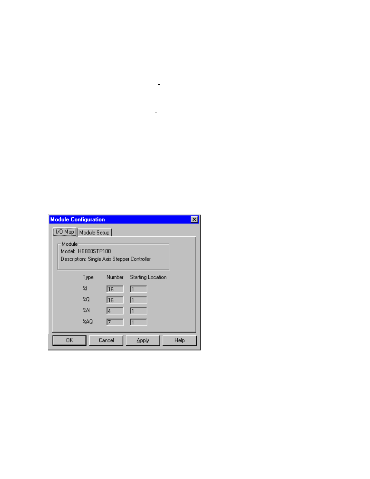
MAN0313-04 17 SEP 2002 PAGE 81
CH. 2
The following registers are used only for Index Move operations:
INDEX DESTINATION POSITION -- This is a 32-bit register.
INDEX DECELERATION -- This is a 16-bit register.
INDEX WINDOW OPEN -- This is a 32-bit register.
INDEX WINDOW CLOSED -- This is a 32- register.
c. Operation
In operation, the Stepper Element gathers the indicated information and writes all values as a group to
the Stepper Controller SmartStack Module. [Technically, the actual write operation does not take place
until the next I/O cycle.] This is a great convenience as to do this the normal way would require six or ten
individual elements. The Stepper Move instruction requires only one element.
The registers assigned to the Stepper Controller SmartStack Module are assigned by default when the
controller is configured. The exact position of the module in the %I, %Q, %AI, and %AQ spaces is
determined by the number of SmartStack modules attached to this controller, and the physical position of
the HE800STP100 module within the stack. This is a typical setup based on the STP100 being the first
(or only) SmartStack module, and indexing is not selected:
Stepper Config
Note the STARTING LOCATION indicated for this module, in particular those for %AQ. This information is
used in the configuration screen. In this example, the Stepper Controller lives at address %AQ01 and
requires seven (7) consecutive registers. This information belongs in the Stepper Starting %AQ box
of the element configuration screen.
NOTE: If the module and the element are configured to accept Indexed Moves, the element requires
fourteen (14) consecutive %AQ registers.
Page 82

PAGE 82 17 SEP 2002 MAN0313-04
CH. 2
First ensure that the SmartStack module is free to operate by checking the Status Bits, %I1 to %I16. If
any Error Bit is set, the source of the error must be cleared, and the CLEAR ERRORS command issued.
Condition of the Status Bits depends on the previous command. Do not issue a new command (except
the IMMEDIATE STOP or DECELERATE AND STOP command) until the previous command has
completed.
When this element receives power, the values from the configured constants or registers are loaded into
the STP100, preparing it for the next command. [Technically, the actual write operation does not take
place until the next I/O cycle]
NOTE: DO NOT execute the Stepper Move element until the previous command is complete.
Commands are issued by setting the appropriate command bit in the Stepper Modules %Q address
space after the Stepper Move element has completed.
2.18.3 Stepcalc Motion Profile Calculator
Cscape contains a built in Motion Profile Calculator.
NOTE: Use of the Motion Profile Calculator does not effect the OCS registers.
In operation, one can enter experimental values into the Motion Profile Calculator. The calculator then
determines whethe r or not the values are valid for the Stepper Move element, and if they are, then key
values are presented to see if the move is within the capabilities of the stepper motor hardware. Finally,
one can view a graph or profile of the intended move.
Velocity Resolution, Base Velocity, Running Velocity, Acceleration Time, and
Deceleration Time are all values that are intended to be placed into the corresponding Stepper
Controller Registers through the Stepper Move element. In order for StepCalc to operate, these values
must be entered.
The Number of Pulses entry is optional. This value is used if a trapezoidal move is to be profiled.
Possible values for this entry are in the range 0 to +16777215. Entering 0 (zero) is used to profile JOG or
TRIANGULAR moves .
The other entries are adjusted and the profile recalculated. The maximum possible settings are:
VELOCITY RESOLUTION -- Values range from 20 to 65535.
BASE VELOCITY -- Values range from 1 to 8190.
RUNNING VELOCITY -- Values range from 2 to 8191. Value must be greater than BASE VELOCITY.
ACCELERATION TIME -- Values range from 1 to 27300.
DECELERATION TIME -- Values range from 0 to 27300.
These values may be more severely limited by the other values entered into the calculator. StepCalc
issues a warning if a value is exceeded.
Once acceptable value are entered, press the UPDATE button. The value displayed in the dialog is
recalculated and displayed. To see the resulting Motion Profile, press the Calc/Graph button.
Page 83

MAN0313-04 17 SEP 2002 PAGE 83
CH. 2
2.18.4 PID Elements
a. General
Cscape provides two (2) PID (Proportional / Integral / Derivative) elements: Independent and ISA. These
two elements differ only in how the proportional gain (Kp) component effects final outcome. These are the
two equations used:
Independent PID CVout = (Kp * Error) + (Ki * Error * dt) + (Kd * Derivative) + CVBias
ISA PID
CVout = Kp * (Error + (Error * dt / Ti) + (Td * Derivative)) + CVBias
Where:
dt = Internal elapsed time clock - previous elapsed time clock
Derivative = (Error - previous Error)/dt
- -or--
Derivative = (pv - previous PV)/dt
Ti = Integral time
Td = Derivative time
[User selectable during configuration].
From these equation, one can see that in the Independent PID the Kp value is used alone while in the ISA
PID, the Kp value is used to factor both the Ki and Kd values.
The Independent PID is the standard function, but the ISA PID is a bit easier to tune.
Page 84

PAGE 84 17 SEP 2002 MAN0313-04
CH. 2
b. PID Register Usage
Either PID element requires an array of fifteen (15) WORD (16-bit) registers. These will presumably be of
type %R. This is called the Reference Array.
Offset Parameter Units Range Description
0 Sample
Period
1 Dead Band + PV Counts 0 to 32000 Defines the Upper and Lower Dead Band
2 Dead Band - PV Counts 0 to 32000
3 Proportional
Gain
(Kp)
4 Derivative
Gain
(Kd)
5 Integral Rate
(Ki)
6 CV Bias CV Counts -32000 to
7 CV Upper
Clamp
8 CV Lower
Clamp
9 Minimum Slew
Each PID element must use a distinctly separate Ref erence Array, even if the values are identical to an
exiting PID element. There can be no overlapping of PID elements.
Time
10 Config Word N/A N/A Internal Use - Do not modify this value
11 Manual
Command
12 Internal SP Used by
13 Internal PV Used by
14 Internal CV Used by
10 mS 0 to 65535 The shortest time, in 10mS increments,
allowed between PID solutions
limits in terms of PV counts.
Set both to 0 (zero) if no dead band is
required.
Both should be set to 0 (zero) until the PID
is tuned. A Dead Band might then be
necessary to prevent small changes in CV
values due to slight variations in error.
Percent 0 to 327.67% Sets the Proportional Gain (Kp) factor in
terms of percent. 100 sets unity gain (gain
of 1
10 mS 0 to 327.67
seconds
1000
second
CV Counts -32000 to
CV Counts -32000 to
Seconds of
full travel
CV Counts Tracks CV in
OCS
OCS
OCS
0 to 32.767
repeats per
second
+32000
+32000
+32000
0 to 32000
seconds to
move 32000
CV counts
Auto mode;
sets CV in
Manual Mode.
N/A Tracks SP in
N/A Tracks PV in
N/A Tracks CV out
Entered as a time with a resolution of 10
mS.
In the PID equation this has the effect: Kd
* delta Error / dt
Entered as a number of repeats per second
-- effectively the integration rate. In the PID
equation this has the effect: Ki * Error
* dt
Number of CV counts added to the output
before the rate and amplitude clamps
Number of CV Counts that represent the
highest and lowest value for CV. CV Upper
Clamp must be more positive the CV Lower
Clamp
Determines how fast the CV valu e can
change
In the Automatic mode this register tracks
the CV value.
In the Manual Mode, this register contains
the value that is output to the CV within the
clamp and slew limits.
Page 85

MAN0313-04 17 SEP 2002 PAGE 85
CH. 2
Registers at offset 0 through 9 must be configured before the PID element is used. This is most easily
done using the Tune features of the Cscape PID Element Configuration. These registers can, however,
be manipulate by the ladder program as well.
c. Independent PID Element / ISA PID Element
PID Element With and Without Auto Tuning
The element is configured to accept five (5) external variables -- two word (16-bit) values and three (3)
binary (1 bit) values. The element outputs one word (16-bit) variable and one single-bit variable.
The element uses an array of fifteen (15) word (16-bit) registers, presumably type %R. This is known as
the Reference Array (see below).
In operation, when the element receives power, and the Manual Input does not receive power, the
element is placed in the Automatic Mode. The element first determines if its sample time period has
elapsed. If the time period has elapsed, the PID algorithm is solved and the Control Variable (CV) is
updated.
If power is applied to the element and power is also applied to the Manual input, the element operates in
the Manual Mode. The Control Variable (CV) is updated using the value in the Manual Command
Parameter in the reference array. If the UP or DOWN inputs are also active, the CV count is incremented
or decremented by one CV count on every PID solution.
In either manual or automatic modes, the CV Output value is limited by both the CV Clamp Value and the
CV Slew Limit value. If the Internal CV value exceeds either clamp value or the rate of change of the
Internal CV exceeds the Slew Limit, the value of CV Output is clamped at the limit. CV Output moves
away from the clamp value at such time as the Internal CV values drops below the clamp or the slew rate
drops below the CV Slew Rate limit. This provides an anti-windup protection and bumpless transfer
between automatic and manual modes.
Page 86
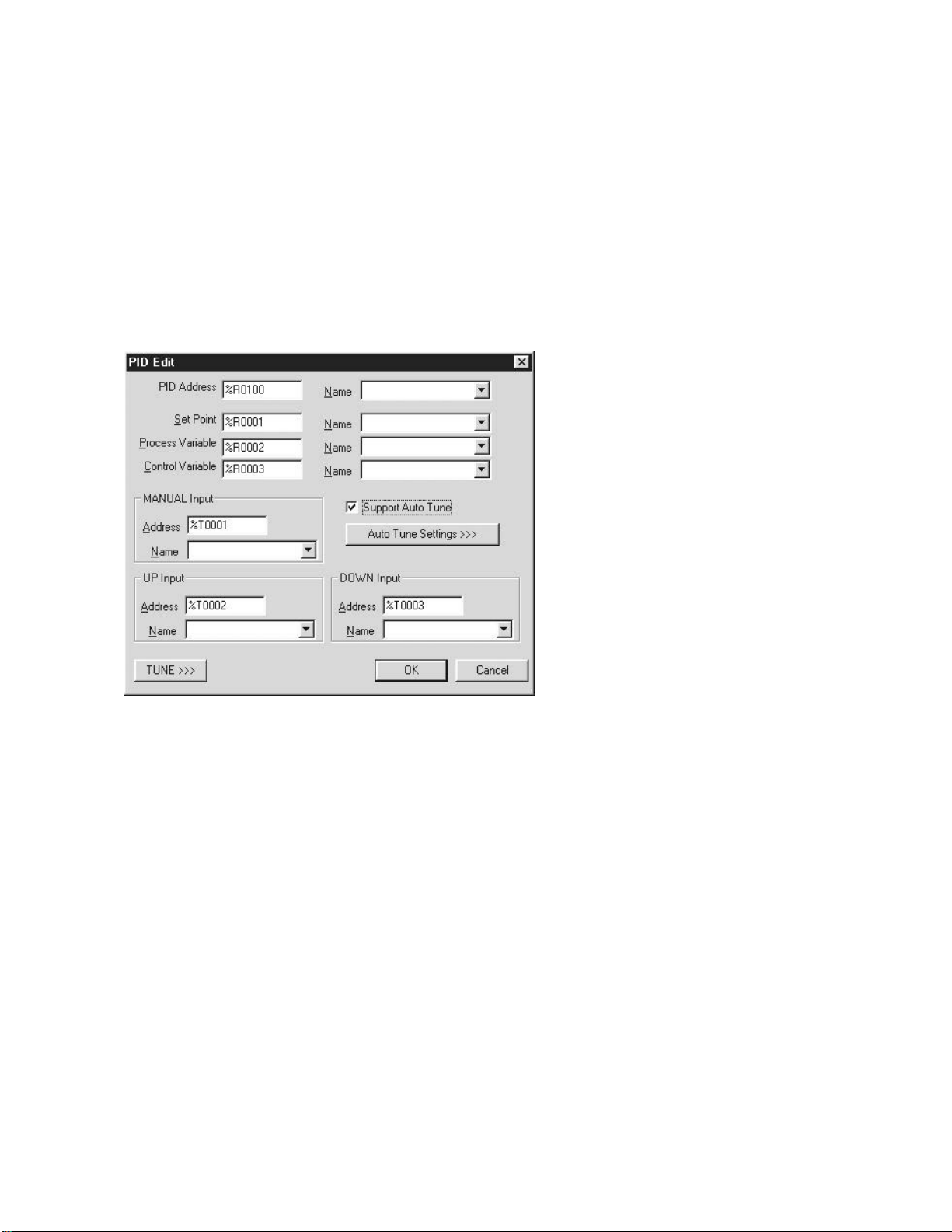
PAGE 86 17 SEP 2002 MAN0313-04
CH. 2
If the element receives power, it solves the PID equation only if the sample time period has been
exceeded. Setting the Sample Time Period to 0 indicates that the equation is to be solved every time the
element is enabled, but in no case the element executes faster than once every 10 milliseconds. For
example, if the OCS scan time is 9 milliseconds, and Sample Time Period is set to 0 (zero), the element
executes once every other scan, or 18 mS. The element can not execute in the first scan, because the
10 millisecond minimum limit has not been met. The element can not again execute until the next scan, 9
milliseconds later.
d. Configuration of PID
The elements are configured from the PID Element Configuration Screen
PID ADDRESS -- Enter a Register Type and Offset address, or select a Named register. This the base
address of fifteen (15) consecutive WORD (16-bit) registers that the PID element uses to store its
parameters. This value may NOT be a decimal constant.
SETPOINT -- Enter a Register Type and Offset address, or select a Named register. This is the location
of the User -defined Process Setpoint value. This value may also be entered as a signed 16-bit decimal
constant.
PROCESS VARIABLE -- Enter a Register Type and Offset address or select a Named register. This is
the location (typically %AI) of the Process Variable value coming in from the process.
This value may NOT be a dec imal constant.
CONTROL VARIABLE-- Enter a Register Type and Offset address, or select a Named register. This is
the location (typically %AQ) of the Control Variable value going out to the process.
This value may NOT be a decimal constant.
MANUAL INPUT -- Enter Register Type and Offset address or select a Named register that is the User-
controlled Manual Input bit. This register is a Boolean (1-bit) register, presumably %T.
Page 87
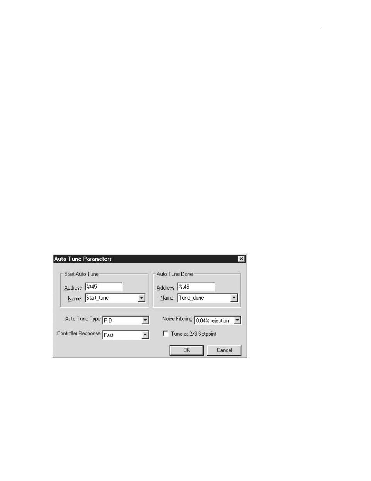
MAN0313-04 17 SEP 2002 PAGE 87
CH. 2
UP INPUT -- Enter a Register Type and Offset address or select a Named register that is the User-
controlled UP Input bit. This register is a Boolean (1 -bit) register, presumably %T.
DOWN INPUT -- Enter a Register Type and Offset address or select a Named register that is the User-
controlled DOWN Input bit. This register is a Bool ean (1-bit) register, presumably %T.
TUNE -- Click on the TUNE button to invoke the PID Element Tuning Dialog.
e. PID Autotune
The autotuning PID blocks add a number of new features to control the autotuning function. An edge
triggered boolean AUTOTUNE input starts the autotuning cycle. This input needs to be held high during
the autotuning cycle. If it is negated during the AUTOTUNE cycle, the controller stops autotuning and
reverts to the previous settings. At the conclusion of the AUTOTUNE cycle, the specified controller
coefficients are updated and the AUTOTUNE DONE output from the block is set to true. The PID block
now reverts to the previous state, either automatic or manual. At this point the AUTOTUNE input may be
removed which will cause the AUTOTUNE DONE output to be negated. The block will then be ready for
another autotune cycle. The new tuning coefficients are available in their respective registers.
Apart from the autotuning function, operation of the autotuning PID blocks is identical to that of the non autotuning PID blocks.
Auto tune PID allows the PID controller to perform an experiment on your process and use the results to
calculate PID coefficients that match your process and the desired PID operation.
When auto tune PID is enable this dialog allows the entry of auto tuning parameters:
Start Auto Tune - This is a Register Type and Offset that defines an input bit that controls when the
function should start the auto tune process.
Auto Tune Done - This is a Register Type and Offset that defines an output bit that is set by the
function when the auto tune is complete.
Auto Tune Type - This options allows the auto tune procedure to calculate terms for PID, PI or P
terms.
Page 88

PAGE 88 17 SEP 2002 MAN0313-04
CH. 2
Controller Response - This option defines the relative speed of the PID loop once it is tuned.
Noise Filtering - This option defines how far above and below the setpoint the process must go
when performing the auto tune experiment. Processes with more noise should be setup with a high
percentage.
Tune at 2/3 Setpoint - This allows the auto tuning experiment to change the output based on 2/3
the set point. Use this option when it is not desired for the process to travel above the setpoint during the
auto tuning experiment.
Using the Auto Tune Function
Prior to autotuning it is necessary to partially set up the PID block as before. Specifically, the Setpoint,
Sample Period, Upper and Lower Clamp, Error Term, and Output Polarity need to be set correctly. The
previous values of the proport ional, integral, and derivative coefficients do not affect the results of
autotuning.
The default settings for the autotune cycle produce Proportional, Integral, and Derivative coefficients
using the standard Ziegler -Nichols rules. This is suitable for many typical processes with delay and one
or two equal lags and with a fairly quiet process variable.
Non-default settings may be selected to improve the autotuning behavior in certain circumstances. These
selections only affect the generation of autotuning coefficients.
The controller type field defaults to PID but can be set to PI, Proportional/Integral, or just P, Proportional
control. PI control tends to be more stable with processes that do not have any delay, just lags. Full PID
control can give better response for processes with delay. The full PID tuning rules assume that the
process has a moderate delay and may not be suitable for other processes. These modes are produced
by the autotuning algorithm by setting the unused coefficients to zero. These may subsequently be
manually increased to enable the other modes.
The response field can be used to increase the controller damping to decrease overshoot and ringing.
For a typical Ziegler -Nichols process, the default FAST response produces some overshoot and a 4:1
decay ring down. MEDIUM produces a slight overshoot. SLOW produces no overshoot. With processes
that are outside the optimum range for Zeigler-Nichols rules, the VERY SLOW response may be
necessary for adequate response.
During autotuning the algorithm detects the process passing above and below the active setpoint.
Hysteresis is applied to the setpoint to the avoid false indications due to process noise. The default
hysteresis band is 0.04% of full scale. For noisy processes, this may need to be increased for proper
autotuning. the NOISE SUPPRESSION setting results in the following noise rejection values.
Higher noise rejection values also cause the autotuning algorithm to select somewhat slower, more stable
coefficients. For noisy processes, it is also recommended that PI rather than PID control be selected.
How Auto Tuning Works
The auto tuning function block performs and experiment on the process to be controlled and uses the
results to calculate the PID coefficients. While auto tuning the output is moved back and forth between
the upper and lower clamps. The time for the process to move from a percentage (based on noise
filtering) above and below the setpoint is recorded along with overshoot and undershoot readings. Once
this experiment is complete, the data collected is used to calculate the new PID coefficients.
Page 89
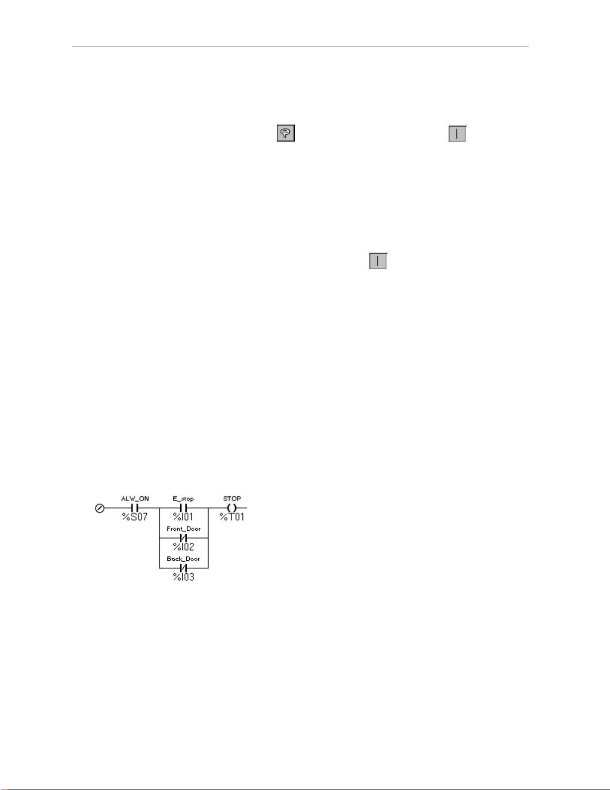
MAN0313-04 17 SEP 2002 PAGE 89
Warning: Removing a Vertical Branch can cause elements to be disconnected. Repair those flaws
CH. 2
2.19 Miscellaneous Elements
Miscellaneous Elements include Comments and the Vertical Branch.
2.19.1 Comments
Comments allow entering des criptive text into the program.
Comments can be downloaded to the controller. Comments do not affect the run time of the program, but
they can reduce the available memory in the controller if downloaded.
a. Add Vertical Branch
To insert a Vertical Continuation, click on the Vertical Branch tool. Note the change in the mouse
cursor.
Move the mouse cursor to the location where the Vertical Branch is designed, the single click the mouse.
b. Delete Vertical Branch
To delete a Vertical Branch, click on the Vertical Branch tool. Move the mouse cursor over the
continuation to be removed. When the cursor indicates a pencil eraser, single click the mouse.
before downloading the program.
EXAMPLE
The following code can be used as a safety interlock. Note the use of the Vertical Branch bars to provide
the logical OR handling of the three switches.
%I01 is a normally open manually activated switch. %I02 and %I03 represent safety interlock switches
that generate a logic HIGH when their associated door is CLOSED.
Vertical Branch
Thus, pressing E -stop OR opening Front_Door OR opening Back_Door generates the stop bit.
Page 90

PAGE 90 17 SEP 2002 MAN0313-04
CH. 2
NOTES
Page 91

MAN0313-04 17 SEP 2002 PAGE 91
CH. 3
CHAPTER 3: CSCAPE DATA TYPES
3.1 Overview
In Cscape , data can be stored or used in a variety of different formats. The format used depends on how
the information is to be interpreted. Typical interpretations are binary bit patterns, unsigned num bers,
signed numbers, floating point values, and strings.
3.2 Data Formats
Type Name Description
BOOL Boolean A single bit. It can contain only the values '0or '1'.
BYTE Byte A string of 8 consecutive bits. Byte values are used where the value
of the data is not as important as the bit patterns (shifts and
rotates).
WORD Word A string of 16 consecutive bits. Word values are used where the
value of the data is not as important as the bit patterns (s hifts and
rotates).
DWORD Double A string of 32 consecutive bits. Dword values are used where the
Word value of the data is not as important as the bit patterns (shifts and
rotates).
INT Integer A 16-bit signed value. Integers are used where the value of the data
is expected to be in the range of -32,768 to +32,767
SINT Short An 8-bit signed value. Short Integers are used where the value of
Integer the data is expected to be in the range of -128 to +127.
DINT Double A 32-bit signed value. Double Integers are used where the value of
Integer the data is expected to be in the range of -2,147,483,648 to
+2,147,483,647.
UINT Unsigned A 16-bit unsigned value. Unsigned Integers are used where the
Integer value of the data is expected to be in the range of 0 (zero) to
65,535.
USINT Unsigned An 8-bit unsigned value. Unsigned Short Integers are used where
Short the value of the data is expected to be in the range of 0 (zero) to
Integer 255
UDINT Unsigned A 32-bit unsigned value. Unsigned Double Integers are used where
Double the value of the data is expected to be in the range of 0 (zero) to
Integer 4,294,967,296.
REAL Floating A 32-bit value. Values are stored and operated on in IEEE single
Point precision (six digit) format. Values range from -3.40282E+38 to
+3.40282E+38.
STRING String A variable -length succession of characters. Each character is
Typically, any Data Type may use any Controller Register. For example a DINT value may use either
word (%R ) or Boolean (%I) registers. There is a restriction, however, if Boolean registers are used. In this
case, the value may be assigned only on a suitable boundary. For example, DWORD, DINT, and UDINT
values may be assigned to Boolean registers only on WORD (16 bit) boundaries -- 1, 17, 33, etc.
represented by one byte.
Page 92

PAGE 92 17 SEP 2002 MAN0313-04
CH. 3
Care must be taken when assigning non-Boolean data types to %I and %Q registers. For example, if a
WORD data type is assigned to %I registers, the I/O Scan of the controller will overwrite any change made
to the data by the Ladder Logic program. To prevent this, the programmer should insure that the data
assigned to %I point s is only read by the program (any data written will be over-written by the I/O Scan),
or that there is no physical I/O assigned to the %I locations used.
The bits in word registers may be used as Boolean values. In this case, Bit Offset Addressing is us ed to
specify the Register Type, Offset and Bit Offset for the required bit.
3.3 Storage Order
32-bit values (DWORD, DINT, UDINT) occupy 32 consecutive bits of data, or two (2 consecutive 16-bit
registers. For example, if a DINT is defined at Register %R43, the 32-bit value is contained in %R43 and
%R44.
For 32-bit values, data is stored Low Order Word first. For example, if a DINT is defined at Register
%R43 and contains the value "65540", (0000000000000001 0000000000000100) register %R43 will
contain "4" and %R44 will contain "1".
Byte values (such as STRINGS) are stored High Order Byte first. For example, to store the string "31" in
register %R43, store the HEX value 3133 (decimal 12595).
Page 93

MAN0313-04 17 SEP 2002 PAGE 93
CH. 4
CHAPTER 4: AVAILABLE CONTROLLER RESOURC ES
4.1 Overview
This chapter covers the Internal Resources of the OCS line of controllers.
4.2 Tables of Internal Resources
The following tables lists the Internal Resources of the GE Fanuc OCS line of controllers.
NOTE: This information is supplied for example and comparison purposes only and is subject to change
without notice. Refer to the User Manual included with the purchased controller model for complete up -
to-date information.
Text Based OCS Models
%I Registers 2048 2048 2048 2048 2048
%Q Registers 2048 2048 2048 2048 2048
%AI Registers 512 512 512 512 512
%AQ Registers 512 512 512 512 512
%IG Registers 64/0** 64/0** 64/0** 64/0** 64/0**
%QG Registers 64/0** 64/0** 64/0** 64/0** 64/0**
%AIG Registers 32/16** 32/16** 32/16** 32/16** 32/16**
%AQG Registers 32/16** 32/16** 32/16** 32/16** 32/16**
%T Registers 2048 2048 2048 2048 2048
%M Registers 2048 2048 2048 2048 2048
%R Registers 2048 2048 2048 9999*** 9999***
%K Registers 10 10 12 10 12
%D Registers 200 200 200 200 200
%S Registers 16 16 16 16 16
%SR Registers 64 64 64 64 64
Ladder Code memory 64K 64K 64K 128K 128K
Screen Memory 64K 64K 64K 128K 128K
Display 2x20 LCD
Keypad 16 17 32 17 32
Screens 200 200 200 200 200
Fields per Screen 16 16 16 16 16
Text Tables 200 200 200 200 200
Items per Table 20 20 20 20 20
Resource MiniOCS OCS100 OCS200 OCS110 OCS210
2x20 LCD
text
* RCS Models have no display or keypad, but the remote text term still allows viewing a virtual display and
keypad from Cscape.
** Devicenet models have 16 network words and no network bits. Device without networking capabilities have
no network registers.
*** Extended %R registers from 2049 to 9999 can currently only be used by move ladder instructions.
text
4x20 LCD
text
2x20 LCD
text
4x20 LCD
text
Page 94

PAGE 94 17 SEP 2002 MAN0313-04
CH. 4
Graphic OCS Models
Resource OCS250 0CS3xx
%I Registers 2048 2048
%Q Registers 2048 2048
%AI Registers 512 512
%AQ Registers 512 512
%IG Registers 64/0** 64/0**
%QG Registers 64/0** 64/0**
%AIG Registers 32/16** 32/16**
%AQG Registers 32/16** 32/16**
%T Registers 2048 2048
%M Registers 2048 2048
%R Registers 9999*** 9999***
%K Registers 10 5
%D Registers 300 300
%S Register s 16 16
%SR Registers 64 64
Ladder Code Memory 128K 256K
Graphic Objects Memory 256K 256K
String Memory 128K 128K
Text Table Memory 128K 128K
Bitmap Memory 256K 256K
Display 240x128 LCD
graphic
Colors 16 16
Keypad 36 6
Screens 300 300
Fields per Screen 50 50
Text Tables 200 200
Items per Table 20 20
320x240 LCD
STN or TFT
* RCS Models have no display or keypad, but the remote text term still
allows viewing a virtual display and keypad from Cscape.
** Devicenet models have 16 network words and no network bits. Device
without networking capabilities have no network registers.
*** Extended %R registers from 2049 to 9999 can currently only be used
by move ladder instructions.
Page 95

MAN0313-04 17 SEP 2002 PAGE 95
CH. 4
RCS Models
Resource MiniRCS RCS210
%I Registers 2048 2048
%Q Registers 2048 2048
%AI Registers 512 512
%AQ Registers 512 512
%IG Registers 64/0** 64/0**
%QG Registers 64/0** 64/0**
%AIG Registers 32/16** 32/16**
%AQG Registers 32/16** 32/16**
%T Registers 2048 2048
%M Registers 2048 2048
%R Registers 2048 2048
%K Registers 10 12
%D Registers 200 200
%S Registers 16 16
%SR Registers 64 64
Ladder Code memory 64K 64K
Display 2x20 Virtual* 4x20 Virtual*
Keypad 17 Virtual* 32 Virtual*
Screens 200 200
Fields per Screen 16 16
Text Tables 200 200
Items per Table 20 20
* RCS Models have no display or keypad, but the remote
text term still allows viewing a virtual display and keypad
from Cscape.
** Devicenet models have 16 network words and no
network bits. Device without networking capabilities have
no network registers.
*** Extended %R registers from 2049 to 9999 can
currently only be used by move ladder instructions.
4.3 Using More than 2048 %R Registers
Some controllers contain additional battery back RAM for extending %R registers beyond 2048.
Currently these additional registers beyond 2048 can only be used by move ladder instructions. This
allows ladder based data logging, recipes, or general storage to take advantage of the additional ret entive
memory.
The following is a list of instructions enabled for extended %R registers:
Move
Block Move
Block Fill
Indirect Move
Move Constant Data
Other features of Cscape that support the extended %R registers include I/O name management,
setpoints, watch window, debug, and element usage.
Note: These extended registers can not currently be directly displayed on the text or graphics display or
accessed by enhanced smart stack modules (Ethernet).
Page 96

PAGE 96 17 SEP 2002 MAN0313-04
CH. 4
NOTES
Page 97

MAN0313-04 17 SEP 2002 PAGE 97
CH. 5
CHAPTER 5: SYSTEM REGISTERS
5.1 General
System registers are special registers that display and/or control system operations in the controller.
5.2 System Registers
SR # Name Min Max
1 User Screen Number 0 200
2 Alarm Screen Number 0 200
3 System Screen Number 0 10
4 Self Test Result
5 Controller Mode (RUN) 0 2
6 Scan Rate Avg
7 Reserved
8 Reserved
9 Edit Buffer Low
10 Edit Buffer High
11 Ladder Size Low
12 Ladder Size High
13 User Text Size Low
14 User Text Size High
15 System Text Size Low
16 System Text Size High
17 I/O Config Size Low
18 I/O Config Size High
19 Net Config Size Low
20 Net Config Size High
21 Security Data Size Low
22 Security Data Size High
23 Ladder CRC
24 User Text CRC
25 System Text CRC
26 I/O Config CRC
27 Net Config CRC
28 Security Data CRC
29 Network ID Low 1 253
30 Reserved
31 Network Required 0 1
32 LCD Contrast 1 40
33 Key Toggle Mode 0 1
34 Serial Protocol
35 Serial Number Low
Serial Number High
Model Number
38 Engine Version
39 BIOS Version
40 FPGA Version
41 LCD Columns
42 LCD Rows
43 Keypad Type
44 RTC Seconds 0 59
Page 98

PAGE 98 17 SEP 2002 MAN0313-04
CH. 5
SR # Name Min Max
45 RTC Minutes 0 59
46 RTC Hours 0 23
47 RTC Day of Month 1 31
48 RTC Month 1 12
49 RTC Year 1996 2095
50 RTC Day of Week 1 7
51 Network Error Count
52-55 Reserved
56 Last Key
57 LCD Backlight
58 User LEDs
59-192 Reserved
SR01 User Screen Number
Ladder: Read/Write
Text: Rear/Write
Min: 0 Max: 200 (based on OCS200/ 100 as of printing)
This register displays/controls the current user scrollable screen. Setting this register to 0
displays no user screens.
SR02 Alarm Screen Number
Ladder: Read/Write
Text: Rear/Write
Min: 0 Max: 200 (based on OCS200/ 100 as of printing)
This register displays/controls the current alarm screen.
SR03 System Screen Number
Ladder: Read/Write
Text: Rear/Write
Min: 0 Max: 10 (based on OCS200/100 as of printing)
This register displays/controls the system screen. Setting this register to 0 displays no system
screen.
SR04 Self Test Result
Ladder: Read
Text: Read
This register displays the bit-mapped result of the self tests.
SR05 Controller Mode
Text: Read/Write
This register can display / control the RU N, DO I/O, or IDLE mode of the controller.
0 = IDLE 1 = DO I/O 2 = RUN
SR06 Scan Rate Avg
Ladder: Read
Text: Read
This register displays the average scan rate of the controller in tenths of milliseconds.
(123 = 12.3 mSec)
SR07 to SR0 8 RESERVED
Page 99

MAN0313-04 17 SEP 2002 PAGE 99
CH. 5
SR09 + SR10 Edit Buffer Low and High
Ladder: Read
Text: Read
This 32-bit register displays the intermediate value of a 1, 8, 16, or 32 -bit value being edited on
the text screen.
SR11 + SR12 Program Size Low and High
Ladder: Read
Text: Read
This 32-bit registers displays the number of bytes used by the currently loaded program.
SR13 + SR14 User Text Screen Size Low and High
Ladder: Read
Text: Read
This 32-bit registers displays the number of bytes used by the currently loaded user text screens
and text tables.
SR15 + SR16 System Text Screen Size Low and High
Ladder: Read
Text: Read
This 32-bit registers displays the number of bytes used by the currently loaded system text
screens.
SR17 + SR18 I/O Configuration Size Low and High
Ladder: Read
Text: Read
This 32-bit registers displays the number of bytes used by the currently loaded I/O configuration.
SR19 + SR20 Network Configuration Size Low and High
Ladder: Read
Text: Read
This 32-bit registers displays the number of bytes used by the currently loaded network
configuration.
SR21 + SR22 Security Data Size Low and High
Ladder: Read
Text: Read
This 32-bit registers displays the number of bytes used by the currently loaded security dat a.
SR23 Program CRC
Ladder: Read
Text: Read
This register displays the CRC value used for error detection for the currently loaded program.
SR24 User Text CRC
Ladder: Read Text: Read
This register displays the CRC value used for error detection for the currently loaded user text
screens and text tables.
SR25 System Text CRC
Ladder: Read
Text: Read
This register displays the CRC value used for error detection for the currently loaded system text
screens.
Page 100

PAGE 100 17 SEP 2002 MAN0313-04
CH. 5
SR26 I/O Confi guration CRC
Ladder: Read
Text: Read
This register displays the CRC value used for error detection for the currently loaded I/O
configuration.
SR27 Network Configuration CRC
Ladder: Read
Text: Read
This register displays the CRC value used for error detection for the currently loaded network
configuration.
SR28 Security Data CRC
Ladder: Read
Text: Read
This register displays the CRC value used for error detection for the currently loaded security
data.
SR29 Network ID
Ladder: Read
Text: Read/Write
Min: 1 Max: 253 (based on OCS200/100 in CsCAN mode as of printing)
This register displays or sets the controller's network ID.
SR30 RESERVED
SR31 Network Required
Ladder: Read
Text: Read
This register displays the status of the network required flag. If this value is a "1" the network is
required and any networking errors causes the controller to report an error. If this value is a 0
the network is not required and networking errors is ignored.
SR32 LCD Contrast
Ladder: Read
Text: Read/Write
Min: 1 Max: 40 (based on OCS200/100 as of printing)
This register allows the LCD contrast to be displayed or modified. This only applies to controllers
with LCD displays.
SR33 Key Toggle Mode
Ladder: Read/Write
Text: Read/Write
Min: 0 Max: 1 (based on OCS200/100 as of printing)
This register displays or sets the mode for the keyboard. When this register is a 0, the keypad is
in momentary mode. When this register is 1, it is in toggle mode. This only applies to controllers
with keypads.
 Loading...