

Page 1

Page 2

1INTRODUCTION ...................................
1 DESCRIPTION .....................................
2 ACCESSORIES .....................................
3INSTALLATION ....................................
3 SOFTWARE .......................................
3 BASE ADDRESS ....................................
4 WAIT STATE ......................................
4 AC INPUT FILTER ..................................
6PROGRAMMING ...................................
7 OUTPUT REGISTER .................................
8 INPUT REGISTER ...................................
9ELECTRONICS AND INTERFACING ..................
9 CONNECTOR DIAGRAM ............................
10 FORM C RELAY OUTPUTS .........................
10 FORM A RELAY OUTPUTS .........................
11 ISOLATED INPUTS ................................
12SPECIFICATIONS .................................
12 POWER CONSUMPTION ............................
12 RELAY SPECIFICATIONS ...........................
12 ISOLATED INPUTS ................................
13 ENVIRONMENTAL ................................
Page 3

INTRODUCTION
DESCRIPTION
The CIO-PDISO8 is an 8 channel isolated input, 8 channel relay output interface
board for the IBM PC and compatibles. The CIO-PDISO8 is designed for control and
sensing applications where a few points of high voltage need to be sensed or controlled.
WARNING!
High voltages will be present on the CIO-PDISO8 board when you
have connected high voltage inputs or outputs to the CIO-PDISO8
connector.
Use extreme caution! Never handle the CIO-PDISO8 when signals
are connected to the board through the connector.
DO NOT REMOVE THE PROTECTIVE PLATES FROM THE CIOPDISO8.
The outputs are 8 electromechanical relays. Five provide FORM C connection and
three provide normally open FORM A connection. The contacts are rated at 6A @
120V A.C. or 28V D.C., resistive load. The relays are controlled by writing to one 8
bit port. The state of the relay control register may be read back from the same port.
The inputs are 8 individual, optically isolated (500V) inputs that may be read back as
a single byte. The inputs are not polarity sensitive and may be driven by either A.C.
(50 - 1000 Hz) or D.C. in the range 5V - 24V R.M.S. Each input has a switchable
low-pass filter with a time constant of 5mS (200Hz).
Although requiring o nly two 8 bit ports, the CI O-PDISO8 occup ies 4 ports and will
appear at both locations. There is no need for this but that is how the original was
designed and the CIO-PDISO8 is a true clone.
Programming is accomplished by writes and reads to two 8 bit ports. Each bit indicates the state of an input or controls an output. Because the board is simple to program, requiring o nly tat the language you choose support direct register I/O, there is
no CALL routine or driver software supplied with the board. There are a few BASIC
examples.
1
Page 4

ACCESSORIES
The CIO-PDISO8 is a combination digital I/O board with signal conditioning
installed. Most accessory boards are intended to provide signal conditioning or easy
to access signal termination. In general, the CIO-PDISO8 with not require additional
signal conditioning.
We recommend that under no circumstance should a screw terminal board be used
with the CIO-PDISO8. The CIO-PDISO8 is intended to sense and control high voltages. If you use a screw terminal board you will expose yourself and others to those
high voltage signals.
We recommend that you construct a safe cable to carry you signals directly from your
equipment to the CIO-PDISO8 connector.
2
Page 5

INSTALLATION
SOFTWARE
INSTALL PROGRAM
On the disk labeled InstaCal there is an installation program. Please run SETUP .EXE
and accept the defaults. A new directory will be created on your hard disk and several
lines will be added to AUTOEXEC and CONFI G files. If you have purchased the
Universal Library for progra mming language InstaCAL will be installed as part of the
library installation. Please run SETUP.EXE form the Universal Library disk or CD.
Once all the software is installed, change to the CB directory and run InstaCal.
Choose the INSTALL menu and select your board by part number from the list. Supply the information required for base address and any other switch set or programmable features. Heed and act upon any warning messages displayed.
You may then run TEST and test the installation of the board. Follo w the instructions
for signal connection displayed on the screen.
You may also run CALIBRATE and check the calibr ation of the b oard, although that
is not necessary since the board was calibrated at the factory.
If you need it, there is some on-line help in the InstaCal program.
Owners of the Universal Library should read the manual and examine the example
programs prior to attempting any programming tasks.
BASE ADDRESS
The base address switch controls the I/O location where the CPU can access the registers of the CIO-PDISO8.
The factory default is 300H (768D).
If you have a board installed at address 300H, you will have to choose a new address
from those available on your computer. You may use the list of PC I/O address
assignments found elsewhere in thi s manual and ad d notes ab out the bo ards you have
installed in your computer.
3
Page 6

Choose a new base address from those
available and set the switch using the
guide to the right.
If 300H is available on your computer,
use it for the CIO-PDISO8. The software examples are written for base =
300H.
WAIT STATE
There is a wait state jumper on the CIO-PDISO8. The factory default is wait state disabled. You will probably never need the wait state because PC expansion slot busses
are limited to 8 or 10 MHz.
If you were to get intermittent operation from your PDISO8, you may try enabling the
wait state to see if that solves the problem.
AC INPUT FILTER
The inputs are 8 individual, optically isolated (500V) inputs that may be read back as
a single byte. The inputs are not polarity sensitive and may be driven by either A.C.
(50 - 1000 Hz) or D.C. in the range 5V - 24V R.M.S. Each input has a switchable
low-pass filter with a time constant of 5mS (200Hz).
The switch which controls the input filter is shown here.
The filter must be used for A.C. inputs and should be used for D.C. inputs
Unless you have reason to turn off a filter, we recommend it be left on.
The diagram here shows an A.C. signal without the input filter. This is how the signal
looks as it comes from the opto-isolator.
With the filter on, an A.C. voltage present on the input would produce a constant high
signal.
Your CIO-PDISO8 is set up and may be installed in the computer.
4
Page 7

WARNING!
High voltages will be present on the CIO-PDISO8 board when you
have connected high voltage inputs or outputs to the CIO-PDISO8
connector.
Use extreme caution! Never handle the CIO-PDISO8 when signals
are connected to the board through the connector.
DO NOT REMOVE THE PROTECTIVE PLATES FROM THE CIOPDISO8.
5
Page 8

PROGRAMMING
The CIO-PDISO8 is easy to program. Two eight bit registers located at the base
address (relay output) and base+1 (isolated inputs) are written to or read to control
relays, read back the state of relays or sense inputs.
BASE ADDRESS Relay Output Read/Write
BASE + 1 Isolated Inputs Read Only
BASE + 2 Not Used
BASE + 3 Not Used
Although the CIO-PDIS O8 d eco d es t o fo ur ad d re sses, two of those ar e no t use d . This
conforms to the design of the original PDISO-8, of which the CIO-PDISO8 is a true
clone.
The registers are written to and read from as a single 8 bit byte. Each bit controls and
output or represents the state of a device or input.
Both registers are read left to right. The leftmost bit being the most significant bit.
Following this format bit 7 of BASE+0 corresponds to relay 7 and bit 0 to relay 0.
To construct a control word, use the following table:
BIT No.
HEX Value
DECIMAL
To assemble a control byte:
If the relay status byte is read back, it is in the same format.
76543210
804020108421
1286432168421
6
ON=1DECIMALWEIGHTON=1HEXRELAY
WEIGHT
128112880180OP7
00640040OP6
3213220120OP5
00160010OP4
818818OP3
004004OP2
212212OP1
111111OP0
171AB
Page 9

The isolated inputs are read in this format as well. To disassemble the byte and determine the state of the isolated inputs or the relay read back register, perform the following operation in software:
HEXINPUT/RELAY
Perform an AND operation for each bit to see if it is on.. In this example the variable
INPBYTE% is the isolated input byte read from BASE+1. This example is in Microsoft Basic.
INPBYTE% = INP(BADR+1)
INP7% = INPBYTE% AND &H80
IF INP7% = 1 THEN ISOINP$ = "ON" ELSE ISOINP$ = "OFF"
The code above shows how to set the variable INP7% to either 1 or 0. It may then be
used in your program. The variable ISOINP$ may be used as part of your on-screen
display. Other programming example follow.
DECIMAL
12880IP7/OP7
6440IP6/OP6
3220IP5/OP5
1610IP4/OP4
88IP3/OP3
44IP2/OP2
22IP1/OP1
11IP0/OP0
OUTPUT REGISTER
The output register is located at the CIO-PDISO8 base address.
WRITE = CONTROL: Write a byte to the register to control the relays. A one in the
relay bit position turns the relay on.
READ = STATUS: Read the status of the relay control register. A one in the relay
bit position indicates the relay is on.
ON & OFF for FORM C RELAYS:
On means that FORM C relay common is in contact with the Normally Open contact.
Off means that FORM C relay common is in contact with the normally closed contact.
ON & OFF FOR FORM A RELAYS:
On means that FORM A relay common is in contact with the normally open contact.
Off means that FORM A common is not in contact with anything.
7
Page 10

RELAY OP7 OP6 OP5 OP4 OP3 OP2 OP1 OP0
BIT No. 76543210
HEX Value 804020108421
DECIMAL 1286432168421
INPUT REGISTER
The isolated input register is located at the CIO-PDISO8 base address + 1.
WRITE = NO FUNCTION
READ = STATUS: Read the status of the isolated inputs. A one in the input bit position indicates that a voltage is present at the input.
INPUT #
BIT No. 76543210
HEX Value 804020108421
DECIMAL 1286432168421
IP7 IP6 IP5 IP4 IP3 IP2 IP1 IP0
8
Page 11
ELECTRONICS AND INTERFACING
This short, simple introduction to the electronics most often needed by digital I/O
board users covers a few key concepts. They are:
• Connector diagram.
• FORM C relay outputs.
• FORM A relay outputs.
• Isolated inputs.
• Adding a resistor to expand the range of the isolated inputs.
• Voltage dividers.
• Low pass filters for digital inputs.
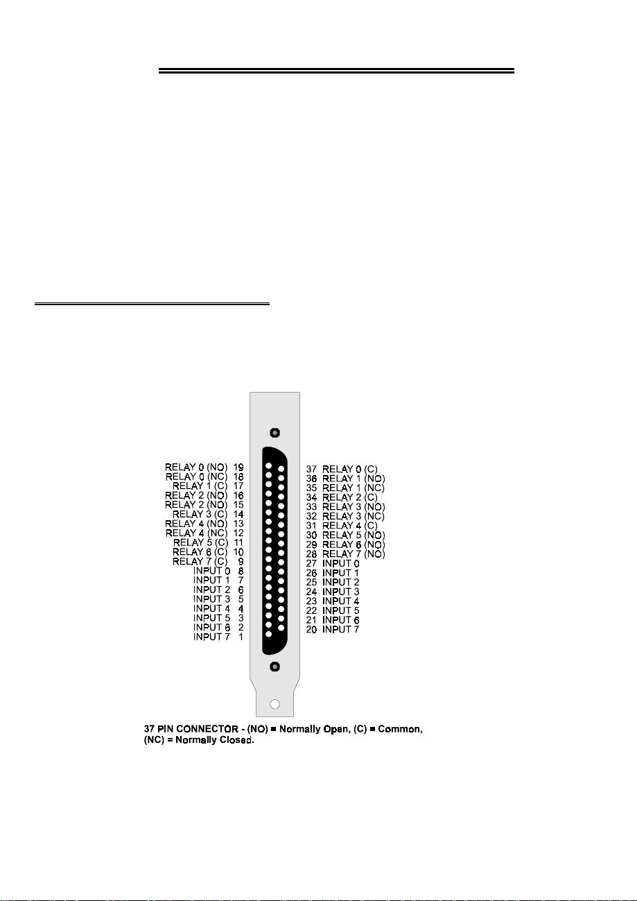
CONNECTOR DIAGRAM
The CIO-PDISO8 use a single 37 pin connector for signal interfacing. The pin-outs
of the connector are shown below.
9
Page 12
WARNING!
High voltages will be present on the CIO-PDISO8 board when you
have connected high voltage inputs or outputs to the CIO-PDISO8
connector. Use extreme caution! Never handle the CIO-PDISO8
when signals are connected to the board through the connector.
DO NOT REMOVE THE PROTECTIVE PLATES FROM THE CIOPDISO8.
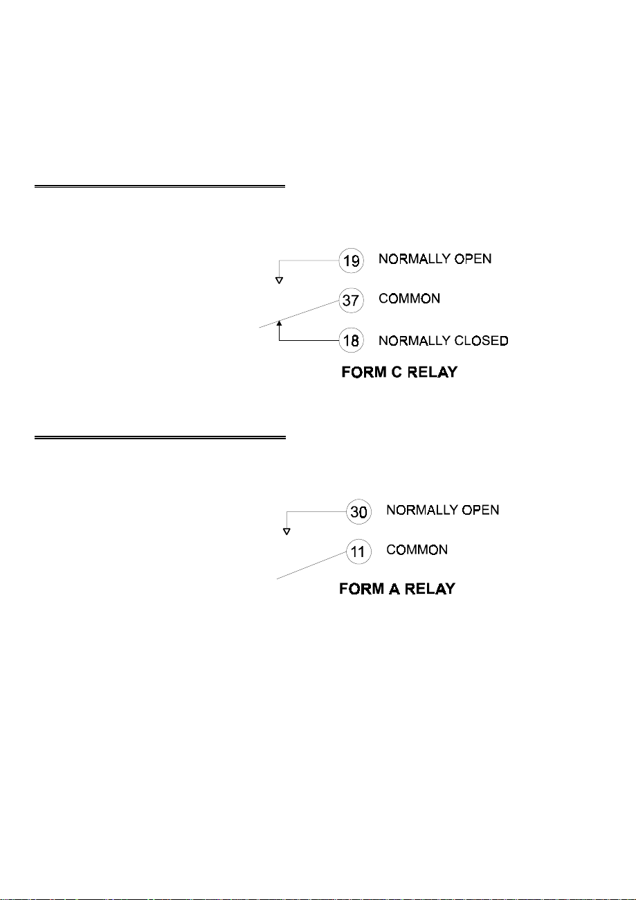
FORM C RELAY OUTPUTS
Shown here is the schematic for a
form C relay, like those connected at
OP0 through OP4.
The form C relay has a COMMON,
normally open (NO) and normally
closed (NC) contact.
When a 0 is written to the output, the
common and NC are in contact.
When a 1 is written to the output the common and NO are in contact.
FORM A RELAY OUTPUTS
Shown here is the schematic for a form
A relay, like those connected at OP5
through OP7.
The form A relay has a COMMON and
a normally open (NO) contact.
When a 0 is written to the output, the
common and NO are NOT in contact.
When a 1 is written to the output the common and NO are in contact.
The form A and form C relays on the CIO-PDISO8 are the same part. Only the connections to the relay poles differ.
The specifications for both types of relays are:
Contact rating 6A @ 120V A.C or 28V D.C. resistive
Contact type Gold overlay silver
10
Page 13
Contact resistance 100 miliohms max.
Operate time 20 miliseconds
Release time 10 miliseconds max.
Life expectancy 10 million mechanical operations min.
100,000 electrical at full load min.
ISOLATED INPUTS
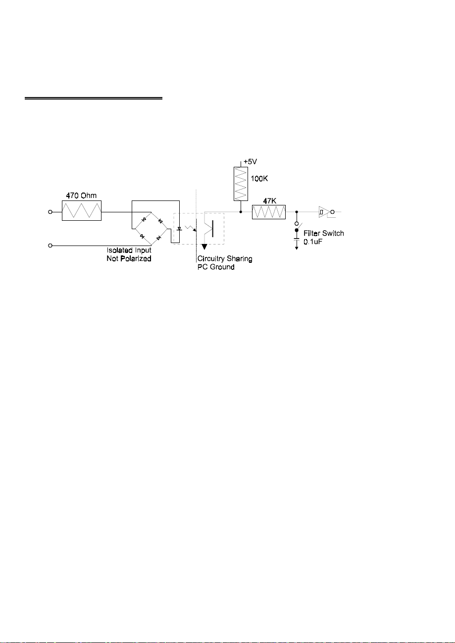
There are 8 isolated input channels. The schematic of a single channel is shown here.
The signals are r o ute d thr o ugh a b ri d ge r ec tifie r so tha t the inp uts ar e no t p o lar it y sensitive.
The specifications for an input are:
Range 5-24V D.C.
5-24V A.C. (50-1000Hz)
NOT TTL compatible.
Isolation 500V
Resistance 470 ohm min
Response 20 uSeconds w/o filter
5 miliseconds w/ filter
11
Page 14

SPECIFICATIONS
POWER CONSUMPTION
+5V supply 0.3A typical with all relays off.
1.0A typical with all relays on.
±12V Supply Not used
RELAY SPECIFICATIONS
Number 8
Contact arrangement 5 form C, OP0 - OP4
3 form A, OP5 - OP7
Contact rating 6A @ 120V A.C or 28V D.C. resistive
Contact type Gold overlay silver
Contact resistance 100 miliohms max.
Operate time 20 miliseconds
Release time 10 miliseconds max.
Life expectancy 10 million mechanical operations min.
Vibration 10 to 55 Hz (Dual amplitude 1.5mm)
Shock 10G (11 miliseconds)
Dielectric isolation 500V (1 minute)
Life Expectancy 1 Million Operations Electrical
100,000 Operations @ Full Load
ISOLATED INPUTS
Number 8
Range
Isolation 500V
Resistance 470 ohm min
Response 20 uSeconds w/o filter
5-24V D.C. or A.C. (50-1000Hz)
NOT TTL compatible.
5 miliseconds w/ filter
12
Page 15

ENVIRONMENTAL
Operating temperature 0 to 50 deg. C
Storage temperature -20 to 70 deg. C
Humidity 0 to 90% non-condensing
Weight 8 oz.
Size 3 7/8" (99mm) tall excluding gold fingers
6 1/2" (164mm) long
13
 Loading...