

Page 1

User's Guide
http://www.omega.com
e-mail: [email protected]
CIO-DIO48
CIO-DIO48H
CIO-DIO96
CIO-DIO192
Page 2
Cable from DIO board
g
g
g
g
g
s into connector
plu
IN
labeled
Cable from DIO board
s into connector
plu
IN
labeled
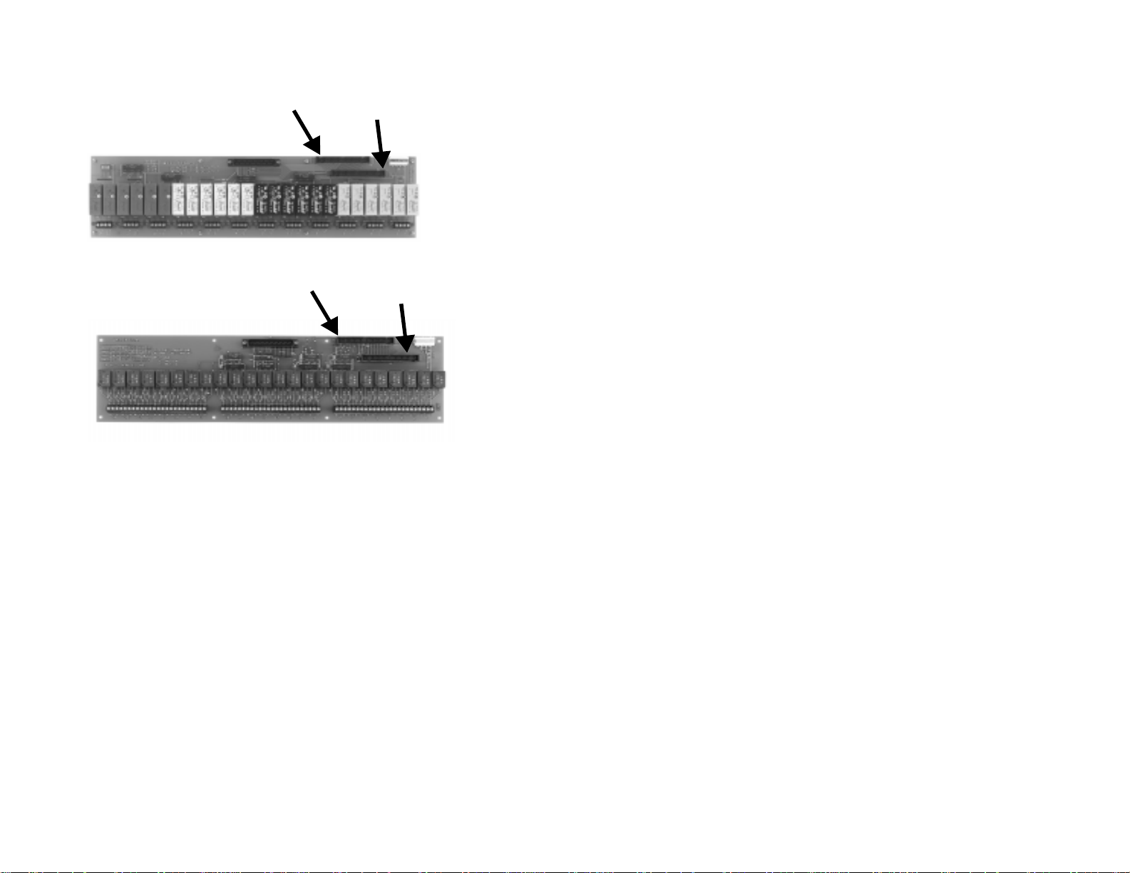
CIO-ERB-24 and SSR-RACK24 provide connectors
allowin
a single CIO-DIO-48 style board to control or
monitor two 24-bit relay/SSR boards.
Cable to second E R B or
SSR board plu
connector labeled
Cable to second E R B or
SSR board plu
connector labeled
s into
OUT
s into
OUT
TM
.....................................
......................................
......................................
..................................
...............
.......................
........................
..........................
................................
......................
..........................
...............................
........................................
......................
.........................
..........................
.................................
..................
....................
1INTRODUCTION ...................................
2QUICK START .....................................
2 INSTALL THE INSTACALTM SOFTWARE
2 RUN INSTACAL
4OPERATION .......................................
4 INSTALLATION
4 BASE ADDRESS
6 WAIT STATE JUMPER
6 INSTALLING THE CIO-DIO IN THE COMPUTER
7 CABLING TO THE DIO CONNECTOR
7 SIGNAL CONNECTION - CIO-DIO48
8 UNCONNECTED INPUTS FLOAT
8 CONNECTOR DIAGRAM
9ARCHITECTURE ...................................
9 82C55 CONTROL & DATA REGISTERS
11 82C55 DIGITAL I/O REGISTERS
14SPECIFICATIONS .................................
14 POWER CONSUMPTION
15 DIGITAL I/O
16ELECTRONICS AND INTERFACING .................
16 PULL UP & PULL DOWN RESISTORS
18 UNCONNECTED INPUTS FLOAT
18 TTL TO SOLID STATE RELAYS
19 VOLTAGE DIVIDERS
21 LOW PASS FILTERS DE-BOUNCE INPUTS
22CIO-ERB24 & SSR-RACK24 CONNECTIONS ..........
Page 3
INTRODUCTION
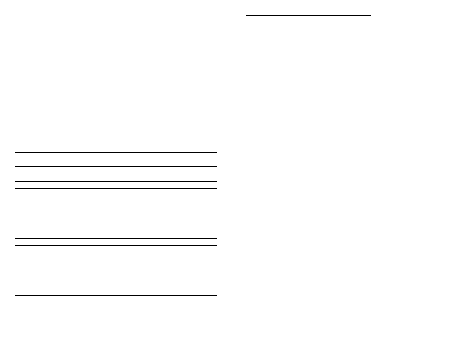
CIO-ERB24 & SSR-RACK24 CONNECTIONS
This manual provides complete information on CIO-DIO48, CIO-DIO48H, CIODIO96 and CIO-DIO192 digital I/O boards and accessories. The manual is organized
into separate sections for those aspects of a product which are unique. Some issues,
such as BASIC programming and electronic interfacing are applicable to all of the
digital boards.
The CIO-DIO48 has two 82C55 parallel interface chips and a 50 pin connector. Each
82C55 controls 24 CMOS/TTLcompatible digital I/O pins. Within each 82C55, the
digital I/O lines may be programmed as groups of 8,8 & 8 or 8,8 & 4,4. Each group
may be input or output.
The CIO-DIO96 provides two CIO-DIO48 circuits on a single board while he CIODIO192 provides 4 CIO-DIO48 circuits on a single board. The CIO-DIO48H is a
high drive, 48 line digital I/O board built up of logic chips. The control registers
which set the direction of the I/O ports are identical to 82C55 mode 0 control registers
(like those on the CIO-DIO48 in mode 0). The I/O lines are high drive, capable of
sourcing 15mA and sinking 64mA.
Each of the boards have the same connector pin-out and respond to the same software
instructions. This manual includes information on programming the 82C55 in mode 0.
Those wishing to use the 82C55 in modes 1 or 2 must procure a data book from Intel
Corporation Literature Department.
The boards may either be programmed with direct I/O register reads and writes, or all
mode 0 functionality is provided by the optional UniversalLibrary driver software.
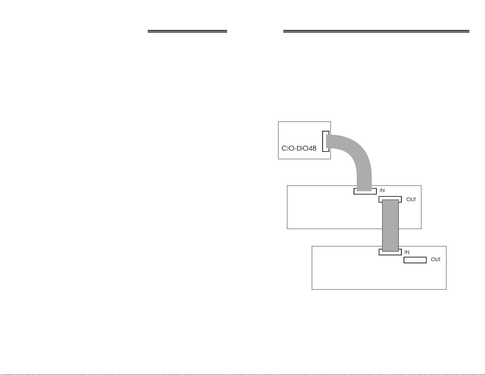
CIO-DIO48 family boards each provide digital I/O in groups of 48 bits. However, the
most popular relay and SSR boards provide only 24-bits of I/O. The CIO-ERB24 and
SSR-RACK24 each implement a connector scheme where all 48 bits of the CIO-DIO
board may be used to monitor and control relays and/or SSRs. This configuration is
shown in the block diagram below. The 24-bits of digital I/O on CIO-DIO connector
pins 1-50 (base address +0 through +3) control the first relay board. The 24-bits of
CIO-DIO on pins 51-100 will control the second relay/SSR board on the daisy chain.
&,2',2
,1
CIO-ERB24
287
or
SSR-RACK24
The goal of this manual is to assist you in your application of a CIO board to your
sensing or control problem. We are interested in your corrections and suggestio ns and
will implement them.
1
CIO-ERB24
or
SSR-RACK24
22
,1
287
Page 4
LOW PASS FILTERS DE-BOUNCE INPUTS
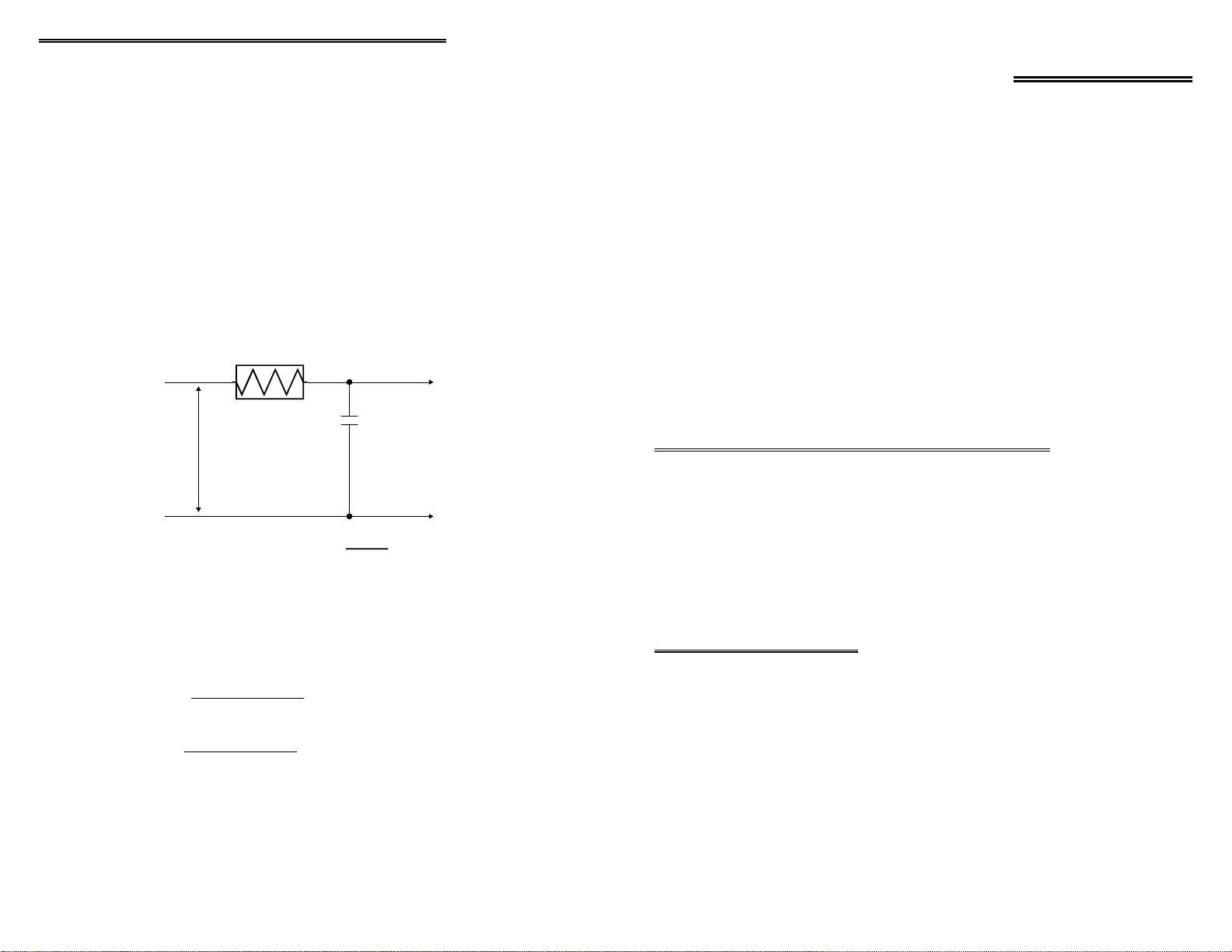
A low pass filter is placed on the signal wires between a signal and an A/D board. It
stops frequencies greater than the cut off frequency from entering the A/D board's
analog or digital inputs.
The key term in a low pass filter circuit is cut off frequency. The cut of frequency is
that frequency above which no variation of voltage with respect to time may enter the
circuit. For example, if a low pass filter had a cut off frequency of 30 Hz, the kind of
interference associated with line voltage (60Hz) would be filtered out but a signal of
25Hz would be allowed to pass.
Also, in a digital circuit, a low pass filter might be used to de-bounce an input from a
momentary contact button pushed by a person.
Signal
Hig h
Signal
Volts
Signal
Low
LO W PAS S F ILTE R - F = 1
2*Pi*R*C
R
C
To I/O bo a rd
c
A low pass filter may be constructed from one resistor (R) and one capacitor (C). The
cut off frequency is determined according to the formula:
Fc = 1
2 * Pi * R * C
R = 1
2 * Pi * C * F
Where Pi = 3.14
c
QUICK START
The installation and operation of all three of the CIO-DIO series boards is very
similar. Throughout this manual we use CIO-DIO as a generic designation for the
CIO-DIO48, CIO-DIO48H, CIO-DIO96 and CIO-DIO192. When required due to the
differences in the boards, the specific board name is used.
The CIO-DIO boards are easy to use. This quick start procedure will help you quickly
and easily setup, install and test your board. We assume you already know how to
open the PC and install expansion boards. If you are unfamiliar or uncomfortable with
board installation, please refer to your computer’s documentation.
We recommend you perform the software installation described in
sections 1.1 and 1.2 below prior to installing the board in your
computer.
The
InstaC
properly set the switches and jumpers on the board prior to physically installing the board in your computer.
INSTALL THE INSTACALTM SOFTWARE
Windows 95, 9 8 or NT users install the p rogram by running the setup.exe pr ogram
supplied with your DIO software. (DOS and Windows 3.x users need to run
INTSTALL.EXE) It will create all required folders/directories and unpack the various
pieces of compressed software. Simply run install and follow the on-screen instructions. Remember where the installed files are placed, as you will need to access them
in the next step (the default location is on your main hard drive in a directory or folder
named C:\CB\).
INSTA
RUN
To run
Insta
using your file management system and do ub le cli ck your mouse on i t. In DO S simply
instacal
type
Once running,
1. Select
mouse on it).
TM
Cal
and press the
Insta
CAL
in the various forms of Windows, find the file named InstaCal.exe
TM
provides four sub-menus (plus exit).
Cal
Install
(either highlight it and hit enter of double click your
TM
Enter
TM
operations below will show you how to
al
key.
21
2
Page 5

2. Select Board #0 (select another number if Board #0 is already installed)
3. Select Board Type
4. Move through the selections and highlight the particular board you
are installing (e.g. CIO-DIO48H or CIO-DIO192).
Either double click on the board or hit enter.
5. The board’s default settings are then displayed. The board’s defaults are:
Attenuation = R1 + R2
R2
2 = 10K + 10K
10K
The variable Attenuation is the proportional difference between the signal voltage max and the full
scale of the analog input.
For example, if the signal varies between 0 and 20
volts and you wish to measure that with an analog
input with a full scale range of 0 to 10 volts, the
Attenuation is 2:1 or just 2.
BASE ADDRESS: 300H (768 Decimal) Same as data sheet.
WAIT STATE: OFF.
6. You are now ready to install the board in your computer. Open your PC (after
turning off the power) and install the board. After the board is installed and the
computer is closed up, turn the power back on.
7. Run InstaCal
TM
again, and at the main menu select Test.
a. Select the board you just installed
b. Select Internal Test
c. The internal control registers of the board will then be tested. If this test
is successful, your board is installed correctly. If not, you likely have
a base address conflict, or have the base address switch set incorrectly.
Please refer to the next chapter for more information regarding selecting
and setting the base address.
d. If the Internal Test is completed successfully, you may want to check
that the I/O pins are working correctly. To check this select
External Test and follow the instruction provided. This will
require you to use the shorting wires supplied with the board to
short inputs to outputs for I/O testing.
R1 = (A - 1) * R2
For a given attenua tion, pick a handy resistor and
call it R2, then use this formula to calculate R1.
Digital inputs also make use of voltage dividers, for example, if you wish to measure a
digital signal that is at 0 volts when off and 24 volts when on, you cannot connect that
directly to the CIO-DIO digital inputs. The voltage must be dropped to 5 volts max
when on. The Attenuation is 24:5 or 4.8. Use the equation above to find an appropriate R1 if R2 is 1K. Remember that a TTL input is 'on' when the input voltage is
greater than 2.5 volts.
IMPORTANT NOTE: The resistors, R1 and R2, are going to dis-
sipate all the power in the divider circu it according to th e equation
Current = Voltage / Resistance. The higher the value of the resistance (R1 + R2) the less power dissipated by the divider circuit.
Here is a simple rule:
For Attenuation of 5:1 or less, no resistor should be less than 10K.
For Attenuation of greater than 5:1, no resistor should be less than
1K.
The CIO-TERMINAL has the circuitry on board to create custom voltage dividers.
The CIO-TERMINAL is a 16" by 4" screw terminal board with two 37 pin D type
connectors and 56 screw terminals (12 - 22 AWG). Designed for table top, wall or
rack mounting, the board provides prototype, divider circuit, filter circuit and pull-up
resistor positions which you may complete with the proper value components for your
application.
3
20
Page 6
Voltage = Current * Resistance (commonly V=IR)
g
g
g
and Kirkoff's voltage law which states,
The sum of the voltage drops around a circuit will be equal to the
voltage drop for the entire circuit.
OPERATION
Implied in the above is that any variation in the voltage drop for the circuit as a whole
will have a proportional variation in all the voltage drops in the circuit.
A voltage divider takes advantage of the fact that the voltage across one of the resistors in a circuit is proportional to the voltage across the total resistance in the circuit.
Signal
Hi
h
Si
nal
Vin
Volts
Si
nal
L ow
SIMPLE VOLTAGE DIVIDER - Vin = R1+R2
R1
R2
V1
V2
Vout
Vout R2
To the I/O Board
The trick to using a voltage divider is to choose two resistors with the proper proportions relative to the full scale of the digital input and the maximum signal voltage.
The phenomena of dropping the voltage proportionally is often called attenuation.
The formula for attenuation is:
INSTALLATION
The CIO-DIO48 has two 82C55 parallel interface chips and a 50 pin connector. Each
82C55 controls 24 CMOS TTL digital I/O pins. Within each 82C55, the digital I/O
lines may be programmed as groups of 8,8 & 8 or 8,8 & 4,4). Each group may be
input or output.
The CIO-DIO96 is exactly two CIO-DIO48 circuits on a single board.
The CIO-DIO192 is exactly 4 CIO-DIO48 circuits on a single board.
All three boards share in common a base address switch, wait state jumper and 50 pin
connector(s)
BASE ADDRESS
InstaCAL will help you select and set the board’s base address. Insta CAL allows you
to choose a desired base address and adjusts the base address if necessary to place it
on an 8 bit boundary, CIO-DIO48, 16 bit boundary, CIO-DIO96 or 32 bit boundary,
CIO-DIO192
The CIO-DIO employs the PC bus
for power, communications and
data transfer. As such it draws
power from the PC, monitors the
address lines and control signals
and responds to it's I/O address,
and it receives and places data on
the 8 data lines.
The BASE address is the most
important user selectable bus
related feature of the CIO-DIO. The base address is the location that software writes
to and reads from when communicating with the CIO-DIO.
19
4
Page 7
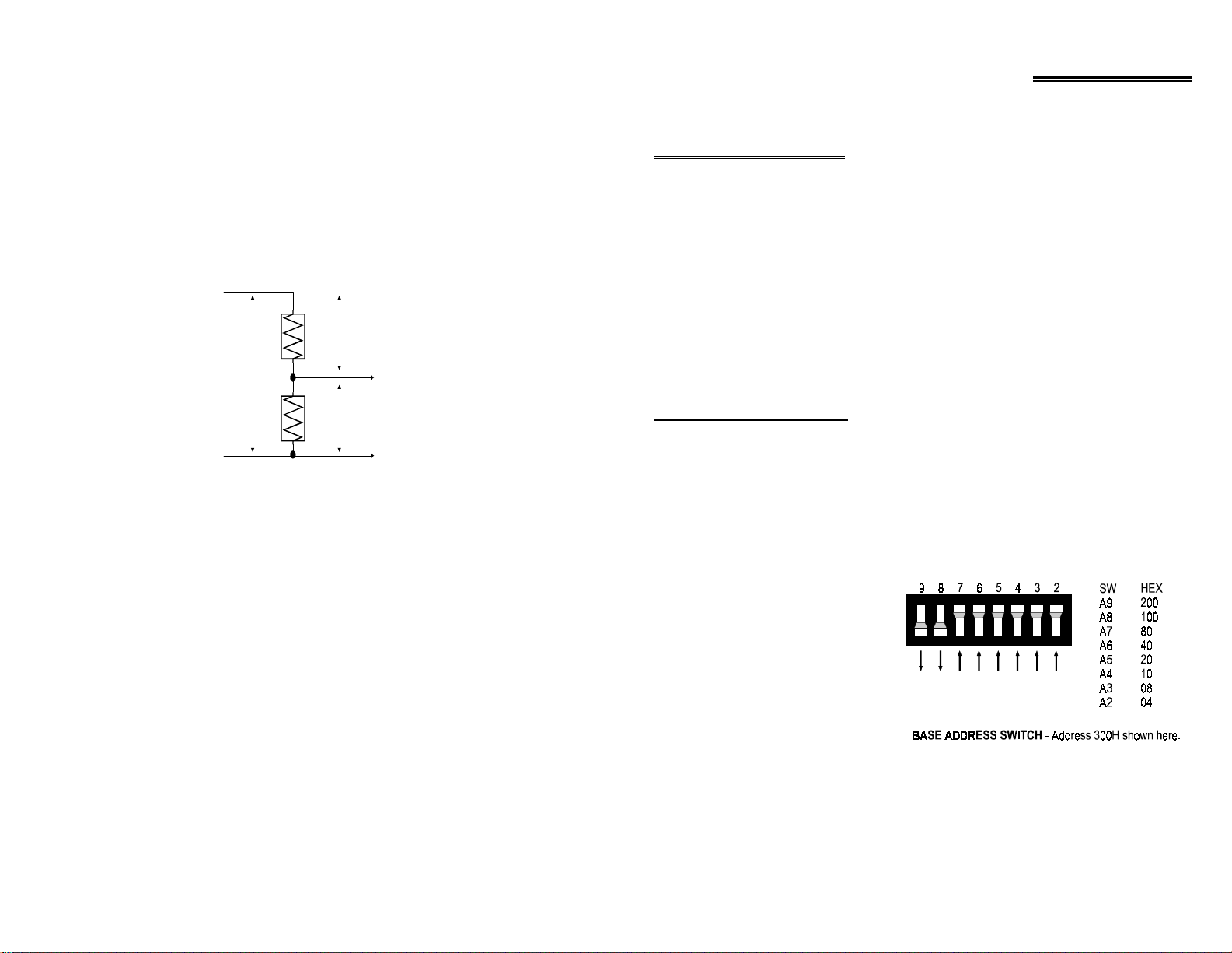
The base addr ess switch is the means for setting the base addre ss. Each switch position corresponds to one of the PC bus address lines. By placing the switch down, the
CIO-DIO address decode logic is instructed to respond to that address bit.
A complete address is constructed by calculating the HEX or decimal number which
corresponds to all the address bits the CIO-DIO has been instructed to respond to.
For example, shown to the right are address 9 and 8 DOWN, all others UP.
Address 9 = 200H (512D) and address 8 = 100H (256D), when added together they
equal 300H (768D).
UNCONNECTED INPUTS FLOAT
Keep in mind that unconnected inputs float. If you are using a DIO board for input,
and have unconnected inputs, ignore the data from those lines.
In other words, if you connect bit A0 and not bit A1, do not be surprised if A1 stays
low, stays high or tracks A0... It is unconnected and so is not specified. The 82C55 is
not malfunctioning. In the absence of a pull-up/down resistor, any input to a CIODIO which is unconnected is unspecified.
NOTE
DO NOT PAY ATTENTION TO THE NUMBERS PRINTED ON
THE SWITCH. LOOK AT THE NUMBERS PRINTED IN WHITE
ON THE BOARD!
Certain addresses are used by the PC, others are free and may be used by the CIODIO and other expansion boards. We recommend BASE = 300H (768D) be tried
first.
FUNCTIONHEX
EGA2C0-2CF8237 DMA #1000-00F
EGA2D0-2DF8259 PIC #1020-021
GPIB (AT)2E0-2E78253 TIMER040-043
SERIAL PORT2E8-2EF82C55 PPI (XT)060-063
SERIAL PORT2F8-2FF8742 CONTROLLER (AT)060-064
PROTOTYPE CARD300-30FCMOS RAM & NMI
PROTOTYPE CARD310-31FDMA PAGE RESISTERS080-08F
HARD DISK (XT)320-32F8259 PIC #2 (AT)0A0-0A1
PARALLEL PRINTER378-37FNMI MASK0A0-0AF
SDLC380-38F8237 #2 (AT)0C0-0DF
SDLC3A0-3AF80287 NUMERIC CO-P
MDA3B0-3BBHARD DISK (AT)1F0-1FF
PARALLEL PRINTER3BC-3BFGAME CONTROL200-20F
EGA3C0-3CFEXPANSION UNIT (XT)210-21F
CGA3D0-3DFBUS MOUSE238-23B
SERIAL PORT3E8-3EFALT BUS MOUSE23C-23F
FLOPPY DISK3F0-3F7PARALLEL PRINTER270-27F
SERIAL PORT3F8-3FFEGA2B0-2BF
RANGE
070-071
0FF-0FF
FUNCTIONHEX
RANGE
MASK (AT)
(AT)
You do not have to tie input lines, and unconnected lines will not affect the performance of connected lines. Just make sure that you mask out any unconnected bits in
software.
TTL TO SOLID STATE RELAYS
Many applications require digital outputs to switch AC and DC voltage motors on and
off and to monit or AC and DC vo ltages. T hese AC and high D C voltages c annot be
controlled or read directly by the TTL digital lines of a CIO-DIO.
Solid State Relays, allow control and monitori ng of AC and high DC volta ges and
provide 750V isolation. Solid State Relays (SSRs) are the recommended method of
interfacing to AC and high DC signals.
The most convenient way to use solid state relays and a CIO-DIO board is to purchase
a Solid State Relay Rack. A SSR Rack is a circuit board with output buffer chips
which are powerful enough to switch the SSR and sockets to plug SSRs into.
SSR Racks are available from most manufacturers of SSRs.
If you only want to drive one or two SSRs, all you need is a 74LS244 output buffer
chip between the 82C55 output and the SSR. Of course the SSR will need a 5 volt
power source as well.
VOLTAGE DIVIDERS
If you wish to measure a signal which varies over a range greater than the input range
of a digital input, a voltage divider can drop the voltage of the input signal to the level
the digital input can measure.
A voltage divider takes advantage of Ohm's law, which states,
5
18
Page 8
If the inputs of the device you are controlling are left to float, they may float up or
down. Which way they float is dependent on the characteristics of the circuit and the
electrical environment; and unpredictable! This is why it often appears that the 82C55
has gone 'high' after power up. T he result is that your controlled device gets turned
on!
That is why you need pull up/down resistors.
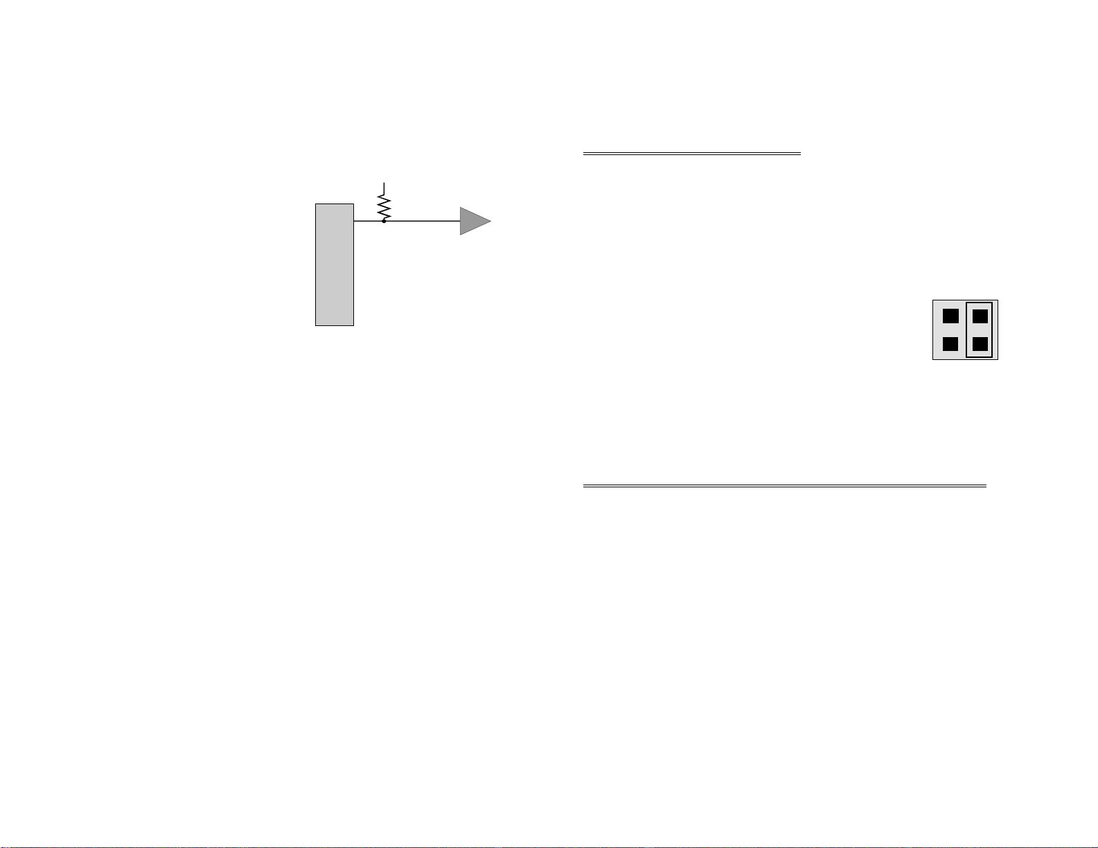
Shown here is one 82C55 digital output
with a pull-up resistor attached.
If the 82C55 is reset and enters high imped-
82C55
A0
+5V
2.2K
Controlled
Device
ance input, the line is pulled high. At that
point, both the 82C55 AND the device
being controlled will sense a high signal.
If the 82C55 is in output mode, the 82C55
has more than enough power to over ride
82 C5 5 Dig ita l O utp ut with
pull-up resistor attached
the pull-up resi stor's high signal and drive
the line to 0 volts. If the 82C55 asser ts a high signal, the pull up resistor guaranties
that the line goes to +5V.
The CIO-DIO BASE switch may be set for address in the range of 000-3F0 so it
should not be hard to find a free address area for you CIO-DIO. Once again, if you
are not using IBM prototyping cards or some other board which occupies these
addresses, then 300-31F HEX are free to use.
Addresses not specifically listed, such as 390-39F, are free.
WAIT STATE JUMPER
Some CIO-DIO boards have a wait state jumper which can enable an on-board wait
state generator. A wait state is an extra delay injected into the processor's clock via
the bus. This delay slows down the processor when the processor addresses the CIODIO board so that signals from slow devices (chips) will be valid.
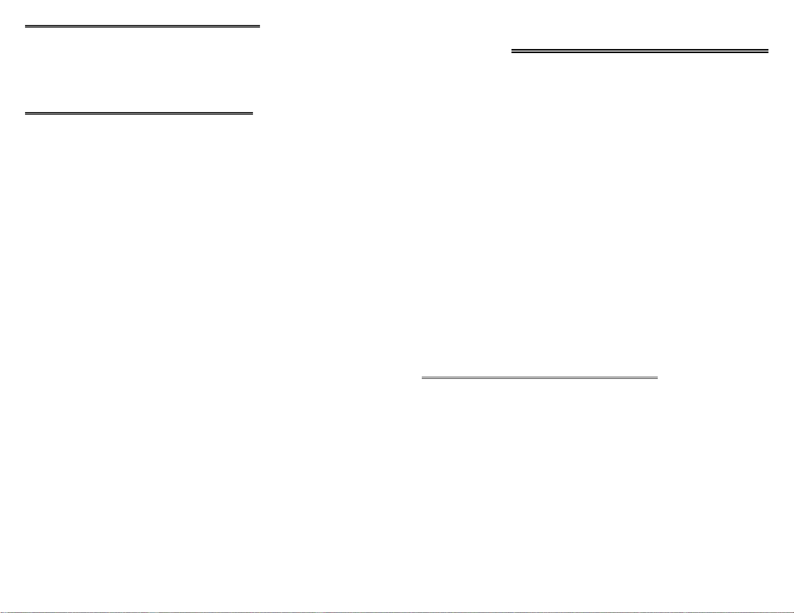
The wait state generator on the CIO-DIO is only
active when the CIO-DIO is being accessed. Your
PC will not be slowed down in general by using
the wait state.
Because all PC expansion board buses are slowed
to either 8MHz or 10MHz, the wait state will generally not be required.
WAIT STATE JUMPER BLOCK
ON OFF
Of course, a pull-down resistor accomplishes the same task except that the line is
pulled low when the 82C5 5 is r ese t. T he 8 2 C5 5 ha s more than e nough p o wer to dr ive
the line high.
The CIO-DIO boards are equipped with positions for pull-up/down resistors Single
Inline Packages (SIPs). The positions are marked A, B and C and are located beside
the 82C55.
A 2.2K ohm, 8 resistor SIP is made of 8, 2.2K resistors all connected on one side to a
common point and on the other, to a pin protruding from the SIP. The common line to
which all resistor are connected also protrudes from the SIP. The common line is
marked with a dot and is at one end of the SIP.
The SIP may be installed as pull-up or pull-down. At each location, A, B & C there
are 10 holes in a line. One end of the line is +5V, the other end is GND. They are so
marked. The 8 holes in the middle are connected to the 8 lines of the port, A, B, or C.
Install and solder the SIP in place.
A resistor value of 2.2K is recommended. Use other values only if you have calculated
the necessity of doing so.
17
If you experience sporadic errors from the 82C55 digital I/O chip (reset, port direction
swaps) you might try enabling the wait state generator.
INSTALLING THE CIO-DIO IN THE COMPUTER
Turn the power off.
Remove the cover of your computer. Please be careful not to dislodge any of the
cables installed on the boards in your computer as you slide the cover off.
Locate an empty expansion slot in your computer.
Push the board firmly down into the expansion bus connector. If it is not seated fully
it may fail to work and could short circuit the PC bus power onto a PC bus signal.
This could damage the motherboard in your PC as well as the CIO-DIO.
6
Page 9
CABLING TO THE DIO CONNECTOR
The CIO-DIO48 connector is accessible through the PC/AT exp ansion bracket. The
connector is a standard 50 pin male header connector. A mating female connector
may be purchased at Radio Shack or other electronic supply outlets.
ELECTRONICS AND INTERFACING
This short, simple introduction to the electronics most often needed by digital I/O
board users covers a few key concepts. They are:
SIGNAL CONNECTION - CIO-DIO48
All the digital outputs and inputs on the CIO-DIO48 connector are CMOS/T T L. T T L
is an electronics industry term, short for Transistor-T ransistor Logic, which describes
a standard for digital signals which are either at 0V or 5V.
Under normal operating conditions, the voltages on the 82C55 pins range from 0 to
0.45 volts for the low state to between 2.4 to 5.0 volts for the high state. At a voltage
of 0.45 volts the 82C55 can safely sink 2.5 mA. At a voltage of 2.4 volts the 82C55
can source 2.5 mA.
The voltages and currents associated with external devices range from less than a hundred mA at a few volts for a small flash light bulb to 50 Amps at 220 volts for a large
electric range. Attempting to connect either of these devices directly to the CIO-DIO
would destroy the I/O chip.
In addition to voltage and load matching, digital signal sources often need to be debounced. A complete discussion of digital interfacing will be found in the section on
Interface Electronics in this manual.
IMPORTANT NOTE
The 82C55 digital I/O chip initializes all ports as inputs on power
up and reset. A TTL input is a high impedance input. If you connect another TTL input device to the 82C55 it will probably be
turned ON every time the 82C55 is reset, or, it might be turned
OFF instead. Remember, and 82C55 which is reset is in INPUT
mode.
Pull up/down resistors
Transistors.
Power MOSFETs
Solid State Relays
Voltage dividers.
Low pass filters for digital inputs.
Noise; sources and solutions.
IMPORTANT NOTE
It cannot be stated often enough to those unfamiliar with the
82C55. WHENEVER THE 82C55 IS POWERED ON OR RESET,
ALL PINS ARE SET TO HIGH IMPEDANCE INPUT.
The implication of this fact is that if you have output devices such as solid state relays,
they may be switched on whenever the computer is powered on or reset. To prevent
unwanted switching and to drive all outputs to a known state after power on or reset,
pull all pins either high or low through a 2.2K ohm resistor.
To install pull up/down resistor packs, see the application note.
PULL UP & PULL DOWN RESISTORS
This discussion deals with pull up/down resistors and 82C55 digital I/O chips on CIODIO boards.
To safeguard a gainst unwanted signal le vel s, a ll d e vic es b ei ng co ntr o lle d by an 82 C5 5
should be tied low (or high, as required) by a resistor.
You will find positions for pull up and pull down resistor packs on your CIO-DIO
board. To implement these, please turn to the application note on pull up/down resistors.
7
Whenever the 82C55 is powered on or reset, the control register is set to a known
state. That state is mode 0, all ports input.
When used as and output device to control other TTL input devices, the 82C55
applies a voltage level of 0V for low and 2.5V-5V for high. It is the output voltage
level of the 82C55 that the device being controlled responds to.
16
Page 10
DIGITAL I/O
UNCONNECTED INPUTS FLOAT
TTL LEVEL DIRECT TO/FROM 82C55
82C55 output high 3.0 V min @ -2.5Ma
82C55 output low0.4 V max @ 2.5 mA
82C55 input high 2.0 V min, 7 V max
82C55 input low -0.5 V min, 0.8 V max
82C55 drive capability 5 LSTTL loads
HIGH DRIVE DIO48H
Output High 2.0V min @ -15mA
Output Low 0.55V max @ 64mA
Input High 2.0V min, 7.0V max
Input Low 0.8V max, -0.5V min
ENVIRONMENTAL
Operating Temperature 0 - 50 deg C
Storage Temperature -20 to 70 deg C
Humidity 0 to 90% non-condensing
Weight 5 oz
Keep in mind that unconnected inputs float. If you are using a DIO board for input,
and have unconnected inputs, ignore the data from those lines.
In other words, if you connect bit A0 and not bit A1, do not be surprised if A1 stays
low, stays high or tracks A0... It is unconnected and so is not specified. The 82C55 is
not malfunctioning. In the absence of a pull-up/down resistor, any input to a CIODIO which is unconnected is unspecified.
You do not have to tie input lines, and unconnected lines will not affect the performance of connected lines. Just make sure that you mask out any unconnected bits in
software.
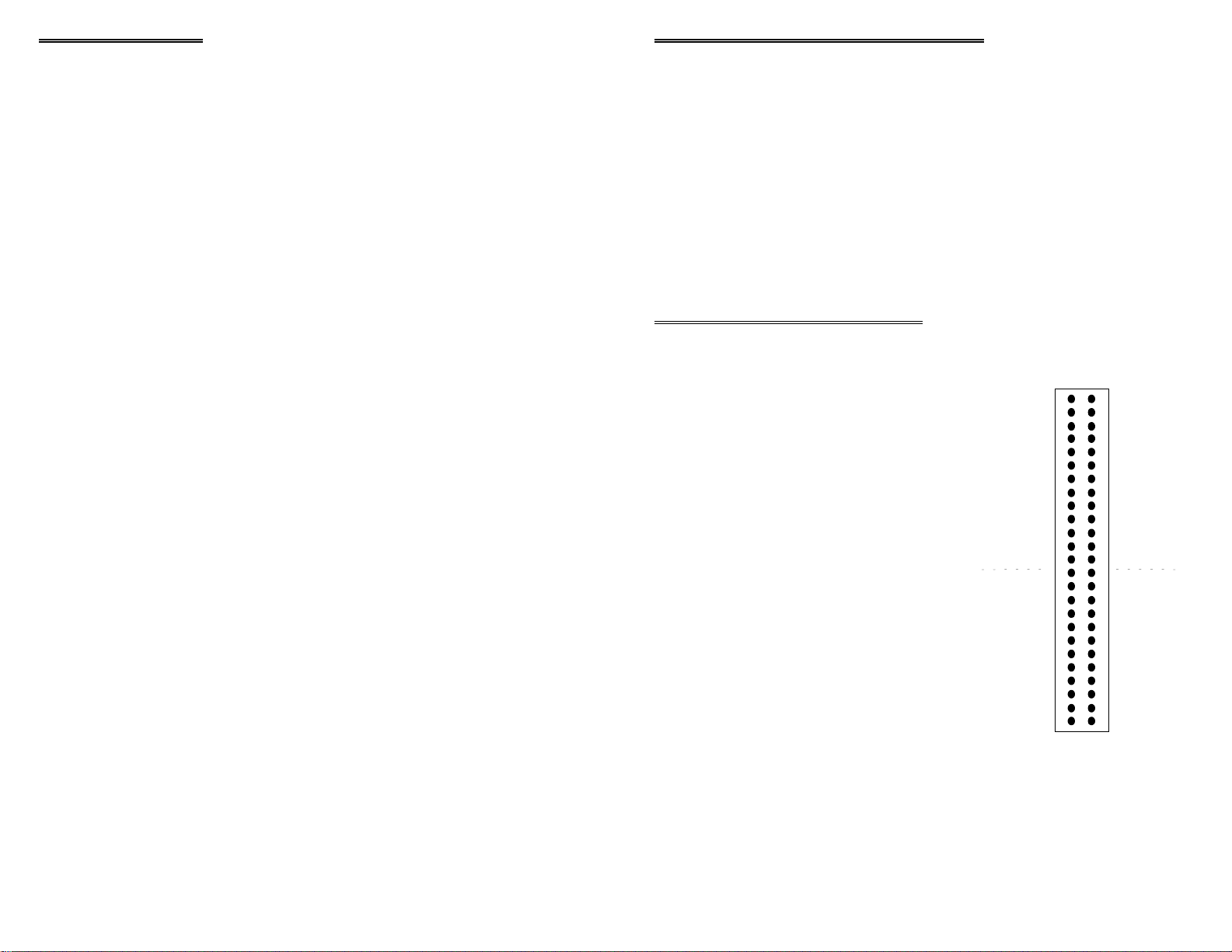
CONNECTOR DIAGRAM
The I/O connector for each of these boards is a
50 pin header connector accessible from the
rear of the PC through the expansion
backplate. The signals available are direct
connections to an 82C55 digital I/O chip.
The connector accepts female 50 pin header
connectors, such as those on the C50FF-2, 2
foot cable with connectors.
If frequent changes to signal connections or
signal conditioning is required, please refer to
the information on the CIO-TERM100, CIOSPADE50 and CIO-MINI50 screw terminal
boards.
BASE + 0, 8, 16, 24BASE + 4, 12, 20, 28
GND
C0
C2
C4
C6
B0
B2
B4
B6
A0
A2
A4
A6
C0
C2
C4
C6
B0
B2
B4
B6
A0
A2
A4
A6
50
48
46
44
42
40
38
36
34
32
30
28
26
24
22
20
18
16
14
12
10
8
6
4
2
49
47
45
43
41
39
37
35
33
31
29
27
25
23
21
19
17
15
13
11
9
7
5
3
1
+5V
C1
C3
C5
C7
B1
B3
B5
B7
A1
A3
A5
A7
C1
C3
C5
C7
B1
B3
B5
B7
A1
A3
A5
A7
15
8
Page 11
ARCHITECTURE
SPECIFICATIONS
82C55 CONTROL & DATA REGISTERS
Each CIO-DIO is composed of 82C55 parallel I/O chips. Each chip contains 3 data
and one control register occupying 4 consecutive I/O locations. The number of I/O
locations occupied by a CIO-DIO board is equal to 4 times the number of 82C55
chips on the board.
The first address, or BASE ADDRESS, is determined by setting a bank of switches on
the board.
A register is easy to read and write to.
The register descriptions follow the format shown below:
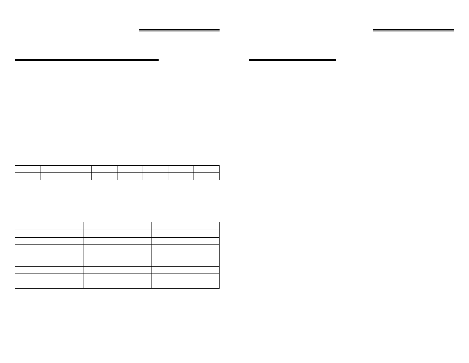
01234567
A0A1A2A3A4A5A6A7
Where the numbers along the top row are the bit positions within the 8 bit byte and the
numbers and symbols in the bottom row are the functions associated with that bit.
To write to or read from a register in decimal or HEX, the following weights apply:
HEX VALUEDECIMAL VALUEBIT POSITION
110
221
442
883
10164
20325
40646
801287
POWER CONSUMPTION
CIO-DIO48
+5V Supply 150 mA typical / 220 mA max.
+12V Supply None.
-12V Supply None.
CIO-DIO48H
+5V Supply 700 mA typical / 800 mA max.
+12V Supply None.
-12V Supply None.
CIO-DIO96
+5V Supply 190 mA typical / 320 mA max.
+12V Supply None.
-12V Supply None.
CIO-DIO192
+5V Supply 380 mA typical / 600 mA max.
+12V Supply None.
-12V Supply None.
NOTE
Additional power will be drawn by user's connections to the power
pins accessible on CIO-DIO connectors.
To write a control word or data to a register, the individual bits must be set to 0 or 1
then combined to form a Byte. Data read from registers must be analyzed to determine which bits are on or off.
9
14
Page 12
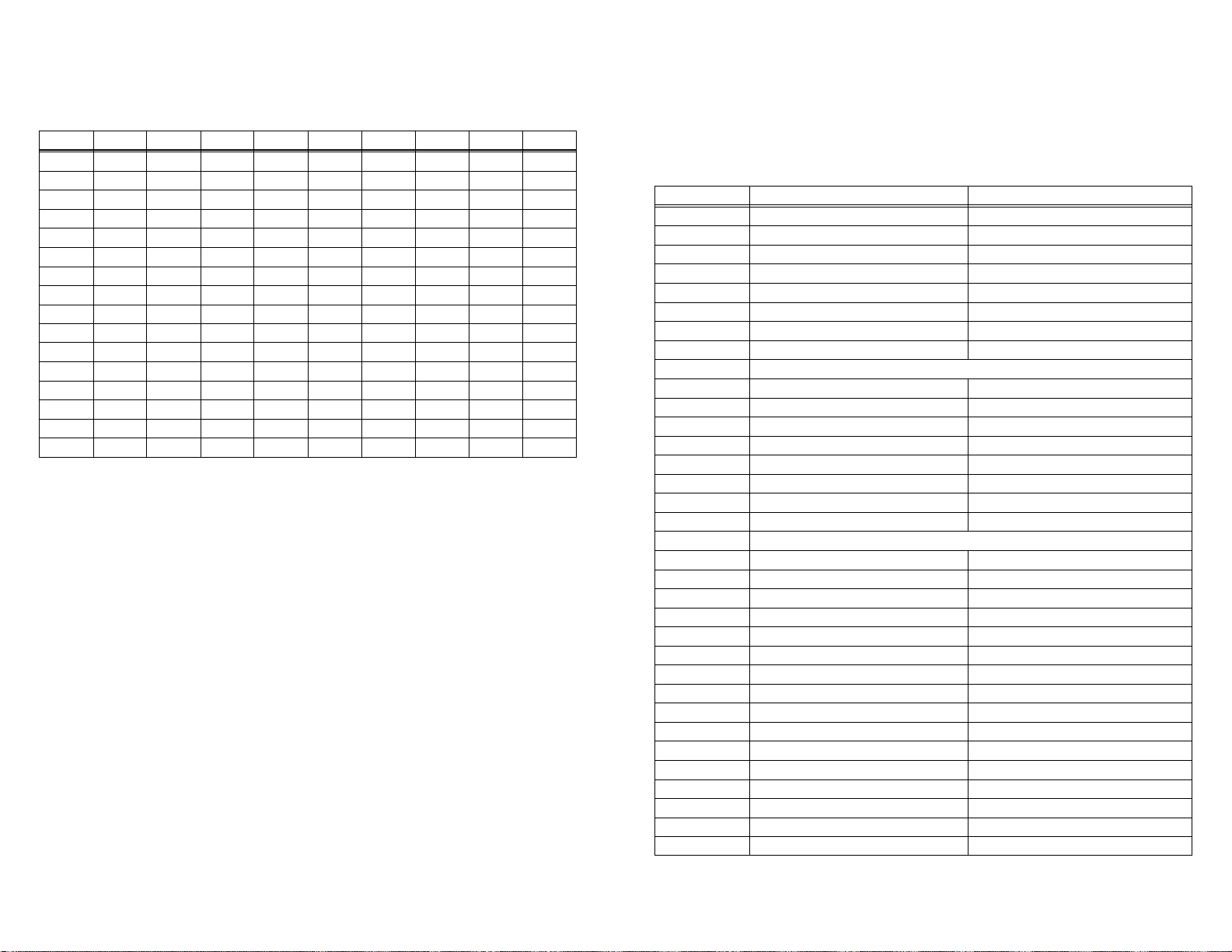
The two groups of ports, group A and group B, may be independently programmed in
one of several modes. The most commonly used mode is mode 0, input / output
mode. The codes for programming the 82C55 in this mode are shown below. D7 is
always 1 and D6, D5 & D2 are always 0.
CLBCUADECHEXD0D1D3 D4
OUTOUTOUTOUT128800000
INOUTOUTOUT129811000
OUTINOUTOUT130820100
ININOUTOUT131831100
OUTOUTINOUT136880010
INOUTINOUT137891010
OUTININOUT1388A0110
INININOUT1398B1110
OUTOUTOUTIN144900001
INOUTOUTIN145911001
OUTINOUTIN146920101
ININOUTIN147931101
OUTOUTININ152980011
INOUTININ153991011
OUTINININ1549A0111
ININININ1559B1111
The method of programming required to set/read bits from bytes is beyond the scope
of this manual. It will be covered in most Introduction To Programming books, available from a bookstore.
In summary form, the registers and their function are listed on the following table.
Within each register are 8 bits which may constitute a byte of data or 8 individual bit
set/read functions.
WRITE FUNCTIONREAD FUNCTIONADDRESS
Port A OutputPort A Input of 82C55BASE + 0
Port B OutputPort B InputBASE + 1
Port C OutputPort C InputBASE + 2
Configure 82C55None. No read back on 82C55BASE + 3
Port A OutputPort A Input of 82C55BASE + 4
Port B OutputPort B InputBASE + 5
Port C OutputPort C InputBASE + 6
Configure 82C55None. no read back on 82C55BASE + 7
ADDITIONAL CIO-DIO96 & 192 ONLY
Port A OutputPort A Input of 82C55BASE + 8
Port B OutputPort B InputBASE + 9
Port C OutputPort C InputBASE + 10
Configure 82C55None. No read back on 82C55BASE + 11
Port A OutputPort A Input of 82C55BASE + 12
Port B OutputPort B InputBASE + 13
Port C OutputPort C InputBASE + 14
Configure 82C55None. no read back on 82C55BASE + 15
ADDITIONAL CIO-DIO 192 ONLY
Port A OutputPort A Input of 82C55BASE + 16
Port B OutputPort B InputBASE + 17
Port C OutputPort C InputBASE + 18
Configure 82C55None. No read back on 82C55BASE + 19
Port A OutputPort A Input of 82C55BASE + 20
Port B OutputPort B InputBASE + 21
Port C OutputPort C InputBASE + 22
Configure 82C55None. no read back on 82C55BASE + 23
Port A OutputPort A Input of 82C55BASE + 24
Port B OutputPort B InputBASE + 25
Port C OutputPort C InputBASE + 26
Configure 82C55None. No read back on 82C55BASE + 27
Port A OutputPort A Input of 82C55BASE + 28
Port B OutputPort B InputBASE + 29
Port C OutputPort C InputBASE + 30
Configure 82C55None. No read back on 82C55BASE + 31
13
10
Page 13
82C55 DIGITAL I/O REGISTERS
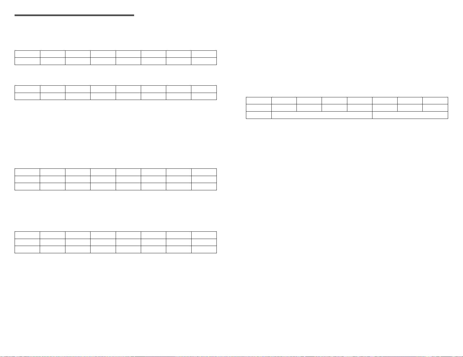
In 82C55 mode 0 configuration, ports configured for output hold the output data written. The output byte may be read back by reading a port configured for output.
PORT A DATA
BASE ADDRESS +0
01234567
A0A1A2A3A4A5A6A7
PORT B DATA
BASE ADDRESS +1
01234567
B0B1B2B3B4B5B6B7
Ports A & B may be programmed as input or output. Each is written to and read from
in Bytes, although fo r control and monitor ing purposes the individua l bits are more
interesting.
Bit set/reset and bit read functions require that unwanted bits be masked out of reads
and ORed into writes.
PORT C DATA
BASE ADDRESS +2 (8-bit mode)
01234567
C1C2C3C4C5C6C7C8
CL1CL2CL3CL4CH1CH2CH3CH4
Port C may be used as one 8 bit port of either input or output, or it may be split into
two 4 bit ports which may be independently input or output.
INPUT PORTS
In 82C55 mode 0 configuration, ports configured for input read the state of the input
lines at the moment the read is executed, transitions are not latched.
For information on modes 1 (strobed I/O) and 2 (bi-directional strobed I/O), you will
need to acquire an Intel or AMD data book and see the 82C55 data sheet.
82C55 CONTROL REGISTER
BASE ADDRESS +3
01234567
CLB M1CUAM2M3MS
Group BGroup A
The 82C55 may be programmed to operate in Input/ Output (mode 0), Strobed Input/
Output (mode 1) or Bi-Directional Bus (mode 2).
Included here is information on programming the 82C55 in mode 0. Those wishing to
use the 82C55 in modes 1 or 2, must procure a data book from Intel Corporation Literature Department.
When the PC is powered up or RESET, the 82C55 is reset. This places all 24 lines in
Input mode and no further programming is needed to use the 24 lines as TTL inputs.
To program the 82C55 for other modes, the following control code byte must be
assembled into on 8 bit byte.
PORT C DATA
BASE ADDRESS +2 (4-bit mode)
01234567
C1C2C3C4C5C6C7C8
CL1CL2CL3CL4CH1CH2CH3CH4
The notation for the upper 4 bit port is PCH3-PCH0, and for the lower, PCL3-PCL0.
Although it may be split, every read and write to port C carries 8 bits of data so
unwanted information must be ANDed out of reads, and writes must be ORed with the
current status of the other port.
OUTPUT PORTS
11
Group A FunctionM2M3
Input / OutputMode 000
Strobed Input / OutputMode 110
Bi-DirectionalMode 2X1
Independent FunctionCHCLBA
Input1111
Output0000
M1 = 0 is mode 0 for group B. Input / Output
M1 = 1 is mode 1 for group B. Strobed Input / Output
The Ports A, B, C High and C Low may be independently programmed for input or
output.
12
 Loading...