

Page 1
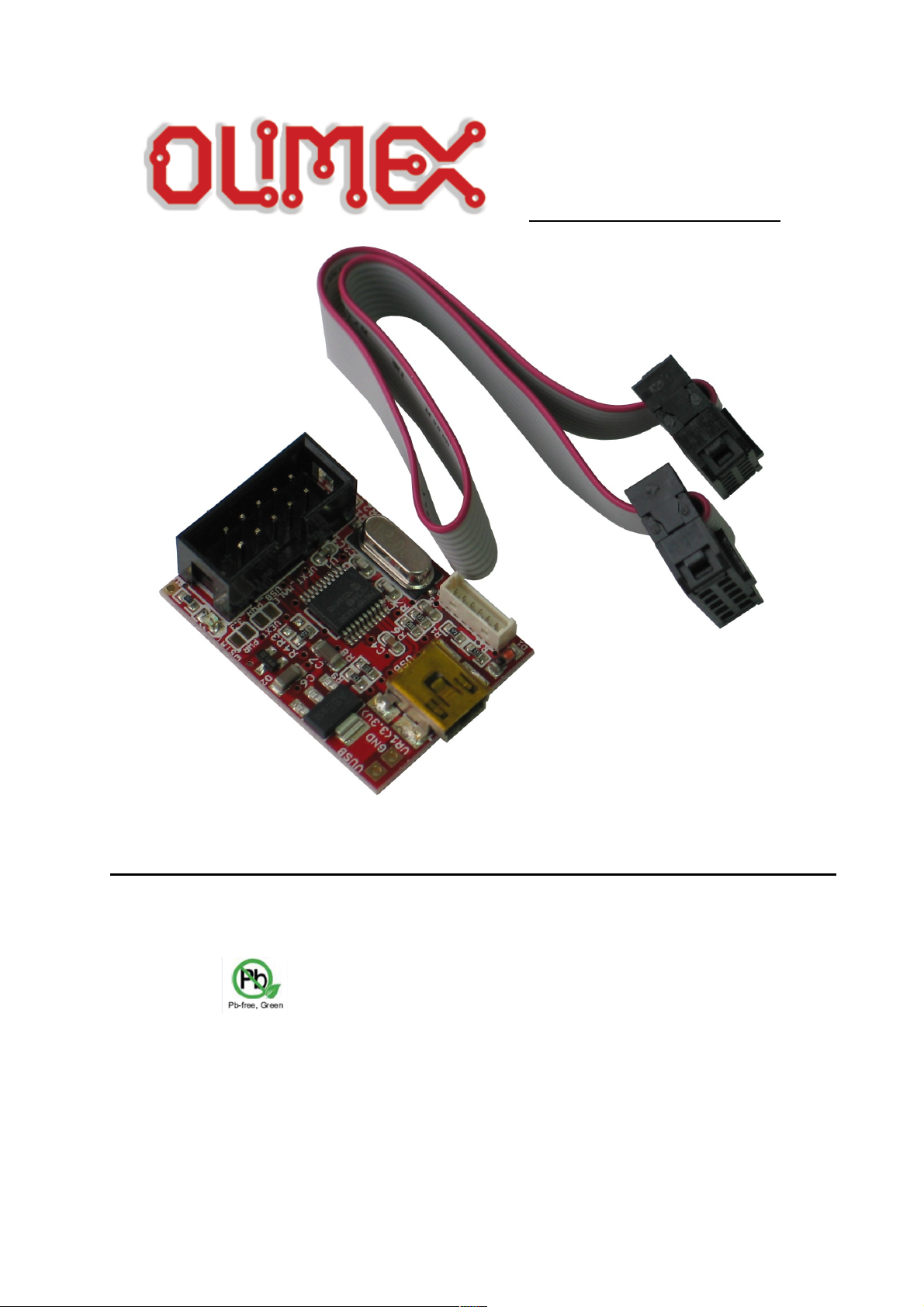
MOD-USB-RS232 development board
Users Manual
All boards produced by Olimex are ROHS compliant
Revision Initial, May 2011
Copyright(c) 2011, OLIMEX Ltd, All rights reserved
Page 1
Page 2

INTRODUCTION:
MOD-USB-RS232 is module board with PIC18F14K50 microcontroller. It is
a simple USB to UART converter that features UEXT. It can be used to add Virtual
Com Port to other Olimex's module, or development board, with UEXT, but
without Com Port. The board can be configured in both device and host mode, depending on jumpers 3_RX/3_TX and 4_TX/4_RX (see Jumper Description below).
For using MOD-USB-RS232 with some of our modules, it's jumpers has to be
configured for host mode. For using MOD-USB-RS232 with some of our
development boards, it's jumpers has to be configured for device mode.
BOARD FEATURES:
• MCU: PIC18F14K50 20-Pin USB Flash Microcontrollers with nanoWatt
XLP Technology.
• mini USB connector
• status led
• male UEXT connector plus 10 pin cable for it
• RESET circuit
• FR-4, 1.5 mm, red soldermask, component print
• Dimensions: 35.70 x 25.83 mm (1.41 x 1.02")
ELECTROSTATIC WARNING:
The MOD-USB-RS232 board is shipped in protective anti-static packaging. The
board must not be subject to high electrostatic potentials. General practice for
working with static sensitive devices should be applied when working with this
board.
BOARD USE REQUIREMENTS:
Cables: The cable you will need depends on the programmer you use. If you use
PIC-ICD2-POCKET, or PIC-Kit3, you will need USB A-B cable. For PIC-ICD2TINY, you will need RS232 cable. For PIC-ICD2, you will need USB A-B cable, or
RS232 cable. You will need adapter PIC-ICSP for programming, because the
board's ICSP connector is not Microchip's standard connector, it is a mini type one.
Hardware: Programmer PIC-ICD2-POCKET, PIC-ICD2, PIC-ICD2-
TINY, PIC-Kit3, or other compatible programming tool.
Software: MPLAB IDE
Note: This microcontroller does not support debug functionality.
Page 2
Page 3

PROCESSOR FEATURES:
MOD-USB-RS232 board use USB Flash microcontroller PIC18F14K50 from
MICROCHIP Technology Inc. with these features:
− Flash Program Memory (words): 8k
− SRAM (bytes): 512
− Universal Serial Bus Features:
− USB V2.0 Compliant SIE
− Low Speed (1.5 Mb/s) and Full Speed (12 Mb/s)
− Supports Control, Interrupt, Isochronous and Bulk Transfers
− Supports up to 16 Endpoints (8 bidirectional)
− 256-Byte Dual Port RAM (DPRAM) for USB
− On-Chip USB Transceiver
− Flexible Oscillator Structure:
− Four Crystal modes, including High-Precision PLL for USB
− Two External Clock modes, up to 48 MHz
− EC Low, Medium, and High-Power modes
− Internal 31 kHz Oscillator
− HF-INTOSC 16 MHz
− Secondary Oscillator using Timer1 @ 32 kHz
− Fail-Safe Clock Monitor:
− Allows for safe shutdown if any clock stops
− Peripheral Features:
− Three Programmable External Interrupts
− Seven Interrupt-on-Change (IOC) Configurable for Rising, Falling or
Both Rising/Falling Edge Detection
− One Enhanced Capture/Compare/PWM (ECCP) module with Auto-
Shutdown and PWM Steering
− Master Synchronous Serial Port (MSSP) module supporting SPI mode,
and I2C. mode with Address Mask Capability
− Enhanced Universal Synchronous Asynchronous Receiver Transmitter
(EUSART) module:
− Supports RS-485, RS-232 and LIN compatibility
− Auto-wake-up on Start bit
− Auto-Baud Detect
Page 3
Page 4

− Analog Features:
− 2 Analog Rail-to-Rail Comparator modules with:
− Programmable rail-to-rail reference voltage (% of VDD) or 1.024V
(nominal) band gap reference
− Comparator inputs and outputs externally accessible
− SR Latch mode
− 10-Bit, 9-Channel Analog-to-Digital (A/D) Converter module
− Special Microcontroller Features:
− Power-on Reset (POR)
− Power-up Timer (PWRT) and Oscillator Start-up Timer (OST
− Programmable Brown-out Reset (BOR)
− Software enable feature
− Configurable shutdown in Sleep
− Low/high-power configurable
− Four selectable trip points
− Self-Reprogrammable under Software Control
− Programmable Code Protection
− Single-Supply In-Circuit Serial Programming. (ICSP.) via Two Pins
− Operating Voltage Range of 1.8V to 5.5V
− Priority Levels for Interrupts
− Low-Power, High-Speed CMOS Flash Technology
Page 4
Page 5
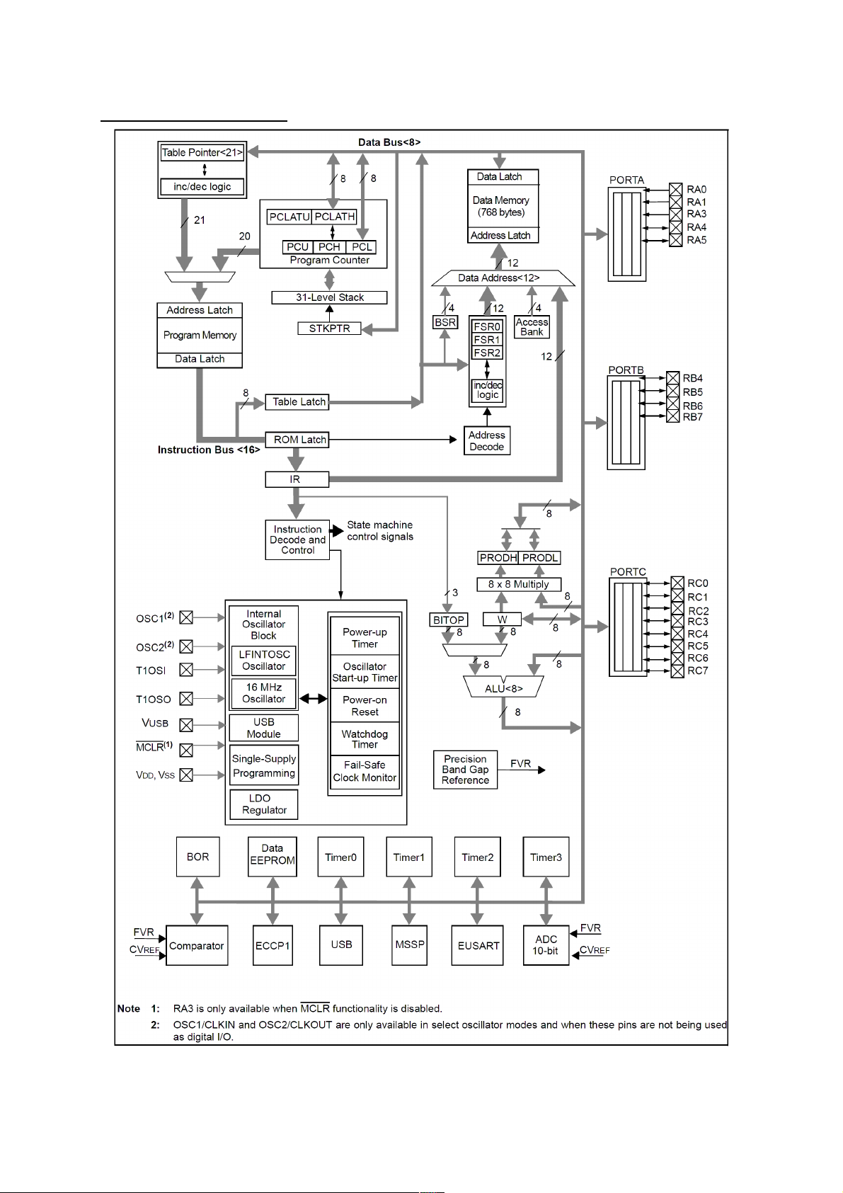
BLOCK DIAGRAM:
Page 5
Page 6

MEMORY MAP:
Page 6
Page 7

SCHEMATIC:
Page 7
1-2-close
1-2-close
10 0 nF
27 pF
27 pF
47 0 nF
10 nF
10uF/6.3V
10uF/6.3V
BZV 55C 8 V2
BAT54C
WU0 6S
12 MHz/ 20p F
4. 7k
33 R(N A)
33 R (N A)
4. 7k4. 7k
20 k
33 k
39 0 R/1%
24 0R/1%
56 0R
24 0R/1%
BH 10S
OPEN
MIC R O_B
OP EN
3. 3V
3. 3V
3. 3V
3. 3V
3. 3V
3. 3V
3. 3V
3. 3V
LM 111 7 IMP X- AD J
#S S
#S S
D+ /P GD
D+ /P GD
D+ /P GD
D- /P GC
D- /P G C
D- /P GC
MIS O
MIS O
MO SI
MO SI
RS T
RS T
RX D
RX D
RX D
RX D
SC K
SC K
SC L
SC L
SD A
SD A
STA T
STA T
TXD
TXD
TXD
TXD
US B_ D ETECT
US B_ DETE CT
US B_ POW ER
US B_ POW ER
US B_ VBU S
VPP
1
2
3
3_RX/3_TX
1
2
3
4_TX/ 4_RX
C1
C2
C3
C4
C5
C6
C7
D1
D2
GN D
12345
6
IC SP
Q1
R1
R2
R3
R4R5
R6
R7
R8
R9
R1 0
R1 1
STA T
RA0/D+/P GD
19
RA1/D-/P GC
18
RA3/MCLR/VP P
4
RA4/AN3/OSC2/CLK OUT
3
RA5/OS C1/CLKIN
2
RB4/AN10/SDI/SDA
13
RB5/AN11/RX/DT
12
RB6/S CK/SCL
11
RB7/TX /CK
10
RC0/AN4/C12IN+/INT0/V REF+16RC1/AN5/C12IN1-/INT1/V REF-
15
RC2/AN6/P1D/C12IN2-/C VREF /INT2
14
RC3/AN7/P 1C/C12IN3-/PGM
7
RC4/P1B/C12O UT/SRQ
6
RC5/CCP1/P 1A/T0CKI
5
RC6/AN8/SS /T13CKI/T1OSCI
8
RC7/AN9/SD O/T1OS CO
9
VDD
1
VSS
20
VUS B
17
U1
PIC1 8F1 4K 50- I/SS
1 2
3 4
5 6
7 8
9 10
UE XT_M AL E
12
UEXT_PWR_E
D+
D-
GND
GND1
GND2
GND3
GND4
ID
VB US
US B
1 2
US B_ PW R_3 .3
ADJ/G ND
IN OUT
VR 1(3 .3 V)
VU SB
MOD-USB-RS232
Re v. A
CO PYRIG HT (C ) 2 01 0, O LIME X Lt d.
ht tp ://www .o lim ex .c om/d e v
USB
POWER SUPPLY
UEXT
ICSP
USB
LED STAT
Page 8

BOARD LAYOUT:
POWER SUPPLY CIRCUIT:
MOD-USB-RS232 can take power from two sources:
5 VDC via pin holes VUSB and GND.
5 VDC via USB connector.
The programmed board power consumption is about 20 mA with all peripherals
enabled
RESET CIRCUIT:
MOD-USB-RS232 reset circuit includes R1 (4.7k), R11(240Ω/1%), D1
(BZV55C8V2), PIC18F14K50 pin 4 (RA3/MCLR/VPP).
CLOCK CIRCUIT:
Quartz crystal 12 MHz is connected to PIC18F14K50 pin 2
(RA5/OSC1/CLKIN) and pin 3 (RA4/AN3/OSC2/CLKOUT).
Page 8
Page 9

JUMPER DESCRIPTION:
USB_PWR_3.3
This jumper, when is closed, connects PIC18F14K50 pin 17 (VUSB) – signal
USB_VBUS, to VCC (3.3V).
Default state is opened.
UEXT_PWR_3.3
This jumper, when is closed, connects UEXT pin 1 to VCC (3.3V). When MOD-USBRS232 is used in host mode – this jumper must be closed, because the other module
will be power supplied via MOD-USB-RS232.
Default state is opened.
3_RX/3_TX
This jumper, when is in position 3_RX, connects UEXT pin 3 to PIC18F14K50 pin 12
(RB5/AN11/RX/DT). When this jumper is in position 3_TX, connects UEXT pin 3 to
PIC18F14K50 pin 10 (RB7/TX/CK).
Default state is 3_RX shorted.
4_TX/4_RX
This jumper, when is in position 4_TX, connects UEXT pin 4 to PIC18F14K50 pin 10
(RB7/TX/CK). When this jumper is in position 4_RX, connects UEXT pin 4 to
PIC18F14K50 pin 12 (RB5/AN11/RX/DT).
Default state is 4_TX shorted.
In default state jumpers 3_RX/3_TX and 4_TX/4_RX are configured for device
mode.
INPUT/OUTPUT:
Status Led (red) with name STAT connected to PIC18F14K50 pin 14
(RC2/AN6/P1D/C12IN2-/CVREF/INT2).
Page 9
Page 10

EXTERNAL CONNECTORS DESCRIPTION:
UEXT:
Pin # Signal Name
1 VCC
2 GND
3 RXD
4 TXD
5 SCL
6 SDA
7 MISO
8 MOSI
9 SCK
10 #SS
USB
Pin # Signal Name
1 USB_POWER
2 D-/PGC
3 D+/PGD
4 Not Connected
5 GND
Page 10
Page 11

MECHANICAL DIMENSIONS:
Page 11
Page 12

AVAILABLE DEMO SOFTWARE:
USB to UART converter with Windows drivers for Serial Port
Page 12
Page 13

ORDER CODE:
MOD-USB-RS232 - assembled and tested board
How to order?
You can order to us directly or by any of our distributors.
Check our web www.olimex.com/dev for more info.
Revision history:
Board's Revision: Rev. A, created May 2010
Manual's revision: Rev. Initial, created May 2011
Page 13
Page 14

Disclaimer:
© 2011 Olimex Ltd. All rights reserved. Olimex®, logo and combinations thereof, are registered
trademarks of Olimex Ltd. Other terms and product names may be trademarks of others.
The information in this document is provided in connection with Olimex products. No license, express
or implied or otherwise, to any intellectual property right is granted by this document or in
connection with the sale of Olimex products.
Neither the whole nor any part of the information contained in or the product described in this
document may be adapted or reproduced in any material from except with the prior written
permission of the copyright holder.
The product described in this document is subject to continuous development and improvements. All
particulars of the product and its use contained in this document are given by OLIMEX in good faith.
However all warranties implied or expressed including but not limited to implied warranties of
merchantability or fitness for purpose are excluded.
This document is intended only to assist the reader in the use of the product. OLIMEX Ltd. shall not
be liable for any loss or damage arising from the use of any information in this document or any error
or omission in such information or any incorrect use of the product.
Page 14
 Loading...