OKIDATA 3320, 3321 Troubleshooting Manual

MICROLINE 3320/3321
Troubleshooting Manual
with Components Parts List
All specifications are subject to change without notice.

HP, LaserJet and PCL5e are trademarks of Hewlett-Packard Co.

PREFACE
This manual describes in detail troubleshooting of the component parts for Microline
320/321 TURBO printer and provides a parts list.

TROUBLESHOOTING MANUAL

CONTENTS
1. OUTLINE ...................................................................................................1
2. TOOLS ......................................................................................................5
3. TROUBLESHOOTING TABLES ...............................................................5
4. TROUBLESHOOTING FLOWCHART ......................................................7
5. CIRCUIT DIAGRAM
6. COMPONENT PARTS LIST
1. OUTLINE
This troubleshooting flowchart has been prepared for the repair of each board assembly of the
Microline 320/321 TURBO printer. The repairmen using this manual are assumed to be familiar
with certain techniques.
1.1 Items to Check Before Repair
• Check the inspection items specified in the instruction manual.
• Find out as many details of the trouble as possible from the customer.
• Inspect in the conditions as close as possible to those at the time the trouble occurred.
• Proceed with the repair as follows:
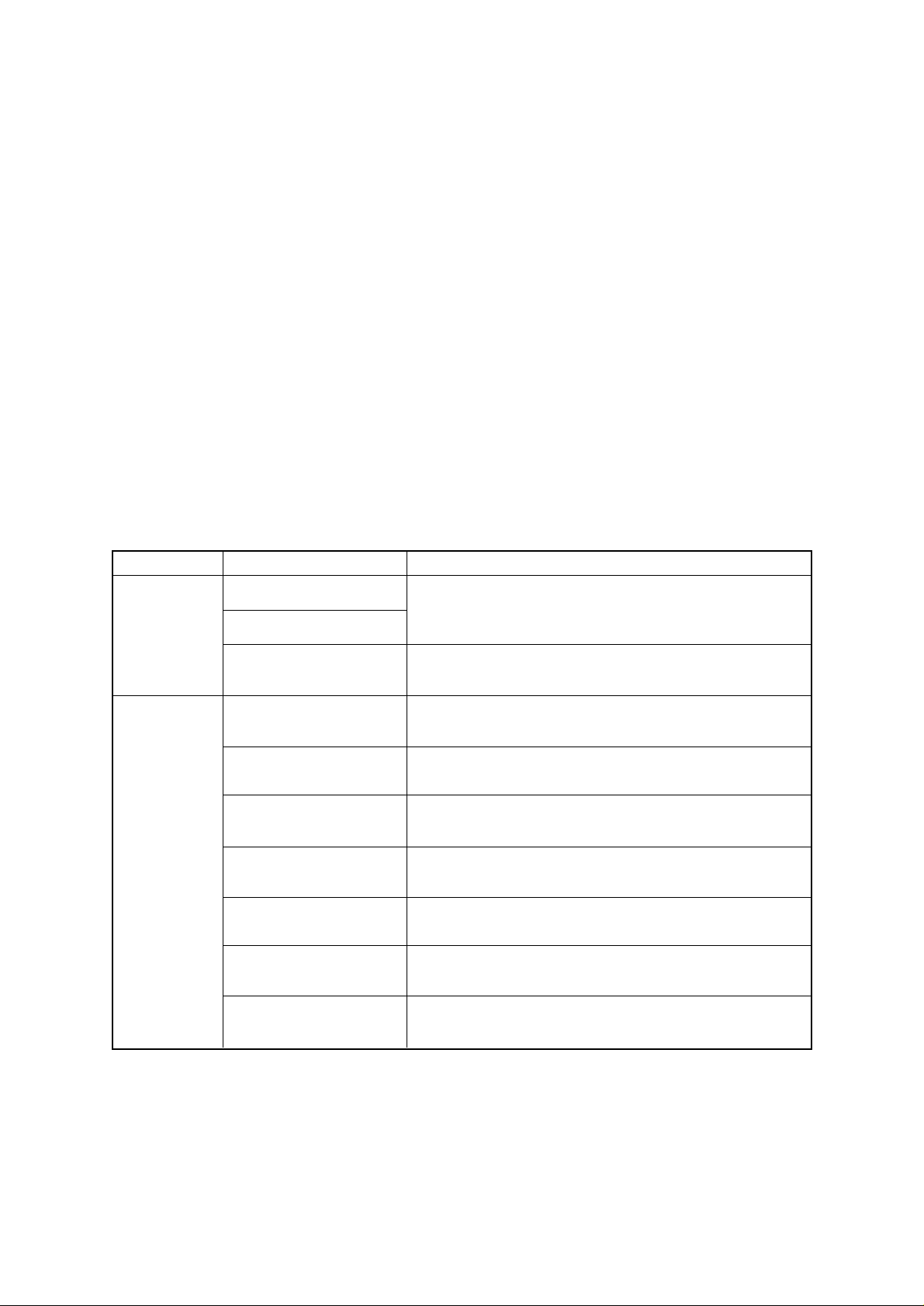
Check the trouble status according to Table 1.1 for the details of the trouble. Then, locate the
trouble position according to the detailed flowchart.
• Carry out a thorough test after the repair to check for correct functioning.
1.2 Troubleshooting
Trouble contents Surmise of troublleStatus
Table 1.1
Trouble upon
power on
Trouble
during
printing
Power is not supplied
No spacing operation
Homing does not end
normally
Paper jam while paper
insertion
Smearing/Missing dots
Faint or dark print
Ribbon feed trouble
Line feed trouble
Malfunction of switch on
operation panel.
Data receiving failure
Transformer, Power & Control Board, Driver Board, Operation Panel.
Space motor, carriage Cable, Print Head.
Space Motor, Carriage Cable, Spacing Mechanism, Driver Board
Pressure roller Mechanism, Support Protector, Pull up roller cover.
Print Head, Power & Control Board, Space Motor, Carriage Cable,
Driver Board
Print Head, Ribbon feed assembly, Power & Control Board, Driver
Board
Ribbon feed assembly, Space motor, Power & Control Board, Driver
Board
LF motor, Platen assy, LF mechanism, Power & Control Board, Driver
Board
Operation Panel, Power & Control Board, Driver Board
Power & Control Board, (I/F/P.C.B), I/F Cable, Menu setting, Driver
Board
Note: Refer to the Maintenance Manual for the troubleshooting flow chart of this table.
- 1 -
1.3 Lamp Display
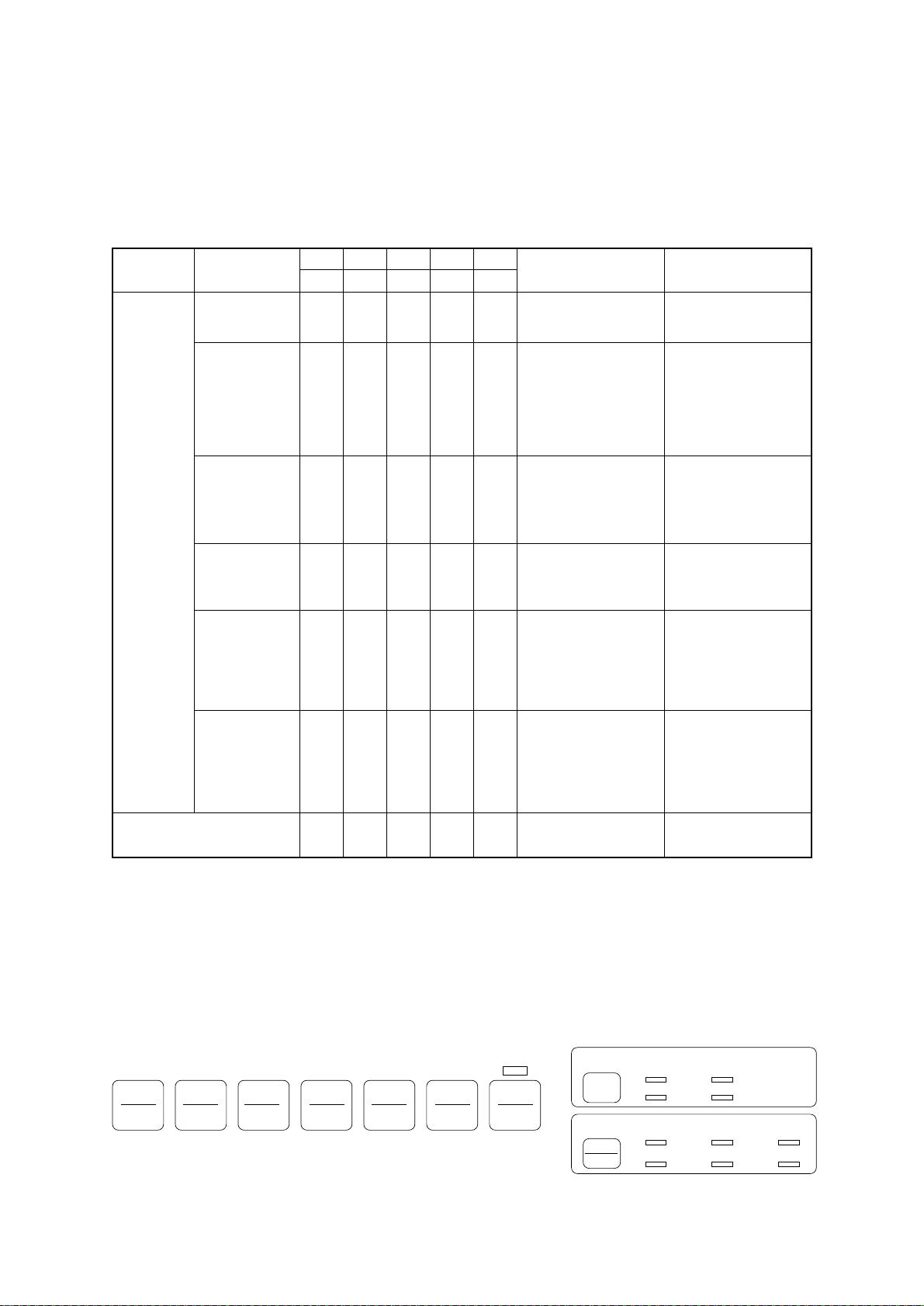
(1) Printer mode display
Table 1.2
ALARM
CATEGORY
OPERATOR
ALARM
ALARM CONTENTS TROUBLESHOOTING
Paper end
alarm
Paper
change lever
alarm
ALARM MENU 10 CPI 15 CPISEL
ON
—
ON
OFF
—
—
—
BLINK
1
—
From, cut sheet or
bottom paper end
OFF
Change lever is set to
TOP position while
paper is already inserted
from rear or bottom.
Set New paper.
• Set the lever to
specified position.
• Check rear sensor
lever.
• Replace Power &
Control Board.
Paper jam alarm
Print Head
thermal alarm
ON
OFF
OFF
—
—
BLINK
1
OFF
—
BLINK
• Cut sheet could not be
1
ejected.
• Cut sheet could not be
fed properly.
—
Print head temperature
exceeds 119°C.
• Remove the paper or
check feed
Mechanism.
• Press SEL key.
• Wait until it is cooled.
• Replace P.H. or Power
& Control Board.
Space motor
thermal alarm
OFF
—
BLINK
1
—
—
Temperature of space
motor and driver
exceeds specified value.
• It is recovered
automatically.
• Replace SP motor or
Power &Control
Board.
LF motor
temperature
OFF
—
BLINK
1
alarm
FATAL ALARM
BLINK
OFF
OFF
2
Note: BLINK 1: 400 ms ON, 400 ms OFF
BLINK 2: 200 ms ON, 200 ms OFF
— : LED is kept in Current Condition (no change)
(2) Fault alarm display
When the printer detects any of the various alarm states, the information is displayed as
shown below on the operation panel. The alarm is specified by lamp combination of PRINT
QUALITY and CHARACTER PITCH. (See Table 1.3 for details.)
SEL
SEL
MENU
EXIT
POWERALARM
SHIFT
LF
Micro Feed
Down
GROUP ITEM SET
FF/LOAD
Micro Feed
Up
TEAR PARK QUIET
MENU
—
PRINT
—
Temperature of LF
motor and driver
exceeds specified value.
Hardware Alarm has
occurred.
TOF
• It is recovered
automatically.
• Replace LF motor or
Power & Control
Board.
See Table 1.3.
PRINT QUALITY
CHARACTER PITCH
RESET
HSD UTILITY
NLQ SSD
10
17
12
20
15
PROP
- 2 -
REMARKS TROUBLESHOOTING
Table 1.3 (1/2)
LED DISPLAY
Replace Power & Control Board
Replace ROM or Power & Control
Board
Read/write error
Check sum error
Replace Power & Control Board
Read/write error
Replace Power & Control Board
No reaction when MPU
reads data
Turn the power OFF and ON or
replace Power & Control Board
Replace Power & Control Board
Replace ROM or Power & Control
Board
Replace I/F Board
MPU is locked up and it is
reset after 65 ms.
NMI port of MPU is kept
low level.
FFFF data is detected
due to MPU locked up.
Read/write error
Replace I/F Board
Replace I/F board or Power & Control
Replace ROM on I/F Board or
I/F Board
Read/write error
Check sum error
Board
: LED Blink (200 ms ON, 200ms OFF)
No reaction from serial I/F
Board
: LED Lights up.
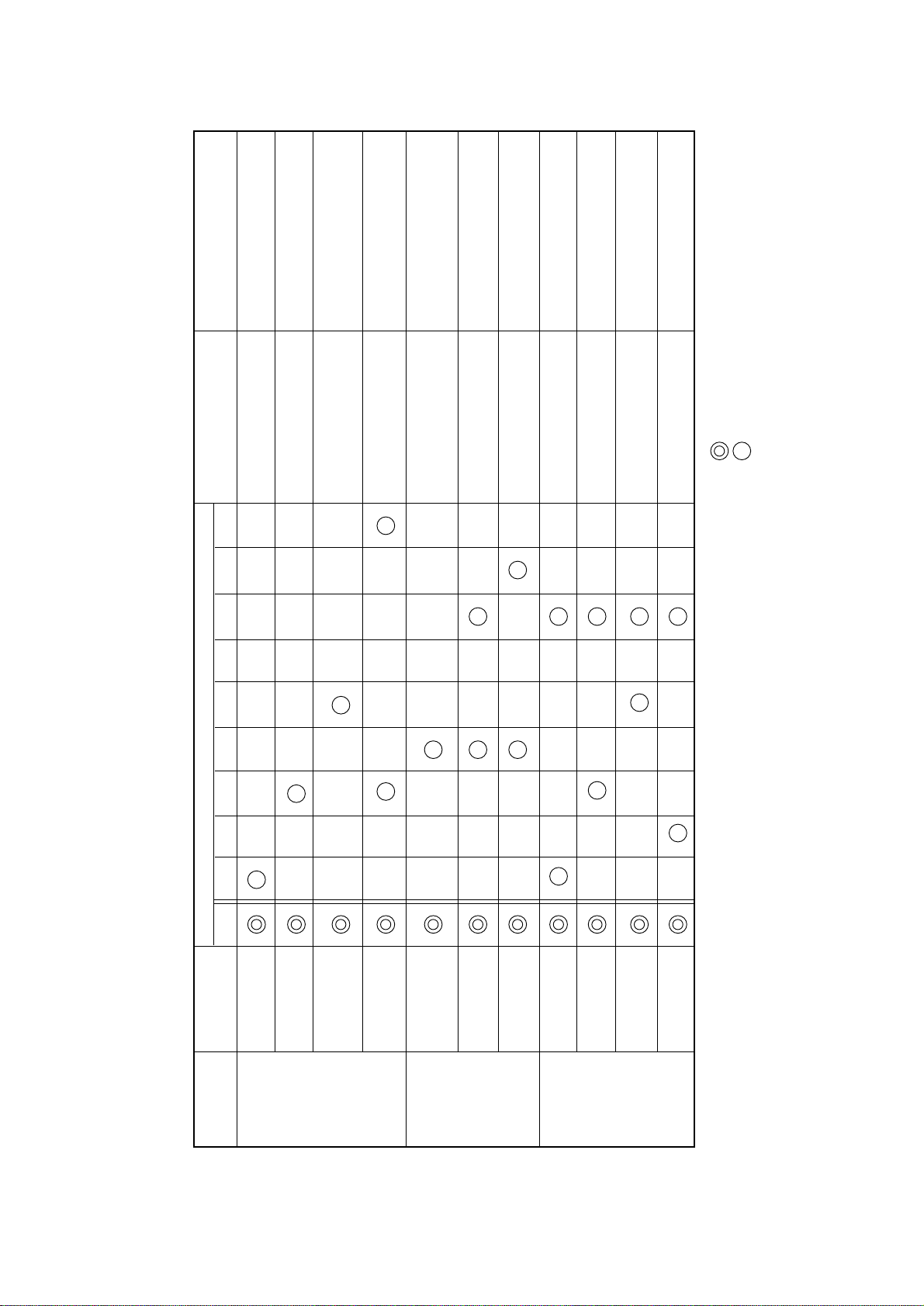
(3) Fatal Alarm
ALARM 10 12 15 17 20 PROP HSD UTL NLQ
ALARM
ALARM
CATEGORY
MPU internal
RAM alarm
Program
ROM alarm
RAM on
MAIN
CONTROL
Control Board
alarm
EEPROM
alarm
ALARM
WDT (Watch
Dog Timeout)
alarm
FIRMWARE
DETECTION
- 3 -
NMI signal
alarm
BRK instruction
ALARM
alarm
MPU internal
RAM alarm
ROM alarm
SERIAL
RAM on I/F
board alarm
INTERFACE
ALARM
I/F not
mounted
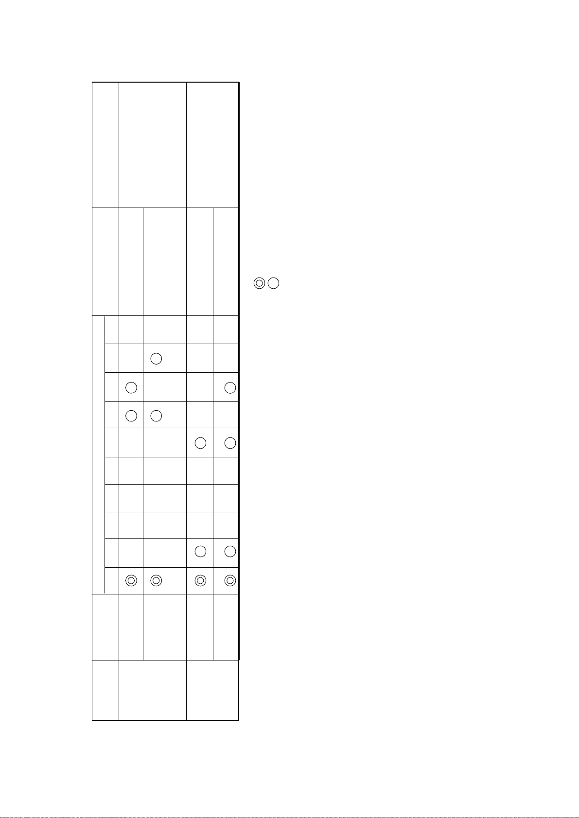
• Replace space motor.
REMARKS TROUBLESHOOTING
Space IPT is not occurred
Table 1.3 (2/2)
LED DISPLAY
• Replace P.H. cable.
• Replace Power & Control Board.
• Replace Driver Board.
• Check the mechanism if
load is too much.
• Check the P.H. connection.
• Replace Print Head.
• Replace P.H. cable.
within in specified timing.
Print head does not reach
to the home position.
Thermister is open, short
with 0V or short with +5V.
• Replace Driver Board.
: LED Blink (200 ms ON, 200ms OFF)
: LED Lights up.
ALARM 10 12 15 17 20 PROP HSD UTL NLQ
ALARM
ALARM
CATEGORY
Spacing alarm
Print Head
mounting alarm
SPACING
ALARM
PRINT HEAD
A/D alarm
Print Head
PRINT HEAD
ALARM
Gap AD alarm
- 4 -

2. TOOLS
In addition to the general maintenance tools, the following are necessary:
– Oscilloscope : Approx. 100 MHz or more
– Soldering iron : Standard (A soldering iron with a thin tip is best.)
3. TROUBLESHOOTING TABLES
1 The power source can not be turned on.
2 Only the POWER lamp lights. (The printer does not work.)
3 The printer alarm is displayed.
3-1 Printer Internal RAM Alarm
3-2 S-I/F Internal RAM Error
3-3 S-I/F Connection Alarm
3-4 Program ROM Alarm
3-5 S-I/F ROM Alarm
3-6 EEPROM Alarm
3-7 WDT Alarm, BRK Command Alarm
3-8 NMI Alarm
3-9 Printer External RAM Alarm
3-10 S-I/F External RAM Alarm
3-11 SPACING Alarm, HOMING Alarm
3-12 Head A/D Alarm
3-13 Head Gap A/D Alarm
4 Wrong characters are printed or some characters are not printed.
5 Defective line feed.
6 When pressing the operation switch, it does not work.
6-1 The SEL switch does not work.
6-2 The SHIFT switch does not work.
6-3 The LF switch does not work.
6-4 The FF switch does not work.
6-5 The TEAR switch does not work.
6-6 The PARK switch does not work.
6-7 The QUIET switch does not work.
6-8 The PRINT QUALITY switch does not work.
6-9 The CHARACTER PITCH switch does not work.
- 5 -

7 DATA can not be received.
7-1 Parallel interface data can not be received.
7-2 When receiving with the parallel interface, printed data is skipped, or the printer
does not work.
- 6 -

4 TROUBLESHOOTING FLOWCHART
1 The power source can not be turned on. (The POWER lamp does not light.)
• Check the connection between Transformer and Power & Control Board and Driver
Board and Operation panel.
• No Be sure the connection.
▼
• Yes Is Fuse (F1) on Filter PCB blown out?
• Yes Replace Fuse (F1).
▼
• No Are the signal level between 1-pin and 8-pin of CN1 on Power & Control Board,
29 Vac, between 3-pin and 6-pin, 8 Vac, and between 4-pin and 5 pin, 10 Vac?
• No Replace Transformer.
▼
• Yes Is the voltage level at VCC (1-pin) of Q6 of the Power & Control Board, +8V?
• No Is fuse (F1) on Power & Control Board blown out?
• Yes Replace Fuse (F1)?
▼
• No Replace D6, D7, D8 and D9 of the Power & Control Board.
▼
• Yes Is the voltage level between one side and the other of C25 of the Power &
Control Board, +5V?
• No Replace Q6 or TR6 of the Power & Control Board.
▼
• Yes Is +5V supplied for CN3 of the Driver board?
+5V (CN3 – 3 pin)
0V (CN3 – 2 pin)
• No Check +5V supplied for the Driver board or replace Driver board?
▼
• Yes Is +5V supplied for CN1 of the operation panel board?
+5V (CN1 – 5 pin)
0V (CN1 – 6 pin)
• No Replace a cable in the operation panel or replace the operation panel.
▼
• Yes Replace D2 or R2 on the operation panel.
- 7 -
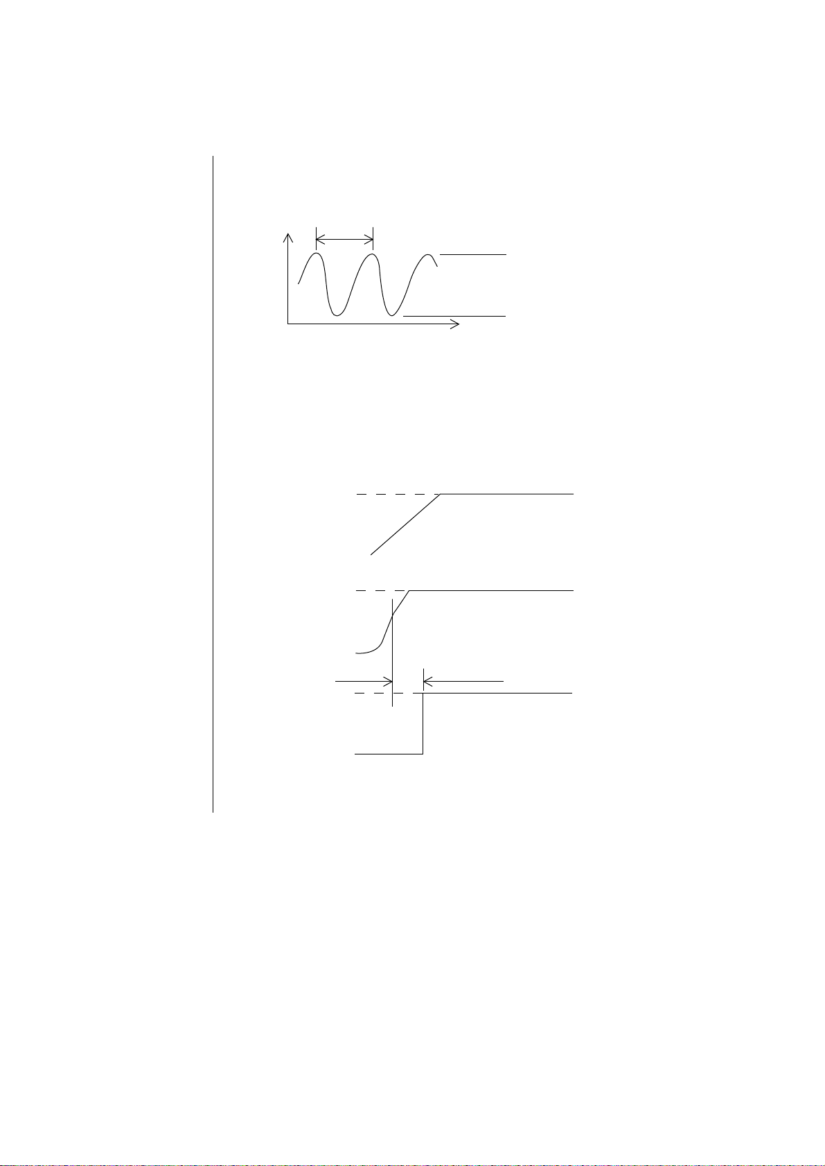
2 Only the POWER lamp lights. (The printer does not work.)
• Does the oscillating waveform from OSC of the Power & Control Board have the form
shown in Figure 1 below?
81.4 ns
V
(V)
T(ns)
+4 V ~ +5 V
0 V ~ 1V
Fig. 1
• No Replace OSC of the Power & Control Board.
▼
• Yes Does the RST-N signal have the waveform shown in Figure 2 below (with
+5 V and +8V signals as reference)?
+8 V
+8 V
0
+5 V
+5 V
0
+5 V
RST-N
0
Fig. 2
▼
• No If RS232C PCB is available, replace the RS232C PCB.
If the RS232C PCB is not available, replace the Power & Control
Board.
- 8 -
▼
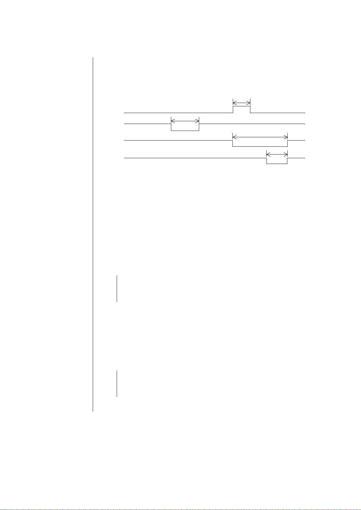
• Yes Do bus line signals of 4C (67 x 640) of the Power & Control Board such as ALEP, PSEN-N, LSICS-N and RDN/WRL-N have waveforms as shown in Fig. 4?
62 ms
ALE-P
102 ms
PSEN-N
203 ms
LSICS-N
76 ms
RD-N/WRL-N
+5V
0V
+5V
0V
+5V
0V
+5V
0V
Fig. 4
At the rising edge of PSEN-N and RD-N/WRL-N, the bus line level is decisively
set to “H” or “L”.
• No Replace Q501 of the Power & Control Board.
▼
• Yes Does the OPCLK-N/OPTXD signal arrive at CN1 of the operation panel?
See Fig. 5.
OPCLK-N (CN1-3 pin)
OPTXQ (CN1-4 pin)
• No Is the flexible calbe of the operation panel connected without break?
• No Replace the flexible cable.
▼
• Yes Replace CN3 of the Driver Board.
▼
• Yes Does the OPRXD signal arrive at CN1 of the operation panel? See Fig. 5.
OPRXD (CN1-2 pin)
• No Replace IC1 of the operation panel.
▼
• Yes Does the OPRXD signal arrive at CN3 of the Driver Board? See Fig. 5.
• No Is the flexible cable of the operation panel connected without break?
• No Replace the flexible cable
▼
• Yes Replace CN3 of the Driver Board.
▼
• Yes Replace Q501 of the Power & Control Board.
- 9 -

OPTXD
DATA
DATA
+5V
0V
OPCLK-N
OPRXD
DATA
Fig. 5
DATA
+5V
0V
+5V
0V
- 10 -

3 The printer alarm is displayed.
3-1 Printer internal RAM alarm
• Replace Q501 of the Power & Control Board.
3-2 S-I/F internal RAM alarms.
• Replace Q3 of the LXHI board.
3-3 S-I/F connection alarm.
• Replace the LXHI board.
3-4 Program ROM alarm.
• Replace Q1 of the Power & Control Board (EPROM).
3-5 S-I/F ROM alarm.
• Replace Q3 of the LXHI board.
3-6 EEPROM alarm.
• Is the voltage of Q5-8pin +5V?
• No Check TR5 and TR7 and pattern on the Power & Control Board.
Correct pattern or replace parts.
▼
• Yes Do signals of Q501 of the Power & Control Board (67 x 640) such as EECLKP and EEDIN-P and EECS-P have the waveforms shown in Fig. 6?
• No Replace Q501 of the Power & Control Board.
▼
• Yes Do signals of Q5 of the Power & Control Board (EEPROM) such as EEDINP, EECS-P, EECLK-P and EEDOUT-P have the waveforms shown in Fig. 6?
• No Check EEDIN-P, EECS-P and EECLK-P patterns and parts
connected to the pattern. Correct pattern or replace parts.
▼
• Yes Replace Q501 of the Power & Control Board.
- 11 -
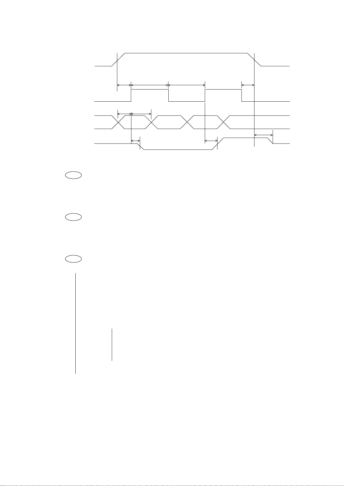
EECS-P
+5V
0V
EECLK-P
EEDIN-P
EEDOUT-P
MIN
50 ns
MIN
100 ns
MIN
450 ns
MIN
100 ns
MIN
500 ns
Fig. 6
3-7 WDT alarm, BRK command alarm
• Is the alarm canceled by turning on power?
• No Replace ROM, Q1 or the Power & Control Board.
3-8 NMI alarm
• Is the alarm canceled by turning on power?
MIN
450 ns
MIN
500 ns
MIN
0 ns
MIN
100 ns
+5V
0V
+5V
0V
+5V
0V
• No Replae Power & Control Board.
3-9 Printer external RAM alarm.
• Do signal of Q3, Q4 (DRAM) of the Power & Control Board such as RAS-N, CAS-N, OE,
WE have the waveforms shown in Fig. 7?
RAS-N (Q3, Q4-5)
CAS-N (Q3, Q4-16)
RD-N (Q3, Q4-1)
WRL-N (Q3, Q4-4)
• No Is the dumping resistance of each signal broken?
Check Q502 (Power & Control Board)?
• Yes Replace the dumping resistance or Q502
▼
• No
▼
• Yes Replace Q3, Q4.
- 12 -
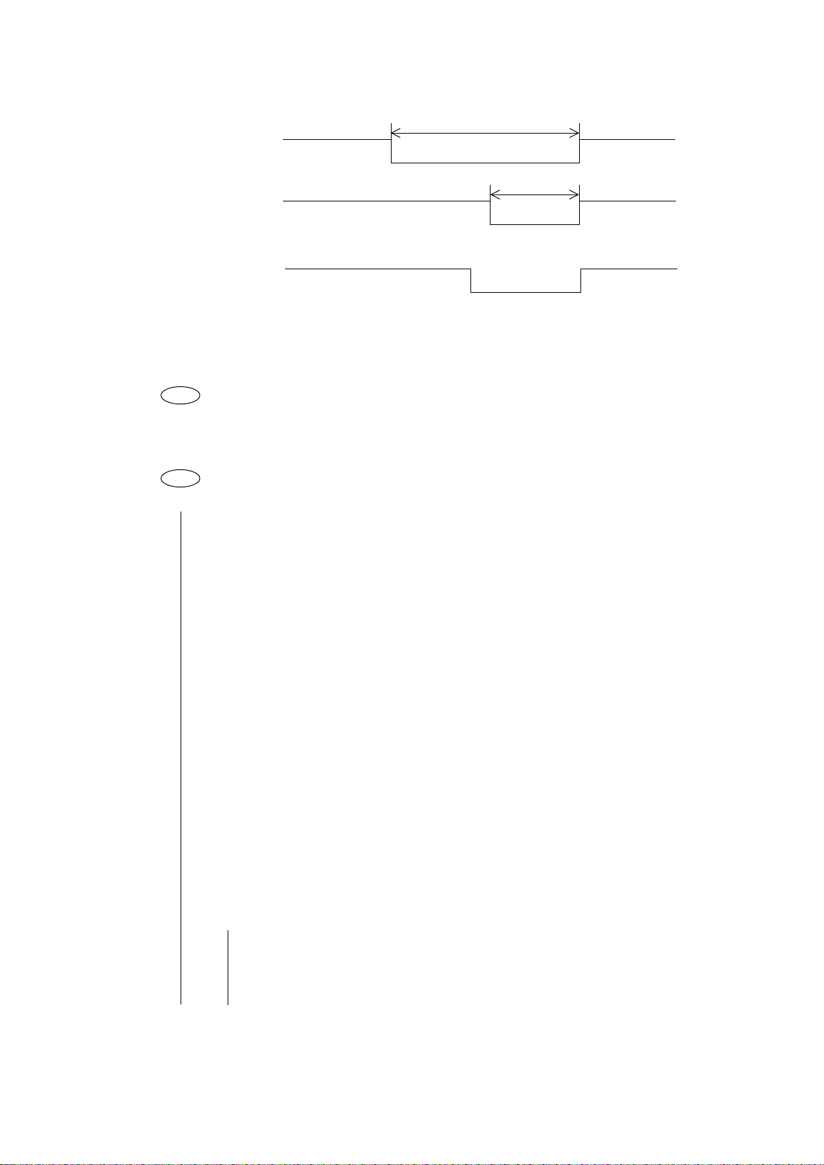
RAS-N
CAS-N
103 ns
41.4 ns
+5V
0V
+5V
0V
RD-N/WRH-N/WRL-N
At the rising edge of OE, WE, the bus line level is decisively set to “H” or “L”.
Fig. 7
3-10 S-I/F external RAM alarm.
• Replace Q9 of the LXHI board.
3-11 SPACING alarm, HOMING alarm
• Is the fuse (F1) on the Driver board blown?
• Yes Replace F1.
▼
• No Is VNF of MTDV (HA13412) short-circuited to U0, V0, or W0?
VNF (MTDV-11 pin)
U0 (MTDV-13 pin)
V0 (MTDV-15 pin)
W0 (MTDV-17 pin)
+5V
0V
• Yes Replace MTDV
▼
• No Do signals of SPU, SPV, SPW and SPD-A of MTDV have the wave forms shown in
Fig. 10?
• No Check patterns SPU, SPV, SPW between Q501 and MTDV. When they are
OK, replace the Driver PCB Q501.
▼
• Yes Do signals of U0, V0, and W0 of the MTDV have the wave forms shown in Fig. 10?
• No Replace the HTDV PCB.
▼
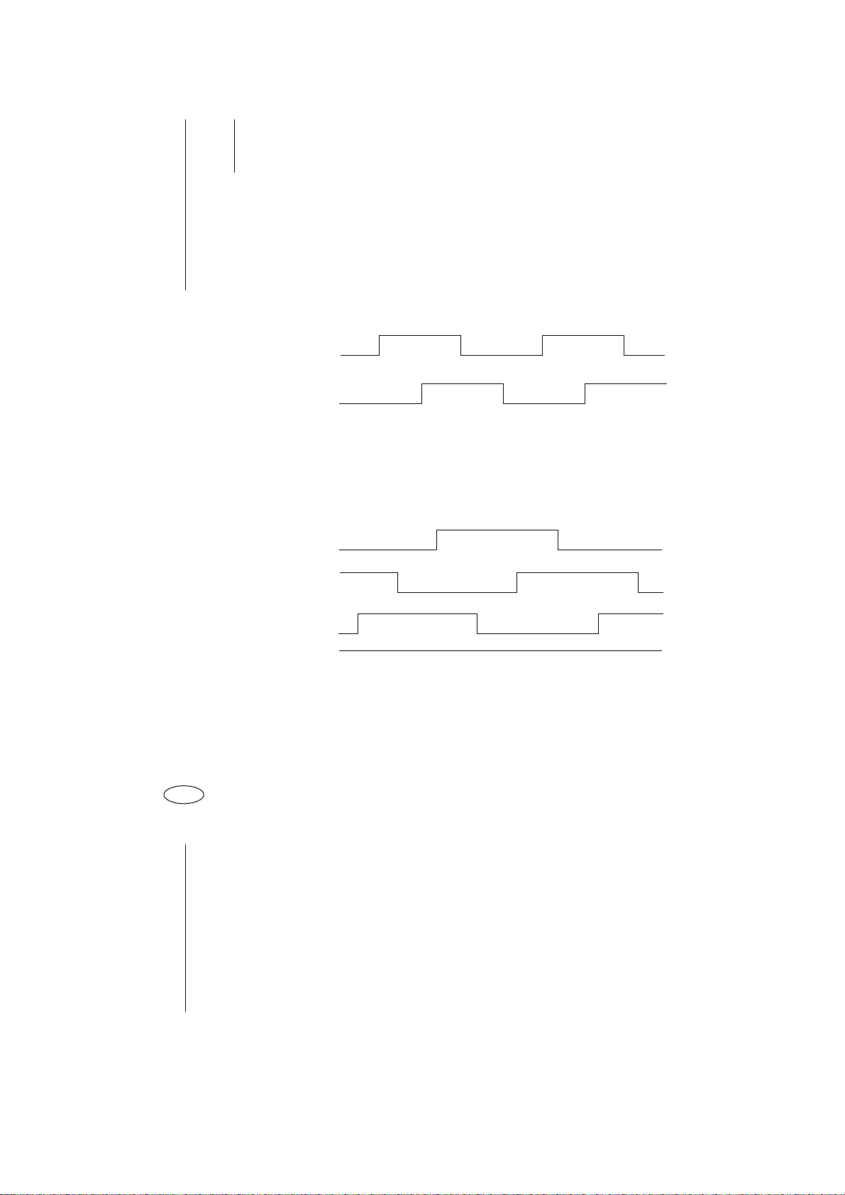
• Yes Do signals of PHASE A and PHASE B have the wave forms shown in Fig. 9?
• No Is the connection between CN5 on the Driver Board, and the CN on the
carriage are OK?
• No Secure the connection.
▼▼
• Yes Is there any disconnection of cable between the Driver Board and the
carriage?
- 13 -
• No Replace the Carriage.
▼
• Yes Replace the Cable.
▼
• Yes Do signals of PHASE A, PHASE B of Q501 have the wave forms shown in Fig. 9?
• No Check the parts and pattern between Q501 and CN6. Correct
pattern or replace parts.
▼
• Yes Replace Q501.
PHASE A
PHASE B
When the carriage is manually move.
Fig. 9
SPU
SPV
SPW
SPD-A
When the carriage is manually move.
+5V
0V
+5V
0V
+5V
0V
+5V
0V
+5V
0V
+5V
0V
Fig. 10
3-12 Head A/D alarm
• Is the voltage of the HTEMP-N signal of Q501 of the Power & Control Board (67 X 640) +5V?
HTEMP-N (Q501-62 pin)
• No Replace Q501.
▼
• Yes Is the connection of CN5 of the Driver Board secured?
• No Secure the connection of CN5.
▼
• Yes Replace the head.
- 14 -

3-13 Head Gap A/D alarm
• Is the voltage of HDGAP-N Signal of Driver Board CN5 22 pin +5V?
• Yes Replace the Head cable or the carriage.
▼
• No Replace the Power & Control Board.
- 15 -

4 Wrong characters are printed or some characters are not printed.
• Do signals of Q501 of the Power & Control Board (67 X 640) such as PSEN-N, LSICS-N,
RD-N, WRL-N, RAS-N and CAS-N have the wave forms shown in Figs. 4 and 7?
• No Replace Q501.
▼
• Yes Replace the head, Q501 of Driver board or the space motor.
- 16 -
5 Defective line feed.
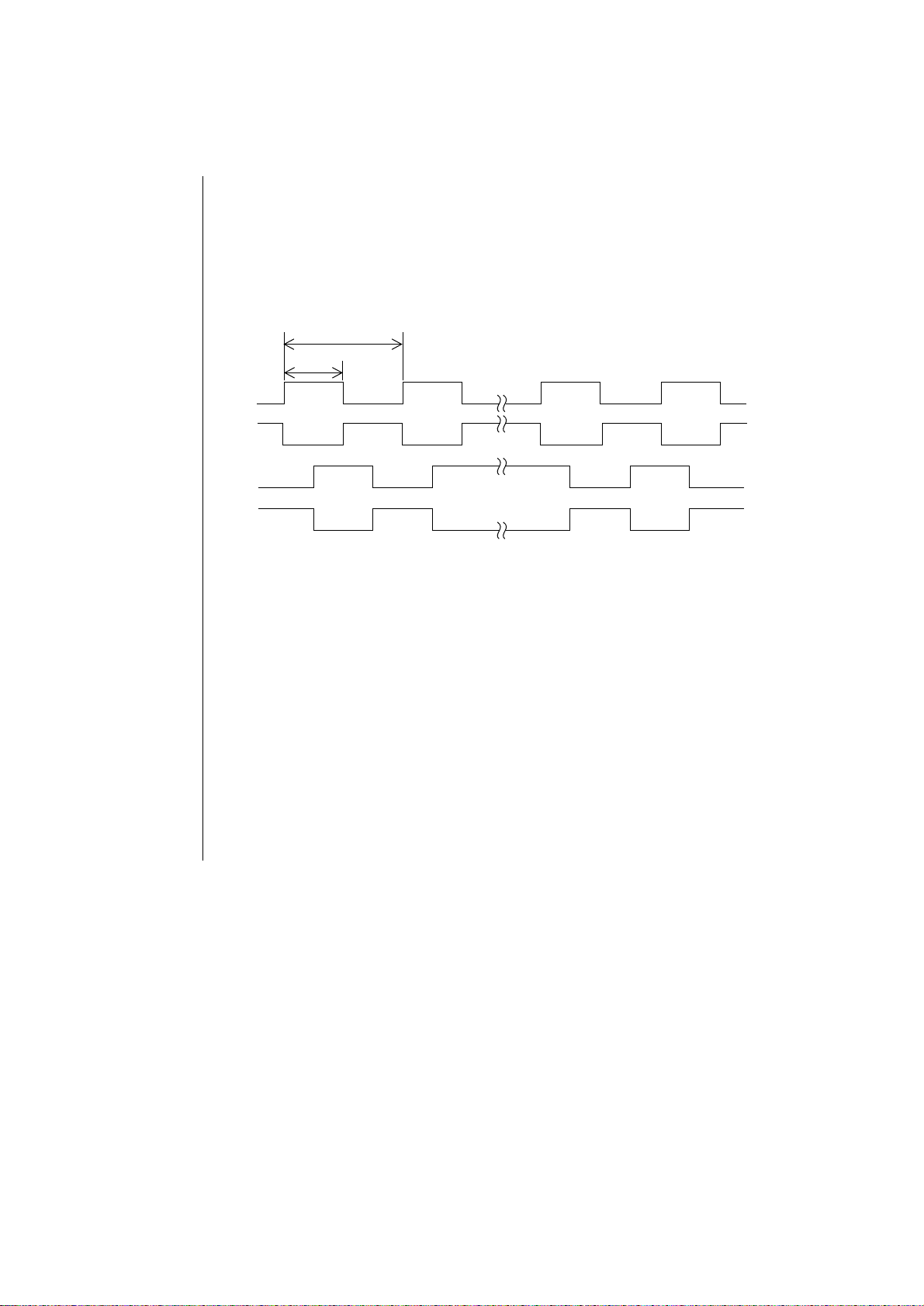
• Do signals of LFDV (Driver board) such as A1, A2, B1 and B2 have the waveforms shown
in Fig. 11?
A1 (LFDV-3 pin)
A2 (LFDV-7 pin)
B1 (LFDV-8 pin)
B2 (LFDV-12 pin)
4.44 ms
2.22 ms
A1
A2
+40V
0V
+40V
0V
B1
B2
Forward Reverse
Fig. 11
• No Replace LFDV.
LFDV (Driver Board)
When it does not work properly, replace Q501 or the Driver Board.
▼
• Yes Is the flexible cable connected without break?
• No Replace the flexible cable.
▼
• Yes Is the CN4 of the Driver Board broken?
• No Replace CN4
▼
• Yes Replace the LF motor.
+40V
0V
+40V
0V
- 17 -

6 The printer does not operate though the operation switch is pressed.
• Do the OPCLK-N and OPTXD signals arrive at CN3? See Fig. 5.
• No Replace Q501 of the Driver board.
▼
• Yes Do the OPCLK-N and OPTXD signals arrive at CN1 of the operation panel?
See Fig. 5.
• No Is the flexible cable of the operation panel connected without break?
• No Replace the flexible cable.
• Yes Replace CN3 of the Driver board.
▼
• Yes Does the OPRXD signal arrive at CN1 of the operation panel?
• No Replace IC1 of the operation panel.
▼
• Yes Does the OPRXD signal arrive at CN3 of the Driver board? See Fig. 5.
• No Is the flexible cable of the operation panel connected without break?
• No Replace the flexible cable.
• Yes Replace CN3 of the Driver board.
▼
• Yes Go to steps 6-1 to 6-9 .
6-1 SEL SW does not work.
• When SWC2 of IC1 (Bu5148S) is set to “L”, is SWI4 set to “L” by pressing SEL SW?
SWC2 (C1-7 pin)
SWI4 (IC1-3 pin)
• No Replace SEL SW.
▼
• Yes Replace IC1 or Q501 of the Driver board.
6-2 SHIFT SW does not work.
• When SWC2 of IC1 is set to “L”, is SWI3 set to “L” by pressing SHIFT SW?
SWI3 (IC1-10 pin)
• No Replace SHIFT SW.
▼
• Yes Replace IC1 or Q501 of the Driver board.
- 18 -

6.3 LF SW does not work.
• When SWC2 of IC1 is set to “L”, is SW1 set to “L” by pressing LF SW?
(IC1-18 pin)
SWI4 (ICI-3 pin)
• No Replace LF SW.
▼
• Yes Does LF SW recover IC1 or Q501 of the Driver board replaced?
• No Go to step 5.
6-4 FF SW does not work.
• When SWC2 of IC1 is set to “L”, is SWI2 set to “L” by pressing FF SW?
SWI2 (IC1-23 pin)
• No Replace FF SW.
▼
• Yes Does FF SW recover with IC1 or Q501 of the Driver board replaced?
• No Go to step 5.
6-5 TEAR SW does not work.
• When SWC1 of IC1 is set to “L”, is SWI4 set to “L” by pressing TEAR SW?
SWC1 (IC1-31 pin)
• No Replace TEAR SW.
▼
• Yes Does TEAR SW recover with IC1 or Q501 of the Driver board replaced?
• No Go to step 5.
6-6 PARK SW does not work.
• When SWC1 of IC1 is set to “L”, is SW2 set to “L” by pressing PARK SW?
• No Replace PARK SW.
▼
• Yes Does PARK SW recover with IC1 or Q501 of the Driver board replaced?
• No Go to step 5.
6-7 QUIET SW does not work.
• When SWC1 of IC1 is set to “L”, is SWI1 set to “L” by pressing QUIET SW?
• No Replace QUIET SW.
▼
• Yes Replace IC1 or Q501 of the Driver board.
- 19 -

6.8 PRINT QUALITY SW does not work.
• When SWC3 of IC1 is set to “L”, is SWI1 set to “L” by pressing PRINT QUALITY SW?
• No Replace PRINT QUALITY SW.
▼
• Yes Replace IC1 or Q501 of the Driver board?
6-9 CHARACTER PITCH SW does not work.
• When SWC1 of IC1 is set to “L”, is SWI3 set to “L” by pressing CHARACTER PITCH SW?
• No Replace CHARACTER PITCH SW.
▼
• Yes Replace IC1 or Q501 of the Driver board.
- 20 -
7 Data can not be received.
7-1 Parallel interface data can not be received.
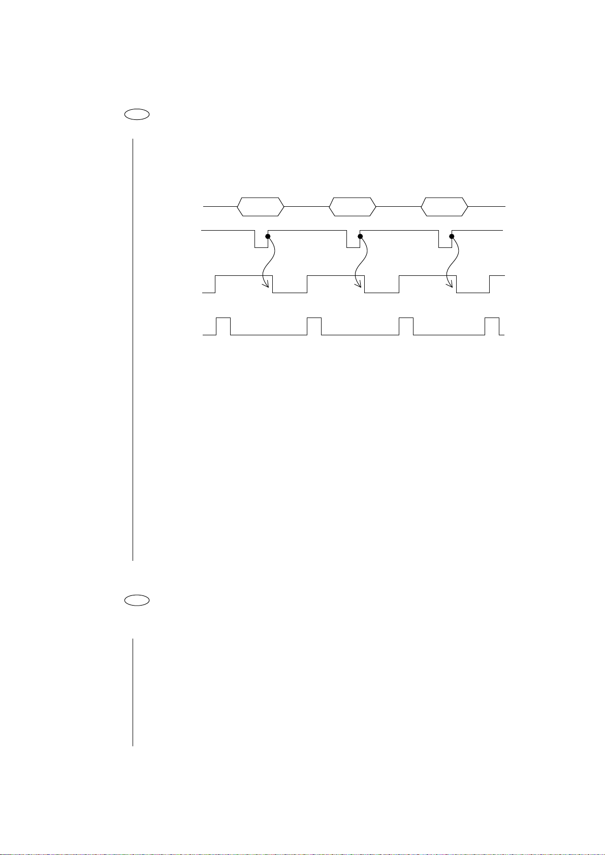
• Do the IFDATA 1 to 8 signals of Q501 of the Driver board have the waveform shown in Figure
12 below?
IFD1 ~ 8
STB-N
BUSY-N
ACK
Valid Valid Valid
Fig. 12
• No Replace either relative electric component to the DATA 1 to 8 signals, or
replace CN6 of the Driver board.
▼
• Yes Does the STB-N signal of Q501 have the waveform shown in Fig. 12?
• No Replace either resistor or capacitor of the STB-N signal.
▼
• Yes Do the BUSY-N and ACK signals have the waveforms shown in Fig. 12?
H
L
H
L
H
L
H
L
• No Replace Q501.
BUSY-N (Q501-64 pin)
ACK (Q501-63 pin)
▼
• Yes Replace Q3.
7-2 When receiving with the parallel interface, printed data is skipped, or the printer
does not work.
• Gap in the self-test?
• Yes To step 4.
▼
• No Does the signal of BUSY-N or ACK of Q501 of the Driver board have the waveform
shown in Figure 12?
• No Replace Q501.
▼
• Yes Replace either relative electric component to ACK or BUSY-N signal, or replace Q3
of the Driver board.
- 21 -

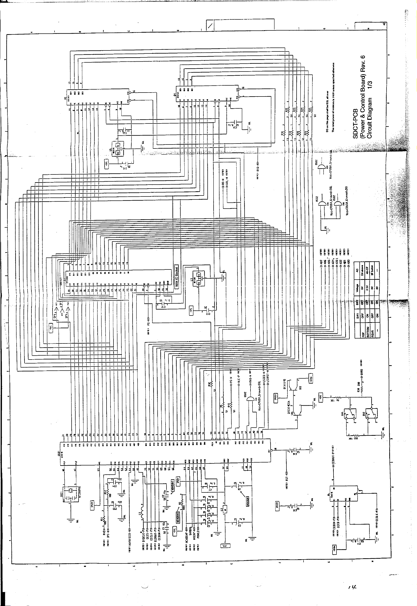
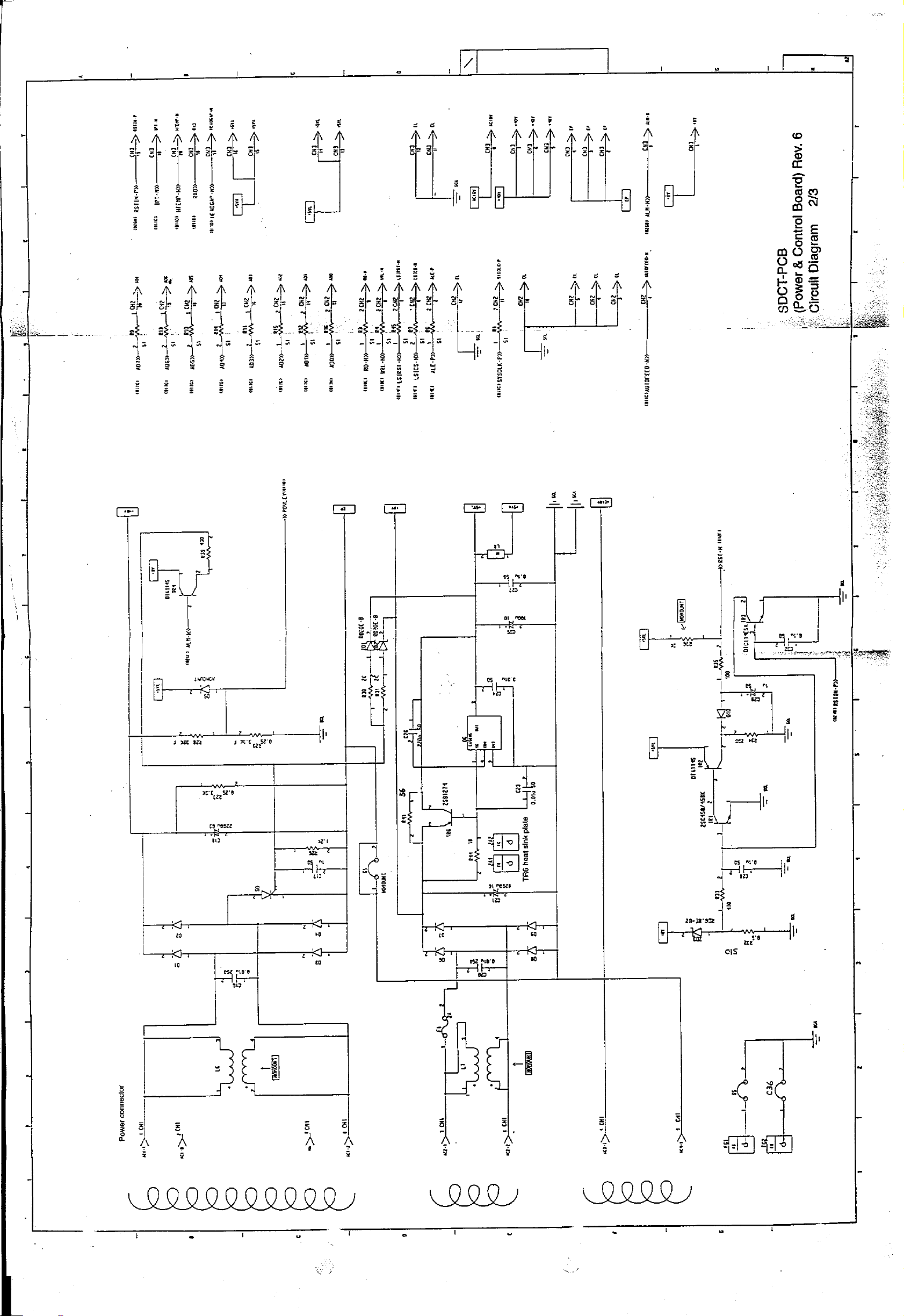
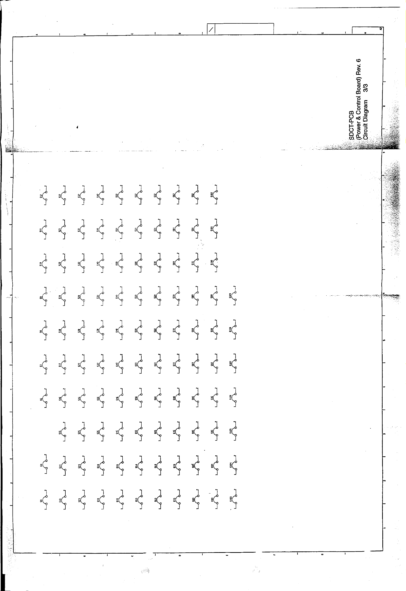
5. CIRCUIT DIAGRAM
SDCT-PCB (Power & Control Board) Rev. 6
SDDV-PCB (Driver Board) Rev. 4
LEOP-3 PCB (Operation Panel) Rev. 5 & 6
LXHI-PCB (Serial I/F Board) Rev. 7
Rev. 7
Rev. 8
Rev. 5
Rev. 6
Rev. 7
 Loading...