

Page 1

TF-300P
Field Service Manual
Ver. 02
July 8, 1999
TTIC
I
Page 2

Index
1. INTRODUCTION 1-1
1.1 STANDARD SPECIFICATIONS 1-1
1.2 GENERAL USER FUNCTION 1-6
1.3 GENERAL APPEARANCE 1-7
1.3.1 APPEARANCE 1-7
1.3.2 SHOW THE OPERATION PANEL 1-7
1.4 GENERAL MAINTENANCE FUNCTION 1-8
2. INSTALLATIONS 1-1
2.1 GENERAL 1-1
2.2 SITE SELECTION 1-2
2.3 UNPACKING 1-2
2.4 CHECK OF CONTENTS 1-3
2.5 INSTALLATION OF ATTACHMENTS 1-3
2.5.1 CARTRIDGE AND SIM CARD 1-3
2.5.2 HANDSET AND LINE CORD 1-3
2.5.3 AC CORD CONNECTION 1-4
2.5.4 LOADING PAPER 1-5
3. MAINTENANCE 3-1
3.1 ROUTINE INSPECTION 3-1
4. SYSTEM TEST 4-1
5. MECHANICAL DISASSEMBLY AND REASSEMBLY 5-1
5.1 GENERAL 5-1
5.1.1 PRECAUTIONS PARTS REPLACEMENT 5-1
5.1.2 TOOLS 5-1
5.2 GENERAL MECHANICAL STRUCTURE 5-2
5.3 HOW TO DISASSEMBLE AND REASSEMBLE 5-3
5.3.1 INSTALLING THE INK CARTRIDGE AND SIM CARD 5-3
5.3.2 AC PLUG, HANDSET AND DOC. SUPPORT 5-3
5.3.3 BOTTOM PLATE UNIT 5-3
5.3.4 SIM CARD HOLDER ASSEMBLY 5-4
5.3.5 SCANNER MODE UNIT 5-4
II
Page 3

5.3.6 SCANNER MODE ASM. 5-5
5.3.7 SCANNER UNIT 5-5
5.3.8 LOWER FRAME UNIT 5-5
5.3.9 UPPER FRAME UNIT. 5-6
5.3.10 DOCUMENT GUIDE ASSEMBLY 5-7
5.3.11 OPERATION PANEL UNIT 5-7
5.3.12 UPPER COVER UNIT 5-8
5.3.13 PRINTER MODE UNIT 5-8
5.3.14 PRINTER MODE ASM. 5-8
5.3.15 PAPER FEEDER UNIT 5-9
5.3.16 BASE FRAME UNIT 5-10
5.3.17 BOTTOM COVER UNIT 5-11
6. CIRCUIT DESCRIPTION 6-1
6.1 MAIN BOARD CIRCUIT 6-1
6.1.1 BLOCK DIAGRAM 6-1
6.1.2 INTEGRATED FAX CONTROLLER 6-1
6.1.3 SCANNER CONTROLLER 6-11
6.1.4 MOTOR DRIVERS 6-11
6.1.5 SWITCH AND SENSORS 6-11
6.1.6 BATTERY AND POWER DOWN RESET 6-11
6.1.7 FAX MODEM CIRCUIT 6-11
6.1.8 MEMORY 6-16
6.1.9 NETWORK INTERFACE 6-16
6.1.10 PANEL INTERFACE 6-16
6.2 PRINTER BOARD CIRCUIT DESCRIPTION 6-16
6.2.1 PRINTER BOARD TO INKJET HEAD INTERFACE 6-16
6.2.2 PAPER & CARRIAGE MOTOR 6-16
6.2.3 SENSORS & HOST CONNECTOR 6-16
6.2.4 PRINTER HEAD SUPPLY DETECT 6-16
6.2.5 MICROPROCESSOR AND MEMORY 6-16
6.3 KEY BOARD CIRCUIT DESCRIPTION 6-17
6.4 SIMCRAD BOARD CIRCUIT DESCRIPTION 6-17
6.5 NCU CIRCUIT DIAGRAM DESCRIPTION 6-17
6.5.1 GENERAL FUNCTIONS OF NCU (NETWORK CONTROL UNIT) CIRCUIT 6-17
6.5.2 DIALLING METHOD 6-17
6.5.3 RINGING DETECTION 6-18
6.5.4 FAX MESSAGE RECEIVING 6-18
III
Page 4

6.5.5 FAX MESSAGE TRANSMITTING 6-18
6.5.6 BUILT-IN HANDSET AND SERIAL EQUIPMENT DETECTION 6-18
6.6 TELEPHONE CIRCUIT DIAGRAM DESCRIPTION 6-18
6.6.1 GENERAL FUNCTIONS OF TELEPHONE CIRCUIT 6-18
6.6.2 TELEPHONE IC AS2534 GENERAL DESCRIPTION 6-18
6.6.3 RINGING 6-19
6.6.4 DTMF DIALLING 6-19
6.6.5 PULSE DIALLING 6-19
6.6.6 SPEECH MODE 6-19
6.7 POWER SUPPLY DESCRIPTION 6-20
6.7.1 INPUT SPECIFICATION 6-20
6.7.2 OUTPUT SPECIFICATION 6-20
6.7.3 GENERAL FEATURE 6-21
6.7.4 ENVIRONMENT SPECIFICATION 6-21
6.7.5 INTERNATIONAL STANDARDS 6-22
7. TROUBLESHOOTING 7-1
7.1 LCD FAILS TO DISPLAY AFTER POWER ON 7-1
7.2 HALF OF LCD DISPLAY FULL BLACK AFTER POWER ON 7-2
7.3 LCD DISPLAY NORMAL ON STARTING BUT KEY FAILED 7-3
7.4 TIME DISPLAY ABNORMAL 7-4
7.5 IT WORKS PRESSING KEY BUT SPEAKER REMAINS MUTE 7-5
7.6 RESET ON STARTING 7-6
7.7 LCD DISPLAY “NO PAPER” WHILE RECORDING PAPER IS LOADED 7-7
7.8 C.I.S. MOTOR REMAINS MOTIONLESS 7-8
7.9 FAILED TO FEED DOCUMENT 7-9
7.10 OVER FEEDING DOCUMENT UNTIL “DOCUMENT JAM” 7-9
7.11 COPY QUALITY IS TOO BRIGHT 7-10
7.12 FAILED TO TRANSMIT SUCCESSFULLY 7-10
7.13 FAILED TO RECEIVE SUCCESSFULLY 7-11
7.14 PRINTER ENGINE OFF 7-11
7.15 PRINTER ACTS FAILED 7-12
7.16 CERTAIN BLOCKS FAILED IN PRINTING 7-12
7.17 COPY ALL BLACK 7-13
7.18 ALL WHITE PRINTING 7-14
7.19 PRINTING OR COPYING ERROR DATA 7-14
7.20 PRINTER CAN’ T INITIAL 7-15
7.21 CARRIAGE MOTOR REMAINS MOTIONLESS 7-16
IV
Page 5

7.22 LINE FEED MOTOR REMAINS MOTIONLESS 7-17
7.23 P
7.24 SIMCARD I
7.25 T
7.26 NCU/TEL B
RINTING WITH LINE LOST 7-17
NVALID 7-18
ROUBLE SHOOTING FAX MECHANICAL PROBLEM 7-19
OARD TROUBLE SHOOTING 7-22
7.26.1 R
7.26.2 D
7.26.3 H
INGING 7-22
IALLING 7-22
ANDSET FUNCTION 7-22
8. PART LIST 8-1
8.1 MAIN BOARD PART LIST 8-1
8.2 K
8.3 P
8.4 SIMCARD B
8.5 NCU B
8.6 P
EY BOARD PART LIST 8-4
RINT BOARD PART LIST 8-5
OARD PART LIST 8-6
OARD PART LIST 8-6
OWER SUPPLY PART LIST 8-13
9. MECHENICAL DRAWING AND PARTS LIST 9-1
10. CIRCUIT DRAWING 10-1
V
Page 6
1. INTRODUCTION
Coding method
ECM ON
12 sec
(Option)
ECM ON
8sec
1.1 Standard Specifications
ITEM SPECFICATION
1. General
(1) Type Desk Top Transceiver
Copier
(2) Line PSTN or PABX
(3) Compatibility ITU-T G3
(4) Communication Time Depends on What FAX Engine is selected
Controller Modem
MH: ECM OFF
FC-200 R96DFXL
FC-200M
R144EFXL
(5) LCD 1 × 16
(6) Key Number 32
CCITT key×12 Start Key×1 Stop×1
Function key×1 Redial / Pause×1 Receive Mode key×1
On Hook key×1 One-touch×9 Directory×1
Resolution×1 Recall/Access×1 Cursor×2 (← →)
(7) LED Number 3 (Alarm, Memory, Hook)
(8) Auto Dial Alpha-Search, One-touch, Redial
(9) Automatic Reception Yes
(10) Coding MH/MR/MMR (Option)
(11) ECM User setting for the ON/OFF selection (Option)
(12) Polling Free / Password
MR: ECM OFF
Time
18 sec
10~12 sec
(13) Timer Transmission When there are any transmission files pending in memory, no more
timer transmission can be reserved. (24hrs)
(14) Multi-Copy Up to 50
(15) TTI Inside/Off Date/Time/ID/Name/Page
(16) Languages 3, Any combination
(17) TAD Interface Yes (CNG detection in idle mode)
(18) Buitl-inTAM Only for TF-300PT
(19) SIM CARD Interface Yes
(20) Distinctive Ringing Yes
(21) Parallel Fax pick-up Yes
(22) Caller ID (Option)
2. Scanner Section
(1) Scanning Method CIS
1-1
Page 7
ITEM SPECFICATION
(2) ADF 5 pages (Multi 0.07-0.12 mm / Single 0.06-0.15 mm)
(3) Document A4/Letter
Min. Length 200 mm / Max. Length 600 mm
(4) Resolution Horizontal: 8 dots/mm
Vertical: 7.7 (Photo) l/mm
Vertical: 3.85 (Std), 7.7 (Fine) l/mm
(5) Grey Scale 64 Levels (Error Diffusion)
(6) Auto Background Control Yes
(7) Contrast Light/Normal/Dark (User Selectable)
LIGHT for dark original
DARK for Light original
(8) Document Orientation Face down
(9) Effective Scan Width 210mm
(10) Scanning Speed 20 ms/line
3. Printer Section
(1) Printer Method Ink-jet (HP solution)
(2) Paper Orientation Face Up Print
(3) Resolution 300dpi × 200dpi (Vertical 5 Horizontal)
(4) Recording Paper Pre-cut Plain Paper (A4 / Letter)
(5) Paper Width 216 mm (max)
(6) Recording Width 203 mm
(7) Printable Area Top –4mm/Bottom –7mm /Left and Right side –3mm
(8) Paper Cassette 50 sheets (90g A4)
(9) Inkjet Cartridge 1700 pages (ITU Chart #1) (40cc Pen Cartridge)
850 pages (ITU Chart #1) (20cc Pen Cartridge)
(10) Printing Speed 2 pages/min
(11) Reduction Selectable for user (100, 94, 86, 79%)
(12) Print Density
4. Dialling
(1) Alpha Dialling 20 Locations (40 digit numbers / 20 char. Tel + Fax NR)
OD 1.2 ¡Ó0.2
W/doc. or polling operationà Fax number to be chosen.
W/O doc. and “non-polling” operationà Tel number to be chosen.
(2) One Touch 9 Locations
(3) Group Dialling No
(4) Manual Redial Last No. Dialled
1-2
Page 8

ITEM SPECFICATION
(5) Automatic Redial Redial Countà selectable by the service parameter (1 to 9)
Redial Interval à selectable by the service parameter (1 to 5min)
Redial Conditionà busy tone detection
(6) Dialling DTMF(Pulse Optional)
(7) PABX-> PSTN Access YES (Digit / Flash) (Earth optional)
5. Telephone Features
(1) Built-in Handset Yes
(2) Monitor Speaker Yes
(3) Handsfree Talking No
(4) On-Hook Dialling Yes
(5) Volume Control On-line adjustment (4 levels), automatically fallback to default
value when the call is finished. (Speaker and internal ring signal)
(6) Tel/Fax Switch Yes
(7) Power Off Dial Ten key dial (Option)
(8) Recall Function YES (long or short Flash = fixed by FW) (Earth Option)
(9) Ringer Volume Control YES (ON/OFF only)
(10) Confidence Tone Option
6. Communication
(1) Transmit Level 0dBm to –15dBm
(2) Reception Levels
T.30 Reception
Other Signal
(3) Mo dem Recommendation V29, V27ter, V21 for R96DFXL (Basic)
7. Report/Lists
(1) Activity Report 40 Transactions (On/Off)
(2) Tx/Rx Confirmation Report Yes (On/Off/Error)
(3) Phone Book Alpha dial and One Touch dial printed on different pages.
(4) User Options / Setup Yes
(5) Callback Message No
(6) Service Options / Setup Yes
0 dBm to –43 dBm
-5 dBm to –43 dBm
V29, V27ter, V21, V17 for R144EFXL (option)
(7) Power Failure Report When power-failure happens during the following conditions,
“Power Failure Report” will be printed after power-on.
a) XMTing (ADF or Memory)
b) Redial Waiting
c) Delay XMT pending
d) RCVing
e) Memory Reception file pending
1-3
Page 9
ITEM SPECFICATION
8. Image Memory
(1) Memory Transmission Delayed transmission and “To be Polled” goes through memory.
(2) Memory Reception All reception goes through memory.
Multiple files are possible for memory reception.
When there is no paper, received data is stored into memory and
printing starts whenever paper is set.
(3) Image Memory 512Kbyte D-RAM (20 pages ITU#1) for Non ECM Version
1 MByte – 128 Kbyte for ECM Version
9. Others
(1) Self-diagnosis Yes
(2) Test Mode Yes
(3) Backup Memory SRAM &
RTC
10. Design
(1) Dimensions
(2) Weight 4.7 kg
(3) Power Consumption Max. 9 W (standby)
(4) AC Input 100~240V ± 10%, 50/60Hz
(5) Electro-Static Discharge 8KV (no Malfunction)
(6) Temperature
Operation
Storage
Transfer
(7) Humidity
Operation
Yes (rechargeable NiMH-Battery)
360(L) × 294(D) × 204(H) mm
Max. 40W (all-black)
16KV (no Damage)
15~35ºC
-30~60ºC
-30~60ºC
20~80% R.H
Storage
Transfer
(8) Reliability
MTBF
MTTR
Machine Life
(9) Audible Noise < 55dBA (ISO7779)
(10) Safety Standards USA + CANADA + EUROPE (CE and CB)
(11) EMI Standard EN55022 / VDE 0878 part 1/2/30 + USA + CANADA
20~80% R.H
20~80% R.H
30,000hrs Hours power on (20RX / 20TX / 10 Copy per day)
30 mins
60,000 sheets
1-4
Page 10

(12) CE Mark
ITEM SPECFICATION
EMC
Safety/Low Voltage
11. Accessories
(1) Handset & Cord Yes
(2) Line Cord Yes
(3) Power Cord Yes
(4) User Guide Yes
(5) Ink Cartridge Mono with SIM Card
89/336/EEC (EN5008101, EN50081-2)
93/68/EEC
1-5
Page 11

1.2 General User Function
(1) Auto dial One-touch key: (9 locations)
Alphabetic-search dial: (20 locations)
(2) Manual dial Keypad dial
(3) Receive mode AUTO receive mode
Manual receive mode
TEL/FAX automatic switchover
TAD/FAX automatic switchover
(4) Automatic redial
(5) Last number redial
(6) PHOTO mode
(7) Voice request
(8) Multi-copy
(9) Delay transmission
(10) Polling transmission
(11) Polling reception
(12) Sender identification (Sender ID)
(13) Line monitor
(14) Reports Message confirmation (single location)
Activity report
Function list
Phone Book
Configuration
Power Failure Report
Low/No Ink Report
1-6
Page 12
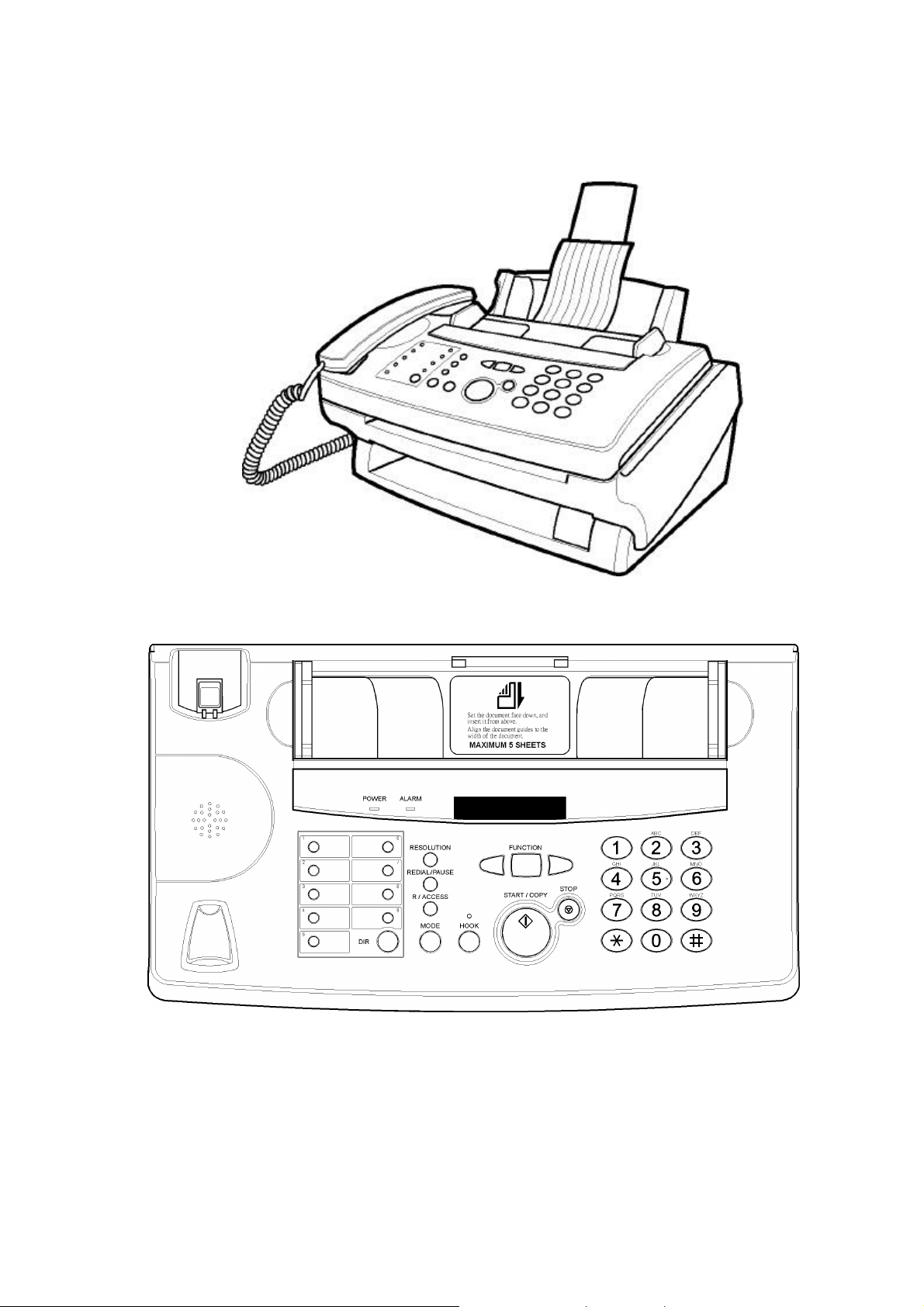
1.3 General Appearance
1.3.1 Appearance
1.3.2 Show the operation panel
1-7
Page 13

1.4 General Maintenance Function
- Self-diagnosis
(1) ROM VERSION
(2) PRINT TEST
(3) CHKSUM DISPLY
(4) LED TEST
(5) KEY TEST
(6) LCD TEST
(7) SENSOR TEST
(8) CCD Calibration
1-8
Page 14
2. INSTALLATIONS
2.1 General
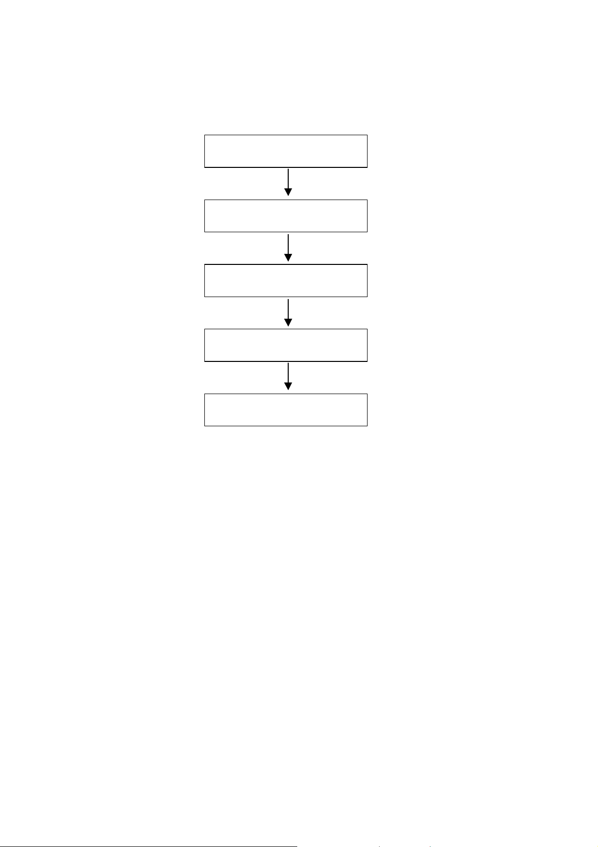
The following flowchart outlines the installation procedure.
Site selection (see 2.2)
Unpacking (see 2.3)
Check of contents (see 2.4)
Installation of attachments (see 2.5)
Initial setting
1-1
Page 15
2.2 Site Selection
The installation site
l Shall be free from outside vibrations, dust, etc.
l Shall not be directly exposed to sunlight and sudden changes in temperature.
l Must be horizontal and flat.
l Should have enough space in front of FAX machine to allow recording paper and
documents to be stacked;
l Shall not have any large, electrical noise-producing machine nearby.
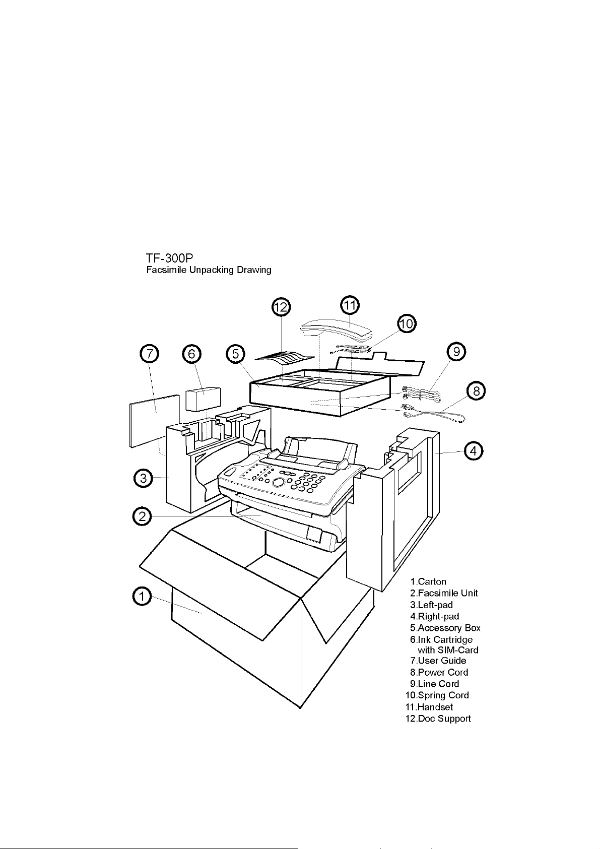
2.3 Unpacking
(1) Open the top cover of the cardboard box.
(2) Take out the machine with Styrofoam from the box.
(3) Take out the machine with plastic wrapper from the box.
1-2
Page 16
2.4 Check of Contents
After having taken out the machine and accompanied accessories from the cardboard box,
check the contents according to the following list:
(1) FAX machine
(2) Handset and Spring cord
(3) Documents Support
(4) AC cord
(5) Line cord
(6) User manual
(7) Ink Cartridge and SIM Card
2.5 Installation of Attachments
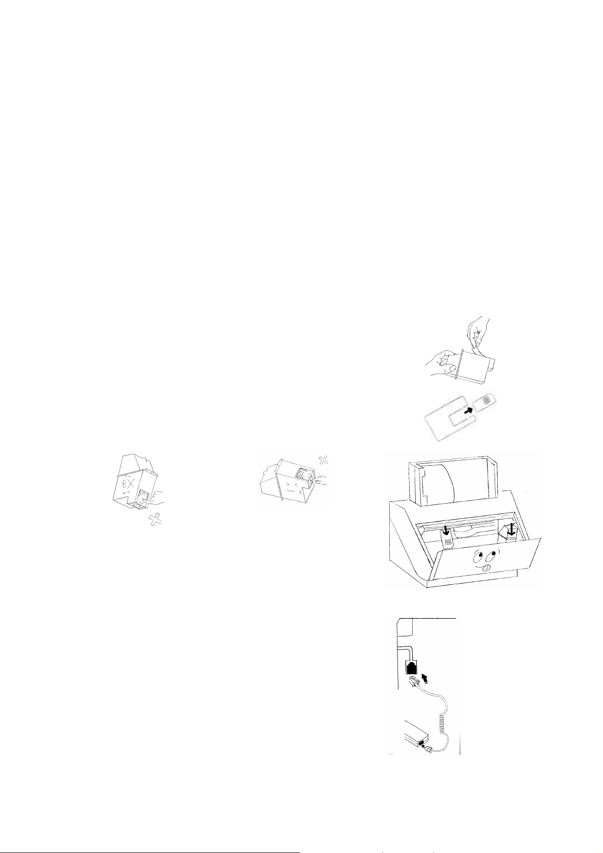
2.5.1 Cartridge and SIM Card
(1) Open the front cover.
(2) Remove the sealing tape from the printer head.
(3) Slide the cartridge in place.
(4) Push the lever up to lock the cartridge in position.
(5) Insert the new SIM card.
(6) Close the front cover properly using both hands.
¡¯ Avoid touching the nozzles and the electrical
contacts.
2.5.2 Handset and Line Cord
(1) Insert the handset cord into the socket upon the handset
and the other end into the socket on the base of the
facsimile.
(2) Plug the telephone line cord into the main unit.
(3) Connect the telephone or answering machine set to TEL
jack.
(4) Place handset on top of facsimile and slide the document
support into the holes on the cover of the facsimile.
(5) Plug in power cord and use the supplied cable to connect
the facsimile. (See 2.5.3)
1-3
Page 17
J After power on, the LCD will display the INITIALIZING for a period of time. This time
is used to clean the cartridge and warm up the printer.Insert the paper tray by holding it in an
upright position,
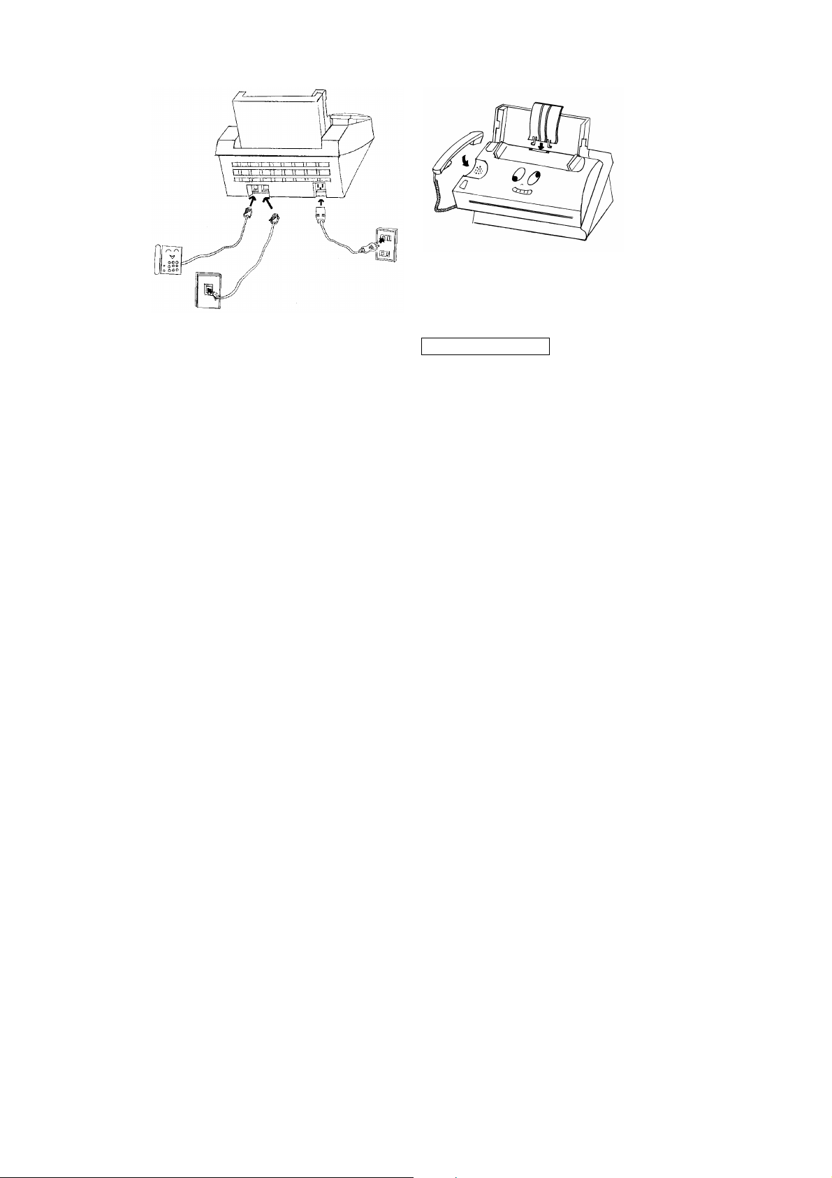
2.5.3 AC Cord Connection
(1) The power supply is provided as follows:
Voltage range 220~240 VAC, 50/60 HZ ± 3 Hz (EUROPE, AUSTRALIA)
or 100~120 VAC,50/60 Hz
(2) Check whether the voltage range of your input is within the above-mentioned voltage range
and if so, insert the mains lead into the power inlet on the back panel of the machine.
(3) Plug the main lead into a single wall outlet with a correct power supply, which is near to the
unit and is easily accessible.
(4) Check the display shows “(Date & Time)” standby mode.
1-4
Page 18
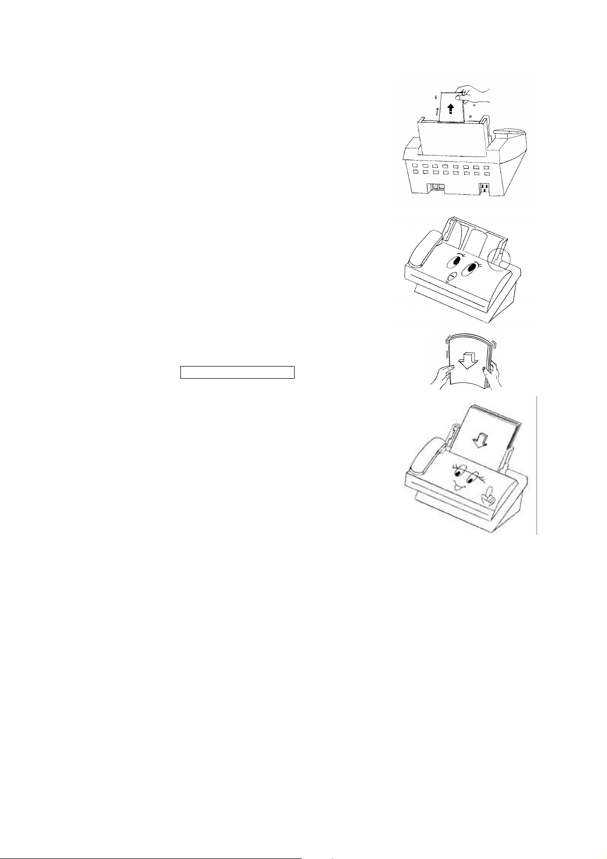
2.5.4 Loading Paper
(1) Pull out the paper support.
(2) Push the lever on the right side of paper cassette
backward.
Place the paper in the cassette so that the side you want
to print on faces you and the top of the page points
downward. Take care to keep the height of the stack below
the mark on the right side of the paper cassette.
(3) The cassette holds up to 50 sheets.
(4) Align the paper on the right side of the cassette and push it
down to the bottom.
(5) Adjust the left paper guide.
(6) Pull the lever toward the front of the machine. The paper is
held in place.
¡¯ If the machine runs out of paper during a print job, the
LCD shows ADD PAPER .
The fax will be stored in the memory and printed when
more papers are refilled.
1-5
Page 19

3. MAINTENANCE
3.1 Routine Inspection
Basically, the routine inspection of following items are performed about every one year after the
machine is installed. The description of routine inspection is shown in table 4.1.1.
Table 3-1 Routine Inspection
NO Inspection Item Procedure Remarks
1 I.S Platen Clean with ethyl alcohol.
2 A.D.F. roller Clean with ethyl alcohol.
Pick up roller Check the pick up rollers for wear.
Exit roller Clean with ethyl alcohol.
3 A.D.F. separation
rubber pad
4 Carrier Transport Check the following parts for wear:
5 Print head carrier
assembly
6 Contact Image Sensor
(C.I.S.)
7 Microswitch operation
Clean with warm or cold water.
If this rubber is worn out, replace this rubber.
·Carrier transport belt.
·Carrier guide rod.
·Idler pulley parts
Check it for a loose or worn wiper and cap.
Clean the contact of print head cable by a clean dry
cloth.
Check the following parts for wear or damage:
·Rubber Backer
·Print Cartridge Latch
·Latch Spring
·Carrier
Check it for stains of paper dust, etc.
Clean it with ethyl alcohol, if necessary.
Cover switch Confirm that the LCD shows “CLOSE COVER”.
When the paper cover opened and that message
disappears when the cover closed.
·Paper sensor
8 Lubrication Apply white grease to the motor gear and all gear
9 Cleaning Remove outside fallen materials, if any, from the
Note:
When returning all rollers to its original position, confirm that its plastic bushing of the roller
properly set into the groove of the frame unit and turn the bushing to make sure the pin point of
tab is tightly inserted to the frame surface.
The LCD shows “ADD PAPER” when runs out of
recording paper.
mounting stud when parts are replaced or as needed.
The carrier to carrier frame engagement.
machine.
3-1
Page 20
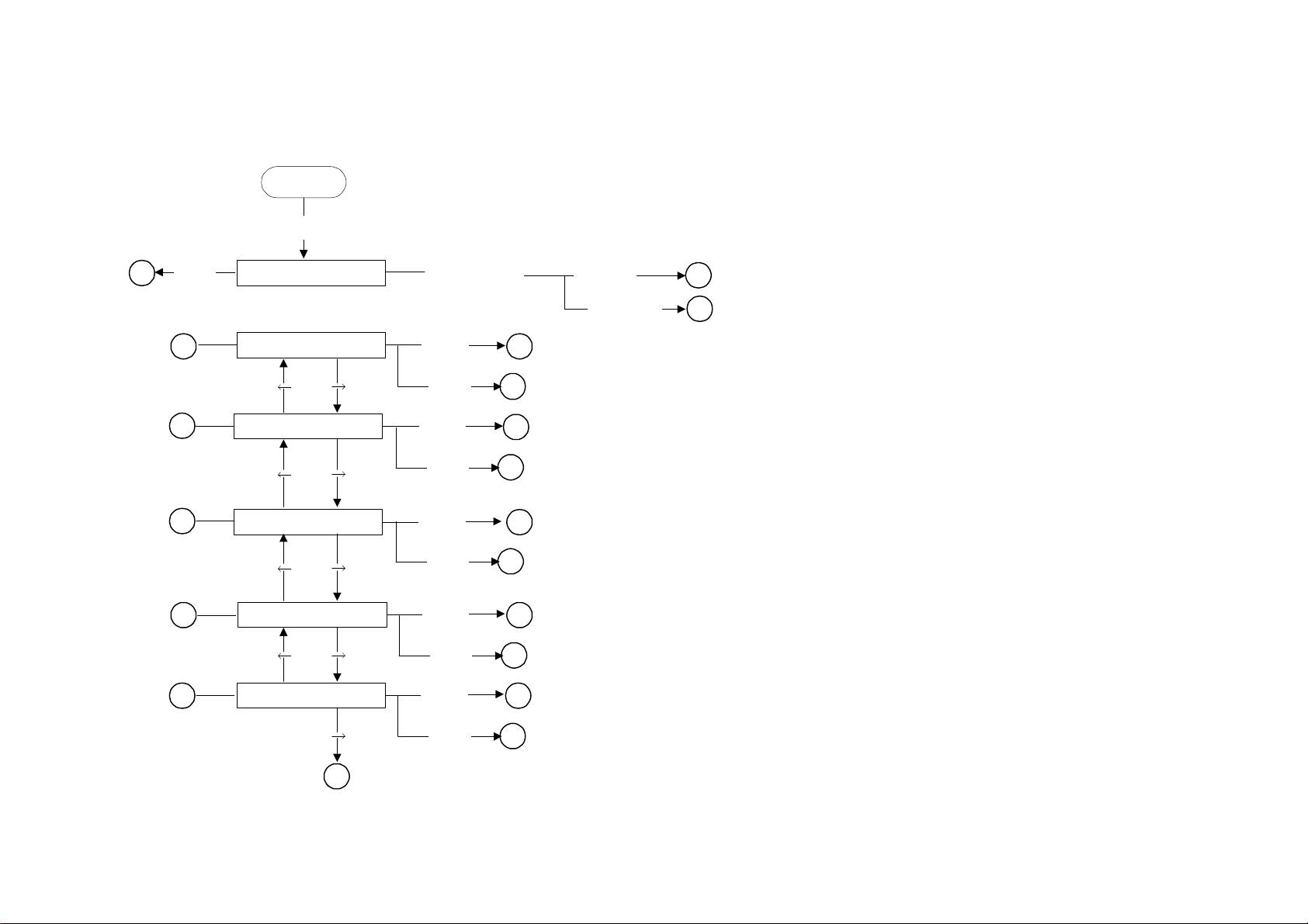
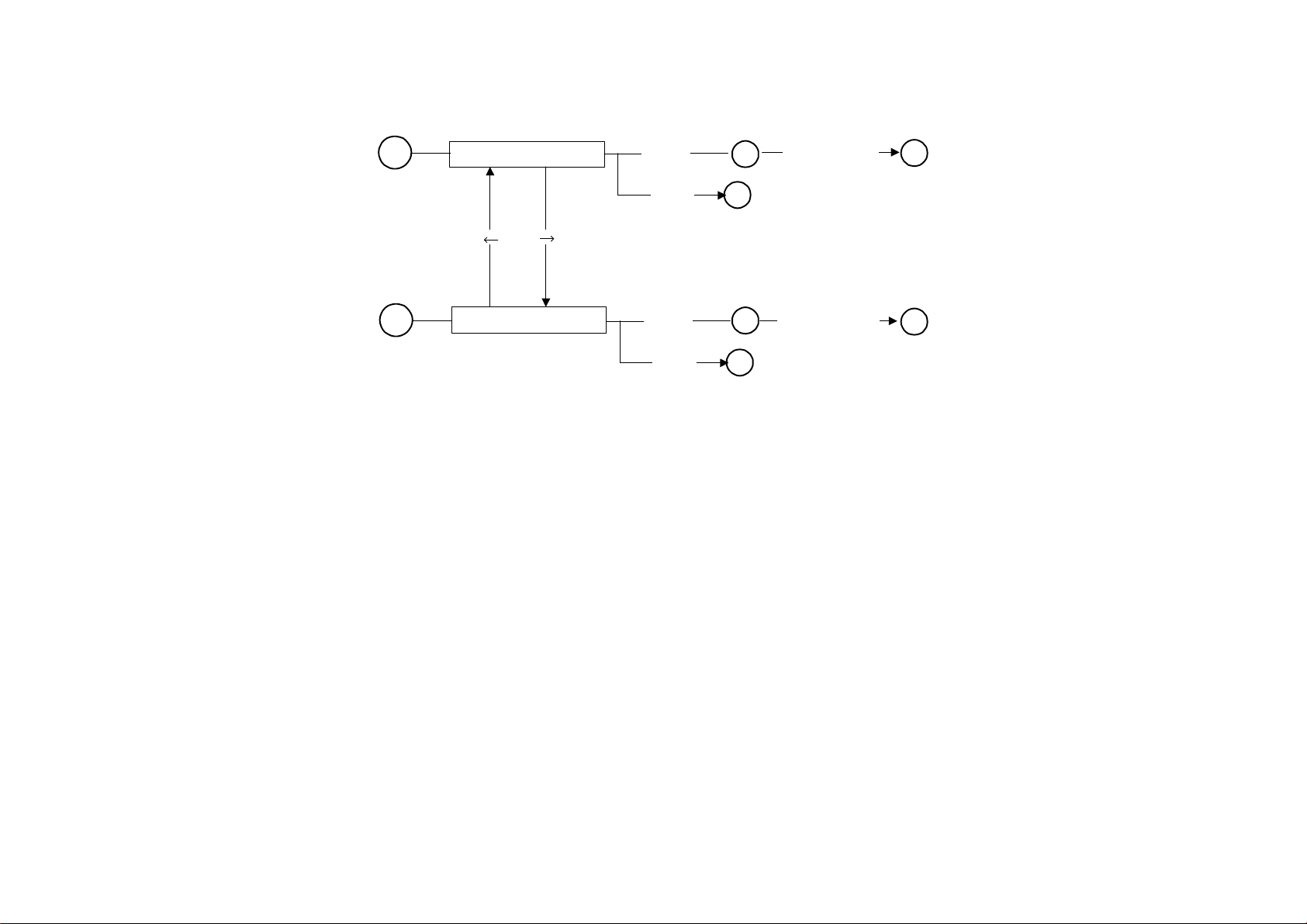
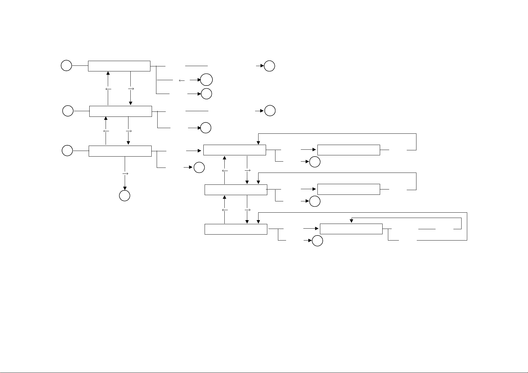
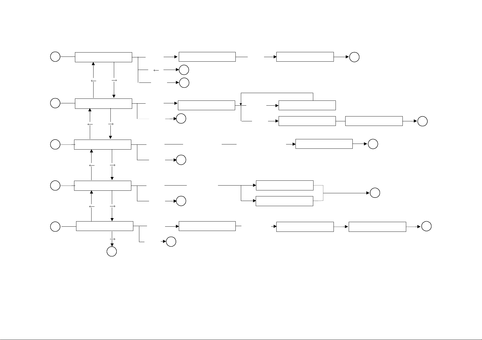
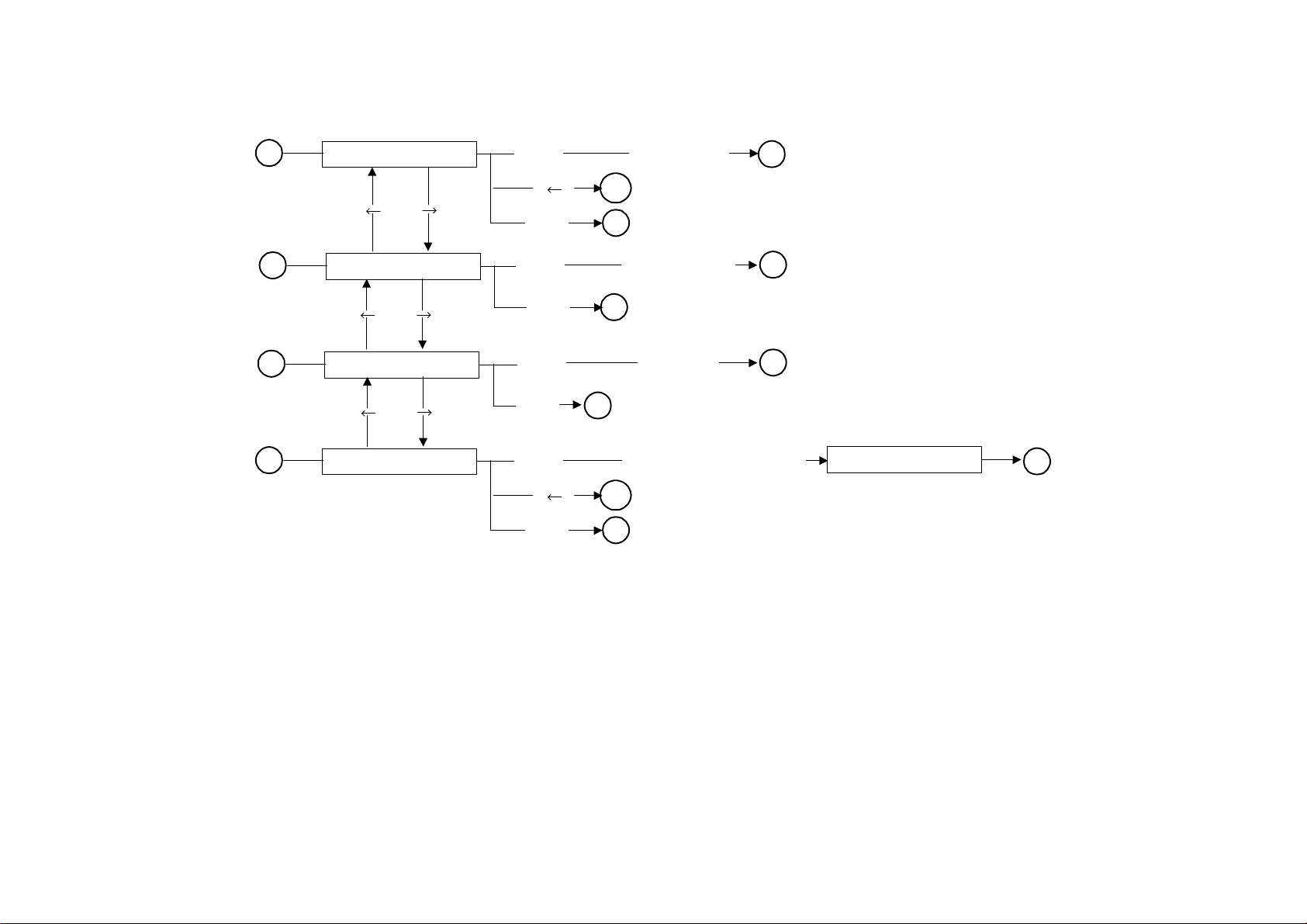
4. SYSTEM TEST
POWER ON
TURN ON THE POWER
AND PRESS FUNCTION
KEY AT THE SAME TIME
<[FUNCTION]>
PRESS AND HOLD 2 SEC
<[STOP]>
A
8.1
8.2
8.3
8.4
SYSTEM TEST
SERVICE SET
<[
<[ ]>
SERVICE LIST
<[ ]>
<[ ]>
SERVICE TEST
<[ ]>
<[ ]>
SERVICE CLEAR
PRESS 54188
<[START]>
]>
<[STOP]>
<[START]>
<[STOP]>
<[START]>
<[STOP]>
<[START]>
8.1.1
A
8.2.1
A
8.3.1
A
8.4.1
CODE ERROR
CODE CORRECT
A
8.1
<[STOP]>
<[START]>
<[STOP]>
AGAIN?
<[ ]>
<[
8.1
]>
<[ ]>
8.5
A
8.1
A
4-1
Page 21
8.1.1
CLOCK FORMAT
<[ ]>
<[ ]>
<[START]>
<[ ]>
<[STOP]>
=D/M/12H [ ]
8.1.11
8.1
<[ ] [ ]>
<[START]> UPADATE
<[STOP]>
60
CHANGE DISPLAY (M/D/12H)/ (D/M/24H)/ (M/D/24H)
8.1.1
A
8.1.2
8.1.2
8.1.3
8.1.4
XMT MODEM SPEED
<[ ]>
<[ ]>
RCV MODEM SPEED
<[ ]>
<[ ]>
MODEM XMT LEVEL
<[ ]>
8.1.5
<[START]>
<[STOP]>
<[START]>
<[STOP]>
<[START]>
<[STOP]> 8.1
=9600 [ ]
8.1
=9600 [ ]
8.1
=-10 [ ]
<[ ] [ ]>
<[START]>
<[STOP]>
60
A
<[ ] [ ]>
<[START]>
<[STOP]>
60
A
<[ ] [ ]>
<[START]>
<[STOP]>
60
A
CHANGE SPEED (7200) / (4800)/(2400)
UPADATE
8.1.2
8.1.3
CHANGE SPEED (7200) / (4800)/(2400)
UPADATE
8.1.3
8.1.4
CHANGE DISPLAY ( 0 ~ -15 )
UPADATE
8.1.4
8.1.5
4-2
Page 22

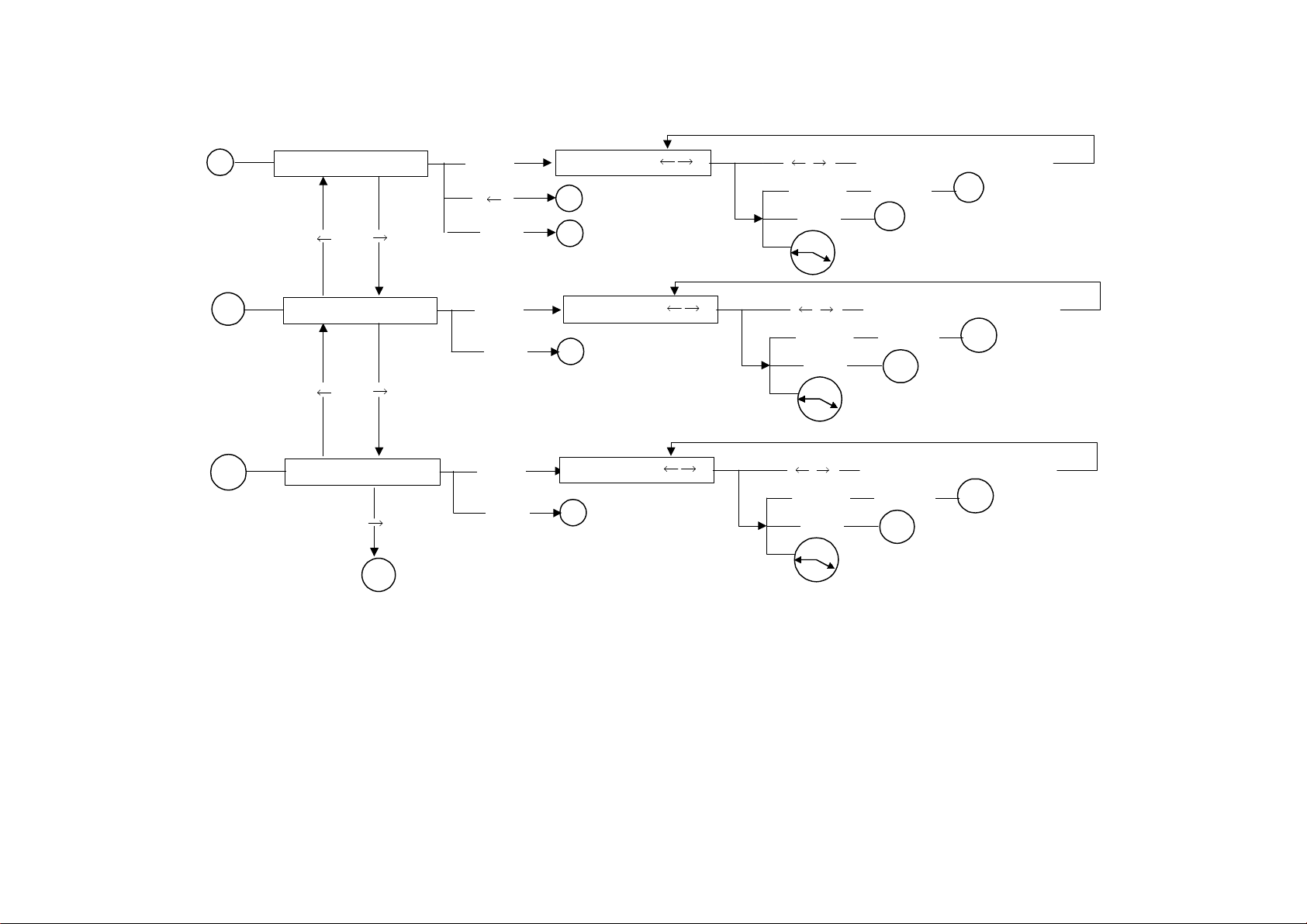
8.1.5
DIAL TONE CHECK
<[ ]>
<[ ]>
<[START]>
<[ ]>
<[STOP]>
=ON PBX/ON PSTN
8.1.4
8.1
<[ ] [ ]>
<[START]> UPADATE
<[STOP]>
60
A
CHANGE COMBINATION
8.1.5
8.1.6
8.1.6
8.1.7
8.1.8
BUSY TONE CHECK
<[ ]>
<[ ]>
CNG DETECT
<[ ]>
<[ ]>
CNG XMT DELAY
<[ ]>
8.1.9
<[START]>
<[STOP]>
<[START]>
<[STOP]>
<[START]>
<[STOP]> 8.1
=ON PBX/ON PSTN
8.1
=ON [ ]
8.1
=ON [ ]
<[ ] [ ]>
<[START]>
<[STOP]>
60
A
<[ ] [ ]>
<[START]>
<[STOP]>
60
A
<[ ] [ ]>
<[START]>
<[STOP]>
60
A
CHANGE COMBINATION
UPADATE
8.1.6
8.1.7
CHANGE DISPLAY (ON) / (OFF)
UPADATE
8.1.7
8.1.8
CHANGE DISPLAY (ON) / (OFF)
UPADATE
8.1.8
8.1.9
4-3
Page 23
8.1.9
INT'L DIAL TONE
<[
<[
]>
]>
<[START]>
<[
<[STOP]>
=ON [ ]
]>
8.1.8
8.1
<[ ] [ ]>
<[START]>
<[STOP]>
60
A
CHANGE DISPLAY (ON) / (OFF)
UPADATE
8.1.9
8.1.10
8.1.10
8.1.11
T.30 MONITOR
<[
<[
]>
AUTO REDIAL
<[
8.1.1
<[START]>
<[STOP]>
]>
<[START]>
]>
<[STOP]>
=ON [ ]
8.1
=1 [ ]
8.1
<[ ] [ ]>
<[START]>
<[STOP]>
60
A
<[ ] [ ]>
<[START]>
<[STOP]>
60
A
CHANGE DISPLAY (ON) / (OFF)
UPADATE
8.1.10
8.1.11
CHANGE DISPLAY 1~9
UPADATE
8.1.11
8.1.1
4-4
Page 24
8.2.1
PRT SERVICE LIST
<[START]>
71
PRINT SERVICE LIST
8.2.2
<[STOP]>
<[ ]>
8.2.2 71
PRT TEST PATTERN
<[ ]>
<[START]>
<[STOP]>
8.2
8.2
PRINT TEST PATTERN
8.2.1
4-5
Page 25
8.3.1
SCANNER TEST
<[
<[
]>
<[START]>
<[
]>
]>
<[STOP]>
ROATE SCANNER MOTOR
5SEC THEN STOP
8.3.8
8.3
8.3.2
8.3.2
8.3.3
PRINTER TEST
<[
<[
]>
MODEM TEST
<[
8.3.4
<[START]>
]>
]>
<[STOP]>
<[START]>
<[STOP]>
ROATE PRINTER MOTOR
5SEC THEN STOP
8.3
TX TONE 1100 HZ
8.3
<[
<[
]>
TX TONE 2100HZ
<[
<[
]>
TX DTMF
8.3.3
<[START]>
<[STOP]>
]>
<[START]>
<[STOP]>
]>
<[START]>
<[STOP]>
XMTTING 1100HZ
8.3.3
XMTTING 2100HZ
8.3.3
TX DTMF=_
8.3.3
<[STOP]>
<[STOP]>
<[0~9, ¡¯, # ]>
<[STOP]>
CHANGE
DISPLAY
4-6
Page 26
8.3.4
SENSOR TEST
<[
<[
]>
<[START]>
<[
]>
]>
<[STOP]>
P, D1, D2, C =XXXX
P=PAPER SENSOR
8.3.3
D1=DOC SENSOR 1
D2=DOC SENSOR 2
C=COVER SENSOR
8.3
X=0 OR 1
<[STOP]>
SENSOR TEST END
8.3.5
8.3.5
8.3.6 <[START]>
8.3.7 <[START]>
8.3.8
KEY TEST
<[
<[
]>
]>
LED/LCD TEST
<[
<[
]>
]>
DRAM TEST
<[
<[
]>
]>
CIS CALIBRATION
<[
]>
8.3.1
<[START]>
<[STOP]>
<[STOP]>
<[STOP]>
<[START]>
<[STOP]> 8.3
PLEASE ENTER KEY
8.3
TURN ON ALL LEDS
5SEC THEN TURN OFF
8.3
WRITE DRAM AND
READ DRAM
8.3
PUT WHITE PAPER
ANY KEY IN
<[STOP]>
DISPLAY ASCII CHARACTERS
CONTUNUOUSLY
OK
NG
<INSERT PAPER>
DRAM TEST OK
DRAM TEST NG
X PRESSED
STOP PRESSED KEY TEST END
LED/LCD TEST END
8.3.7
8.3.8
DOCUMENT IN CIS CALIBRATED
8.3.6
8.3.1
4-7
Page 27
8.4.1
USER OPTION
<[START]>
RESET USER OPTION
TO DEFAULT VALUE
8.4.2
8.4.2
8.4.3
8.4.4
<[ ]>
<[ ]>
SERVICE OPTION
<[ ]>
<[ ]>
DRAM
<[ ]>
<[ ]>
ALL RAM
<[ ]>
<[STOP]>
<[START]>
<[STOP]>
<[START]>
<[STOP]>
<[START]>
<[ ]>
<[STOP]>
8.4.4
8.4
RESET SERVICE OPTION
TO DEFAULT VALUE
8.4
INITIALEZE DRAM
8.4
RESET USER OPTION, SERVICE OPTION
TO DEFAULT VALUE & INITIALIZE DRAM
8.4.1
8.4
8.4.3
8.4.4
MEMORY CLEAR
8.4.1
4-8
Page 28

5. MECHANICAL DISASSEMBLY AND REASSEMBLY
This chapter explains the procedures for replacement of parts, assembles and units in the field.
5.1 General
5.1.1 PRECAUTIONS PARTS REPLACEMENT
(1) Before starting disassembly and re-assembly, always turn the AC power switch OFF, and pull
out the AC plug.
(2) Since screws, small parts are likely to be lost, they should temporarily be attached to their
original positions.
(3) When handing items such as circuit boards, do not wear gloves that are likely to generate
static electricity.
(4) Do not place printed circuit boards directly on the equipment or on the floor.
5.1.2 TOOLS
The table shows the tools required for replacement of parts such as circuit boards and
mechanical units.
ITEM SERVICE TOOLS TYPE Q’TY REMARKS
1 PHILIPS SCREWDRIVER (L) RUBICON 107 1 M3 SCREW
2 PHILIPS SCREWDRIVER (M) RUBICON 102 1 M2.6 SCREW
3 PHILIPS SCREWDRIVER (S) RUBICON 104 1 M2.3 SCREW
4 STRAIGHT SCREWDRIVER RUBICON 101 1 E RING
5 RADIO PLIERS 1
6 CUTTING PLIERS 4” 1
7 MULTIMETER 1 SHORT-
CIRCUIT TEST
8 DIGITAL STORAGE
OSCILLOSCOPE 100MHZ(UP)
9 OFFSET TYPE SCREWDRIVER NO.2 1
1
5-1
Page 29
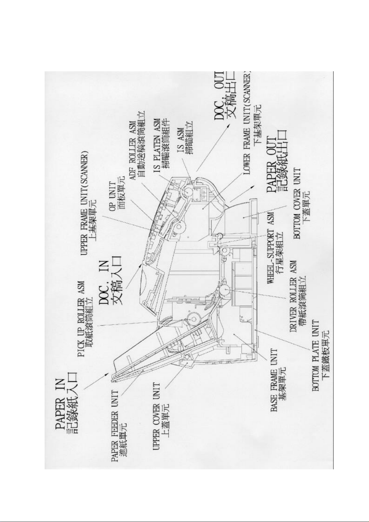
5.2 General Mechanical Structure
The general mechanical structure of the FAX machine is shown:
5-2
Page 30
5.3 How to Disassemble and Reassemble
This item explains how to dismantle and assemble this FAX machine. Figure 5-3 Scanner
Mode Unit and Figure 5-7 Printer Mode Unitshow the procedure flow of dismantlement in brief.
The detailed procedure of dismantlement is explained from sub-item 5.3.1 to 5.3.17
The steps of dismantlement, reversing the steps of assembly, are shown as follows. For the
convenience of explanation, some definitions are stated as follows:
1) The Front of machine means the face of operation panel.
2) The Left and Right mean the left and right hand side facing from the front of machine.
3) The directions of Clockwise and Counterclockwise are defined viewing from the right of
machine.
5.3.1 Installing the Ink Cartridge and SIM Card
You can buy replacement mono cartridges from all OKI shops, main electrical retailers and good
stationers.
Black (item code)
1) After lifting the handset , please open the operational panel directly.
2) To install a new Ink Cartridge. Remove the sealing tape from the printed head.
3) Slide the Ink Cartridge into carriage then push it down.
4) Insert new SIM Card
5) Close the Operational Panel.
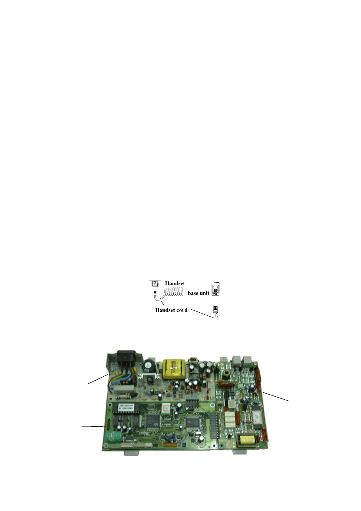
5.3.2 AC plug, Handset and Doc. Support
1) Face the rear of machine, pull out the AC plug, handset cord and line cord .
2) Take off the power cord, handset and Doc. Support.
Figure 5-1
5.3.3 Bottom Plate Unit
Power
Board
NCU
Board
Main
Board
Figure 5-2 Bottom Plate Unit
5-3
Page 31

¡° Note:
Put a softer plate on table to avoid operation panel to be scratched is necessary.
1) Face the bottom of machine, loosen 2 pieces of M3X8 tapping screws then open Bottom Plate
Asm. from Bottom Cover.
2) Bottom Plate Asm.
Pull out all connectors on Main Board, NCU Board and Power Board , then Bottom Plate Asm.
can be taken out from Bottom Cover.
3) NCU Board Asm. , Main Board Asm. , Power Board Asm.
Loosen 3 pieces of M3X6 taptite screw for NCU Board, 2 pieces for Main Board and 2 pieces
for Power Board then NCU Board Asm, Main Board Asm. and Power Board Asm. can be
taken out from Bottom Plate.
4) Insulation
Take out Insulation sheet from Bottom Plate.
5) Separate Rubber Leg and Insulation Sheet.
5.3.4 SIM Card Holder Assembly
(1) Face the bottom of machine, loosen 1 piece of M3X12 tapping cap screw.
(2) SIM Card Holder Asm
Open Operational Panel, loosen 1 piece of M3X12 tapping cap screw for SIM Card Holder
and SIM Card Cover then SIM Card Holder Asm can be take out from machine.
(3) SIM Card Holder, SIM Card Cover and SIM Card PCB Asm.
Loosen 1 piece of M3X8 tapping cap screw for fixing Sim Card Holder and SIM Card Cover
then can separate SIM Card Holder, SIM Card Cover and SIM Card PCB AIM.
5.3.5 Scanner Mode Unit
Upper Cover Unit
Lower Frame Unit
Upper Frame Unit
Figure 5-3 Scanner Mode Unit
(1) Open Operational Panel and rotate Pull Tie that fixed on OP Bracket until one side of Pull Tie
can be taken out from OP Bracket. Loosen 1 piece ofM3X8 tapping screw that fix another
side of Pull Tie on Upper Cover then it can be taken out from Scanner Mode Unit.
(2) Loosen 1 piece of M3X8 tapping screw that fix on right side of Upper Cover and release the 4
latches that fix Upper Cover and Bottom Cover. Lift Scanner Mode Unit and all cables can be
5-4
Page 32

pulled out from Printer Mode Unit then both units can be separated.
(3) Loosen 3 pieces of M3X8 tapping screws that fix Lower Frame and Upper Cover Unit then
Scanner Mode Asm. and Upper Cover Unit can be separated.
5.3.6 Scanner Mode Asm.
Figure 5-4 Scanner Mode Asm.
Scanner Unit
OP Unit
Loosen 4 pieces of M3X8 tapping screws that fix Scanner Unit and O/P Unit. Cut the Cable Tie
that fasten Ground Wire and Cable Tube on left hand side. Pull out two connectors of ADF
sensor and DOC Sensor then Scanner Unit and O/P Unit can be separated.
5.3.7 Scanner Unit
Lower Frame
Upper Frame
Rotate 90°of clockwise for Upper Frame Unit then Lower Frame Unit and Upper Frame Unit can
be separated.
5.3.8 Lower Frame Unit
(1) Loosen 1 piece of M3X6 tapping screw on right side of I.S. Platen then move Ground
Spring.
(2) Loosen 1 piece of M3X6 tapping screw on right side of A.D.F. Roller then move Ground
Spring . Take out Ground wire from indent of Lower Frame.
Figure 5-5 Scanner Unit
5-5
Page 33

(3) Loosen 1 piece of M2.6X5 tapping screw on right side for fix Cover Switch Sensor then
move Cover Switch Sensor.
(4) I.S. Platen Asesmbly
¬ Face white I.S. Platen Asm., Gear is located on left side. With a straight screwdriver, pull
upward the snap of bushings( green )at the left and right ends of I.S. Platen , and grip
bushings with both hands and rotate it upward to vertical direction then take I.S. Platen
Asm. out.
- Use finger to release the Snap of Gear then Gear can be separated from the shaft of I.S.
Platen.
® Use small straight screwdriver to pick E-Ring on both side of I.S. Platen then take out left
and right bushing.
(5) Loosen 1 piece of M2.6X5 tapping cap screw on spindle of gear than take out 1 piece of
70/20 gear and 2 pieces of 36/20 gear.
(6) I.S. Asesmbly
¬ Compress both hinges of the I.S. assembly a bit and push the I.S. assembly from left to
right until the left hinge can be separated with its spindle on the scanner frame, remove
the I.S. assembly from left slantwise.
- Separated I.S. Cable from Tie Mount and pull out the connector of the I.S. cable.
® Release 4 pieces of M2.6X6 tapping screw on both side of I.S. Asm. then these two
Hinges can be separated from I.S.
(7) Loosen 2 pieces of M3X6 taptite screw for fixing I.S. Motor. Separate the cable of Motor
then I.S. Motor can be taken out from Lower Frame.
(8) With a straight screwdriver , pull upward the snap of bushings( black) at the left and right
ends of the A.D.F shaft, and grip bushings with both hands to take A.D.F. assembly out.
(9) Remove a black bushing on one side of the A.D.F assembly. Release the “E” ring on the
outside of gear by straight screwdriver, takes out clutch gear, clutch spring, clutch bushing
and another black bushing.
(10) With a straight screwdriver, press the both side of Flat Spring-IS then Flat Springs can be
picked out of Lower Frame.
(11) Separate Snap Rivet and flat Spring.
5.3.9 Upper Frame Unit.
(1) Ground Wire
Loosen 1 piece of M3X6 tapping screw. Pull out the ground wire pin of Separation Asm then
ground wire can be taken out.
(2) Spring Hook
Loosen both side of M3X6 tapping screws then both spring -hook can be taken out.
(3) A.D.F. sensor Asm.
Release snap-in fingers of ADF sensor assembly by a straight screwdriver then remove the
ADF sensor Asm.
(4) DOC. sensor Asm.
Release snap-in fingers of DOC. sensor assembly by a straight screwdriver then remove the
DOC. sensor Asm.
(5) Separation Asm.
¬ Take out A.D.F. Extension Spring from Upper Frame.
- With a straight screwdriver, take out Separation Asm.
(6) Push up clamping plate then separation plate and backing plate can be pulled out.CIRCUIT
DISCRIPTION
5-6
Page 34

5.3.10 Document Guide Assembly
(1) Use a straight screwdriver to separate Operational Panel and Doc. Guide Asm.
(2) Setting Spring & Spur Gear
Press downward the Setting Spring and move to longer side. Then Setting Spring and Spur
Gear can be taken out at the same time.
(3) DOC. Guide
¬ Lift slightly and pull the left Document Guide outward to take it out.
- Lift slightly and pull the right Document Guide outward to take it out.
(4) DOC. Setting Lable
DOC. Setting Lable can be scratched from DOC. Bracket.
5.3.11 Operation Panel Unit
Figure 5-6 Operation Panel Unit
(1) O/P Bracket & Hook Switch Assembly
With a cross screwdriver, loosen 5 pieces of M3X8 tapping screw for fixing O/P Bracket.
Then O/P Bracket can be taken out from O/P Asm. At the same time, pull out Hook Switch
Asm. from O/P Bracket.
¡°
Note:
Put a softer plate on table to avoid operation panel to be scratched is necessary.
(2) Pull out connectors on the key board and hook switch board . Take out cable from two
mounts.
(3) Buzzer
Loosen two pieces of M2X6 taptite screw for fixing buzzer then buzzer can be taken out.
(4) Key Board, Key Pad, Number Key, Function Key, Facility Key, Stop Key, Start/Copy Key
Use a small cross screwdriver to loosen 10 pieces of M2X6 taptite screw for fixing Key Board
then Key Board, Key Pad, Number Key, Function Key, Facility Key, Stop Key, Start/Copy
Key can be taken out respectively.
(5) Display Panel
Use a straight screwdriver to pick Display Panel from the gap between Display Panle and O/P
on right or left side.
(6) Use a straight screwdriver to peel Quickdial Card Cover from the gap on right side then pick
Quickdial Card.
5-7
Page 35

5.3.12 Upper Cover Unit
(1) Paper Sensor assembly and Bottom Cover
Release snap-in fingers of Paper Sensor Asm. by a straight screwdriver, then can separate
Paper Sensor Asm. and Bottom Cover.
5.3.13 Printer Mode Unit
Printer Mode
Asm.
Bottom Cover
Unit
(1) Printer Mode Asm. & Bottom Cover Unit
Loosen 4 pieces of M3X8 tapping screw then Printer Mode Asm. can be taken out form
Bottom Cover Unit.
5.3.14 Printer Mode Asm.
Figure 5-7 Printer Mode Unit
Figure 5-8 Printer Mode Asm.
(1) Ground Wire
Loosen 1 piece of M3X6 tatite screw for fixing ground wire by a cross screwdriver then
ground wire can be taken out from Printer Bar.
(2) Loosen 2 pieces of M3X10 tapping cap screw on right and left side of Paper Feeder Unit
5-8
Page 36

with a cross straight screwdriver.
(3) Loosen 2 pieces of M3X12 tapping cap screw(with a Spring Washer on right side screw) on
right and left side of Base Frame Unit with a cross straight screwdriver then Paper Feeder
Unit and Base Frame Unit can be separated.
5.3.15 Paper Feeder Unit
Figure 5-9 Paper Feeder Unit
(1) Ground Spring & Ground Wire
Loosen 1 piece of M3X6 tapping cap screw on Handle side by cross screwdriver then
Ground Spring and Ground Wire can be taken out from Paper Feeder Unit.
(2) Pick Up Roller Clutch & E-ring
Face the Gear-Pick Up side of Paper Feeder Unit. Release the E- ring (£X4 )on the outside
of gear by straight screwdriver then take out Pick Up Roller Clutch and E-ring.
(3) E-ring
Release the E- ring (£X4) on the both side of Paper Feeder Unit by straight screwdriver
then take out E-ring.
(4) Sintering Bearing
Move outward two Sintering Bearing then take them out.
(5) Pick Up Roller Asm.
Remove Pick Up Roller Asm. leftward then upward. Pick Up Roller Asm. can be taken out
from Paper Feeder Unit.
(6) Handle & Spring-Handle
Face the Handle side of the Paper Feeder Unit. Loosen 1 piece of M3X6 taptite cap screw
by cross screwdriver then it and Spring-Handle can be taken out.
(7) Spring-Buckle Corner
Take out Spring-Buckle Corner by hook.
(8) Buckle Corner
Face the Plane-Knock Up. Pull Buckle Corner up and outward then it can be taken out.
(9) Plate –Knock Up
Hold left side of Frame-AFP by left hand. Wrench left side of Plate-Knock up by thumb of
right hand then fixed position pin of Plate-Knock Up will be taken out. Face the rear of
Frame-APF, release the snap of Plate-Knock Up from Linkage then Plate-Knock Up can be
taken out from Frame-APF.
(10) Paper Support
5-9
Page 37

Pull Paper Support to highest point. Widen the gap that between Frame and Paper Support
by straight screwdriver then Paper Support can be drawn out from Frame.
(11) Spring-Knock Up
Pull out two Springs-Knock Up from Frame-APF.
(12) Linkage
Face the rear of Frame-AFP, pull linkage out from snap of Frame.
(13) Paper Guide-APF
Face the bear of Plate, pull out the elastic snap by straight screwdriver then Paper Guide
can be taken out from Plate.
(14) Cork Plate
Pull out Cork Plates from Plate.
5.3.16 Base Frame Unit
Figure 5-10 Base Frame Unit
(1) Idle roller
Release 2 pieces of M3X 6 taptite screws from Printer Control Board for fixing Paper guide
Asm. then it can be taken out from Printer Bar. Take 4 Idle Roller out from Baseframe.
(2) Paperguide Asm.
¬ Snap out 4 pieces of Spring from Paperguide Frame by Spring-Hook.
- Paperguide Pin, Paperguide Frame, Paperguide
Draw out Paperguide Pin from Paperguide then Paperguide Frame and Paperguide can
be separated.
® Spring-Paperguide
Take out 4 pieces of Spring-Paperguide from Paperguide.
(3) APF Sensor Asm.
Pull out all connectors on Printer Control Board. Release snap-in fingers of APF sensor
assembly by a straight screwdriver, remove the AFP sensor assembly.
(4) Paper Motor:
5-10
Page 38

¬ Cut Cable Tie for Fixing Cable Asm.
- Loosen 2 pieces of M3×6 taptite screws, remove the motor.
(5) Gear A, Gear B, Gear C
Release 2 pieces of M2X6 tapping screw then Gear B(2X), GEAR A and Gear C can be
taken out in sequence.
(6) Gear D, Driver Roller Gear
Release the snap of Gear D for fixing on Baseframe then Gear D and 2 pieces of Driver
Roller Gear can be taken out from Baseframe.
(7) Print Bar
Release 2 pieces of M3X8 tapping screw for fixing Printer Bar. Remove Print Bar Upward
and Forward then it can be taken out from Bracket-BF-L&R.
(8) Printer Control Board
¬ Drop Detect Cable
Pull out both connectors that connect Service Station and Printer Control Board then Drop
Detect Cable can be taken out.
- Release Flex Cable connector then Carriage Flex Cable can be taken out from Printer
Control Board.
® Release 2 pieces of M3X6 taptite screw for fixing Printer Control Board then it can be
taken out from Print Bar.
(9) Bracket-Bf-R
Release 2 pieces of M3X6 tapping Screw for fixing Bracket-bf-R on Base Frame then it can
be taken out.
(10) Bracket-Bf-L
Release 4 pieces of M3X6 tapping Screw for fixing Bracket-bf-L on Base Frame then it can
be taken out.
(11) Ground Spring & Ground Wire
Release 2 pieces of M3X6 tapping screw for fixing Ground Spring(2X) and Ground Wire
then they can be taken out.
(12) Driver Roller
Face the bottom of Base Frame. With a straight screwdriver, pull upward the snap bushings
at the left and right ends of Driver Roller and grip bushings with both hands to take it out.
(13) Exit Roller
Face the bottom of Base Frame. With a straight screwdriver, pull upward the snap bushings
at the left and right ends of Exit Roller and grip bushings with both hands to take it out.
(14) Wheel Support Asm.
¬ Release 1 piece of M3X6 tapping Screw. Lift left side of Wheel Support then it can be
taken out from fixed position on Base Frame.
- Star Wheel, Star Wheel Spring & Wheel Support
Take out 6 pieces of Star Wheel Spring and Star Wheel from Wheel Support.
5.3.17 Bottom Cover Unit
(1) Speaker Asm.
Release the snap for fixing Speaker Asm. then it can be taken out from Bottom Cover.
(2) EVA-Speaker 1 & EVA-Speaker 2
Pull EVA-Speaker 1 and EVA-Speaker 2 from speaker.
5-11
Page 39

(3) Socket-616E Cable Asm.
Release 2 snap for fixing Socket-616E Cable Asm. then it can be taken out from Bottom
Cover.
(4) Rubber Leg
Face the bottom of Bottom Cover. Take out 4 pieces of Rubber Leg.
5-12
Page 40

6. CIRCUIT DESCRIPTION
6.1 Main Board Circuit
The mother board version is the first version that begins mass-production and the circuit diagrams
consists of 11 schematics which are described in the following sections.
6.1.1 Block Diagram
The extended FAXENGINE chip set consists of an Integrated Fax Controller FC200(-M) and a
modem chip (R96DFXL). The FC200(-M) performs all common facsimile machine control, monitor
and interface function. Additionally, it contains scanner, printer, keyboard, stepping motor and
modem interfaces. These programmable functions and interfaces support a wide range of
peripherals. Integrated 8 bit pipeline ADC, clamp, sample hold and AGC allow minimum external
scanner interface hardware. Built-in DLC and shading correction combined with two-dimensional
Error Diffusion and two-dimensional edge enhancement provides state-of-the-art image processing
performance in half-tone modes. The R96DFXL modem can execute modem can excu 9600bps
fax transmission and reception.
6.1.2 Integrated Fax Controller
The Advanced extended FAXENGINE Integrated Fax Controller (FC200-M) includes following
features.
1) Microprocessor.
The embedded processor MC24TM in FC200(-M) provides 16-Mbyte memory addressing
capability over 24-bit address/8-bit data bus and dedicated control lines.
2) Printer Interface Control.
The FC200(-M) supplies programmable strobe and control signals that interface with most, if not
all, thermal printers. In addition to Standard (non-Split) printing mode, latchless Split-printing
mode and latchless two-clock mode can be supported. The three signals PDAT, PCLK, and PLAT
control the transfer of data to the printer.
3) Scanner Control.
Four programmable control and timing signals supports CIS scanner interface. An internal 8-bit
A/D converter is provided. Video processing supports DLC and two modes of shading correction
for scanner data non-uniformity’ s arising from uneven sensor output or uneven illumination.
Correction may be provided to an 8-pixel group at a time or, separately to each pixel. Less than 1
K of RAM is required to support shading correction. A Digital Adaptive Halftone image processing
is supported. A 2-Dimensional error diffusion algorithm as well as a 2-D Edge Enhancement
control are performed in the hardware. Dynamic background and contrast control is provided for
text images. Multi-level horizontal B4 to A4 reduction is also provided for the scanner data.
4) Motor Control.
Eight outputs are provided to external current drivers; four for scanner motor.
5) Image Coding Schemes.
FC200 (-M) provides MMR data compression and decompression conformed with ITU-T
recommendation T.4.
6) Real Time Clock (RTC).
FC200 (-M) includes a battery backed-up real time clock. The life of the RTC is 32 years, and leap
year compensation is automatic.
7) External Memory Support.
External ROM stores the program object code. External RAM is used by processor for shading
correction and line buffer. DRAM controller supports refresh during battery operation. DRAM
stores image and voice data.
6-1
Page 41

8) Modem Interface.
FC200 (-M) runs at a clock derived from modem clock. FC200 (-M) immediately handles interrupt
request from modem in order to keep constant transmission flow.
9) Panel Interface.
Four inputs, eight strobe outputs, and two control outputs support keys scan and LCD driver.
10) Battery and Power.
FC200 (-M) detects power failure and switches to battery backed-up mode.
Table 6-1 FC200 (-M) Pin Assignments
Pin Name Pin No. I/O
MIRQn 135 I HU -- Modem interrupt, active low. (Hysteresis In, Internal Pullup.)
SYSCLK 133 I H -- System clock. (Hysteresis In.)
TSTCLK 130 O -- 123XT Test clock.
A[23:0] [1:6][8:13]
[15:20][22:27]
D[7:0] [136:139]
[141:144]
RDn 128 O -- 123XT Read strobe.
WRn 127 O -- 123XT Write strobe.
ROMCSn 120 O -- 123XT ROM chip select.
CS1n 122 O -- 123XT I/O chip select.
CS0n 57 O -- 123XT SRAM chip select. (Battery powered.)
MCSn 121 O -- 123XT Modem chip select.
SYNC 126 O -- 123XT Indicates CPU op code fetch cycle (active high).
REGDMA 124 O -- 123XT Indicates REGSEL cycle and DMA cycle.
WATTn 125 O -- 123XT Indicates current TSTCLK cycle is a wait state or a halt
RASn 113 O -- 123XT DRAM row address select. (Battery powered).
CAS[1:0]N [111:112] O -- 123XT DRAM column address select. (Battery powered.)
DWRn 109 O -- 123XT DRAM writ. (Battery powered.)
DEBUGn 129 I HU -- External non-maskable input (NMI).
RESETn 131 I/O HU 2XO FC200(-M) Rest.
TEST 58 I C -- Sets Test mode (battery powered).
XIN 59 I OSC -- Crystal oscillator input pin.
XOUT 60 O -- OSC Crystal oscillator output pin.
PWRDWNn62 I H -- Used by external system to indicate--to FC200(-M)--loss of
BATRSTn 61 I H -- Battery power reset input.
WRPROTn 110 O -- 1XC
START 101 O -- 2XS Scanner shift gate control.
CLK1 100 O -- 2XS Scanner clock.
CLK1n 99 O -- 2XS Scanner clock-inverted.
CLK2 98 O -- 2XS Scanner reset gate control (or clock for CIS scanner).
O TU 123XT Address bus (24-bit)
I/O TU 123XT Data bus (8-bit)
Input
Type
Prime Power Reset Logic and Test
Battery Power Control and Reset Logic
Output
Type
CPU Control Interface
Bus Control Interface
Scanner Interface
(Note: Active low signals have an “n” pin name ending.)
state.
prime power. (Results in NMI).
(Battery powered.) Write protect during loss of VDD power.
NOTE: The functional logic is powered by battery power,
but the output drive is powered by DRAM battery power.
Pin Description
6-2
Page 42

Pin Name Pin No. I/O
FCS1n
/VIDCTL0
FCS2n
/VIDCTL1
PCLK
/ DMAACK
PDAT 30 O -- 2XP Serial printing data (to TPH).
PLAT 31 O -- 3XP TPH data latch.
STRB[3:0] [33:36] O -- 1XP Strobe signals for the TPH.
STRBPOL
/DMARQ
OPO[5]/GP
O[13]
OPO[6]/GP
O[14]
OPO[7]/GP
O[15]
OPI[0]/GPI
O[21]/SSR
XD1
OPI[1]/GPI
O[22]/SSS
TAT1
OPI[2]/GPI
O[23]/SSC
LK1
OPI[3]/GPI
O[24]
LEDCTL 55 O -- 4XC Indicates outputs OPO [7:0] are for LEDs.
LCDCS 54 O -- 1XC LCD chip select.
GPIO[0] 94 I/O H 2XC (Hysteresis In) GPIO[0].
GPIO[1]
/SASTXD
GPIO[2]
/SASRXD
GPIO[3]
/SASCLK
GPIO[4]
/CPCIN
GPIO[5
/SSCLK2
GPIO[6]
/SSTXD2
GPIO[7]
/SSRXD2
GPIO[8]
/FWRn
96 O -- 2XT Flash memory chip select or video control signal.
97 O -- 2XT Flash memory chip select or video control signal.
29 O -- 3XC Thermal Print Head (TPH) clock or external DMAACK.
37 I C -- Sets strobe polarity, active high/low , or external DMA
40 O -- 2XL Keyboard/LED strobe [5] or GPO[13]
39 O -- 2XL Keyboard/LED strobe [6] or GPO[14]
38 O -- 2XL Keyboard/LED strobe [7] or GPO[15]
52 I/O HU 2SC (Pullup, Hysteresis In.) Keyboard return [0] or GPIO[21] or
51 I/O HU 2SC (Pullup, Hysteresis In.) Keyboard return [1] or GPIO[22] or
50 I/O HU 2SC (Pullup, Hysteresis In.) Keyboard return [2] or GPIO[23] or
49 I/O HU 2SC (Pullup, Hysteresis In.) Keyboard return [0] or GPIO[21]
93 I/O H 2XC (Hysteresis In) GPIO[1] or SASTXD (for SASIF).
92 I/O H 2XC (Hysteresis In) GPIO[2] or SASRXD
91 I/O H 2XC (Hysteresis In) GPIO[3] or SASCLK
90 I/O H 2XC (Hysteresis In) GPIO[4] or Calling Party Control Input
89 I/O H 2XC (Hysteresis In) GPIO[5] or SSCLK2
87 I/O H 2XC (Hysteresis In) GPIO[6] or SSTXD2 (for SSIF2).
86 I/O H 2XC (Hysteresis In) GPIO[7] or SSRXD2 (for SSIF2)
85 I/O H 2XC
Input
Type
Output
Type
Printer Interface
Operator Panel Interface
General Purpose I/O
(Note: Active low signals have an “n” pin name ending.)
request.
SSRXD1 (for SSIF1)
SSSTAT1 (for SSIF1)
SSCLK1 (for SSIF1)
(Hysteresis In) GPIO[8] or flash write enable signal for
NAND-type flash memory.
Pin Description
6-3
Page 43

Pin Name Pin No. I/O
GPIO[9]
/FRDn
GPIO[10]/
SSSTAT2
GPIO[11]/B
E
/SERINP
GPIO[12]
/CS[2]n
GPIO[13]
/CS[3]n
GPIO[14]
/CS[4]n
GPIO[15]
/CS[5]n
GPIO[16]
/IRQ[8]
GPIO[17] 75 I/O H 1XC (Hysteresis In) GPIO[17]
GPIO[18]
/IRQ[9]n
GPIO[19]/
RDY/SERO
UT
GPIO[20]/
84 I/O H 2XC
83 I/O H 2XC (Hysteresis In) GPIO[10] or SSSTAT2
82 I/O H 1XC (Hysteresis In) GPIO[11] or bus enable or serial port data
80 I/O H 2XC (Hysteresis In) GPIO[12] or I/O chip select [2].
79 I/O H 2XC (Hysteresis In) GPIO[13]or I/O chip select [3].
78 I/O H 2XC (Hysteresis In) GPIO[14] or I/O chip select [4].
77 I/O H 2XC (Hysteresis In) GPIO[15] or I/O chip select [5].
76 I/O H 1XC (Hysteresis In) GPIO[16] or external interrupt 8.
74 I/O H 1XC (Hysteresis In) GPIO[18] or external interrupt 9.
73 I/O H 1XC (Hysteresis In) GPIO[19] or ready signal or Serial port
107 I/O H 1XC (Hysteresis In) GPIO[20] or ALTTONE.
Input
Type
Output
Type
Pin Description
(Note: Active low signals have an “n” pin name ending.)
(Hysteresis In) GPIO[9] or flash read enable signal for
NAND-type flash memory.
input for autobaud detection.
data output for autobaud detection.
ALTTONE
Miscellaneous
SM[3:0]/
GPO[7:4]
PM[3:0]/
GPO[3:0]
TONE 119 O -- 1XC Tone output signal.
-Verf
/CLREF
ADXG 68 I VXG -- A/D Internal GND.
ADGA 69 VADG A/D Analog Ground.
ADVA 70 VADV A/D Analog Power.
ADGD 72 VADG A/D Digital Ground.
+Vref 71 +VR Positive Reference Voltage for Video A/D.
VIN 67 I VA -- Analog Video A/D input.
THADI 65 I TA -- Analog Thermal A/D input.
VSS(12) 7,21,28,45,53,5
VDD(8) 14,32,41,48,
VBAT 63 Battery power for DRAM refresh.
VDRAM 114 DRAM Battery Power
[103:106] O -- 1XC Programmable: scan motor control pins or GPO pins.
[115:118] O -- 1XC Programmable: print motor control pins or GPO pins.
Power. Reference Voltages. Ground
66 I -VR -- Negative Reference Voltage for Video A/D.
Digital Ground.
6,64,88,95,108,
132,134
Digital Power.
81,102,123,
140
6-4
Page 44

Table 6-2 FC200(-M) Signal Characteristics
Input Signal Characteristics
Input
Type
C CMOS input 0.3*VDD 0.7*VDD - H Hysteresis 0.3*VDD 0.6*VDD 1.0 -
HU Hysteresis/Pull up 0.3*VDD 0.6*VDD 1.0 35-150
T TTL input 0.8 2.0 - -
TU TTL/Pull up 0.8 2.0 - 35-150
OSC CMOS input 0.3*VDD 0.7*VDD - -
Input
Type
TA Thermal A/D input 0.2*VDD 0.8*VDD -0.5 VDD+0.5
VA Video A/D input -VR +VR -0.5 VADV+0.5
+VR Video A/D +Vref 0.8 3.3 -0.5 VADV+0.5
-VR Video A/D -Vref -0.2 2.0 -0.5 VADV+0.5
Description VIL
(V max.)
Absolute Input Range = -0.5 to VDD+0.5
Description Operating
(V min.) (V max.)
(V min.)
VIH
Hysteresis
(V min.)
(V min.) (V max.)
Resistance(K ohm)
Absolute
Pullup
VXG Video Internal ground -- -- -- --
VADV Video A/D power VDD-0.1 VDD+0.1 -0.5 7.0
VADG Video A/D ground -0.1 0.1 -0.5 0.5
VDD Digital power 4.5 5.25 -0.5 7.0
GND Digital ground 0 0 0 0
VDRAM Battery power for DRAM 2.25 5.25 -0.5 7.0
VBAT Battery power for
RTC/SRAM
Output
Type
1XC CMOS output (1X) 0.4 1.6 VDD-1.5 1.6 50
1XP,2XP High capacitance driver 0.4 1.6 VDD-1.5 1.6 200
2XC CMOS output (2X) 0.4 3.5 VDD-1.5 3.5 50
2XT TTL output (2X) 0.4 4 2.4 4 50
Description VOL
2.25 5.25 -0.5 7.0
Output Signal Characteristics
(V max)
IOL
(mA min)
VOH
(V min)
IOH
(mA min)
CL
(pF max)
2XS CMOS output (2X) 0.4 3.5 VDD-1.5
1.5
2XL LED driver 0.7 10 VDD-1.5 3.5 100
6-5
3.5
15
50
50
Page 45

2XO CMOS output, Open drain 0.4 3.5 N/A N/A 50
3XC CMOS output (3X) 0.4 6 VDD-1.5 6 50
3XP High capacitance driver
(3X)
4XC CMOS Output (4X) 0.4 12 VDD-1.0 12 50
123XTT 1/2/3X (Tristate) output 0.4 1.6/4/6 2.4 1.6/4/6 50
Table 6-3 FC200 (-M) Memory Map
Chip select Address (Hex) External to FC200(-M) Internal to FC200(-M)
CS0 000000-007FFF SRAM
00E000-00FBFF RAM
CS1 00FC00-00FCFF I/O (N/C)
CS2-CS4 00FD00-00FDFF I/O (N/C)
00FE00-00FEFF RESISTERS
MCS 00FF00-00FFFF Modem
FCS1 300000-3FFFFF FLASH MEMORY
FCS2 200000-2FFFFF FLASH MEMORY
0.4 6 VDD-1.5 6 700
CAS0- CAS1 400000-BFFFFF DRAM or ARAM
CS5 D00000-DFFFFF I/O (N/C)
ROMCS FE0000-FFFFFF ROM
6-6
Page 46

6.1.2.1. Bus Cycle Timing
The processor and external bus cycle timing is defined by
referenced to
TSTCLK
which is derived by dividing
8.1.1.1-1 and Figure 8.1.1.1-2,respectively.
bclk
SYSCLK
can be extended low (halted state) or stretched
bclk
(an internal signal).
by either 2 or 3,as shown in Figure
bclk
high (wait state) by external and internal conditions that are described later. Both halt and wait state
are indicated on the external pin WAITn.
A standard bus cycle begins at the falling edge of
TSTCLK.
Some memory and peripheral devices require extended bus cycle, which is accomplished
TSTCLK
and ends at the falling edge of the next
by adding wait states. During wait states, the WAITn signal is activated. Wait states can be created
with programmable control provided for external chip selects (ROMCSn, MCSn, CS [5:0]n), by the
DRAM controller (CAS[1:0]n),and with the external RDY input pin. The wait states created by the
RDY input are added to the wait states generated by the chip select control logic.
The bus cycle can be halted by BE pin or by an access conflict (i.e., a CPU or DMA access to
DRAM coincident with a DRAM refresh, or a CPU access to the RAM when a DMA access of the
same RAM is in progress). When the bus cycle is stopped, Halt states are added in increments of 1
TSTCLK
edge
bclk
. When the Halt condition is released, the bus cycle resumes at the next
Figure 6-2
shows an example of a bus cycle with 1Halt state.
TSTCLK
rising
is
TSTCLK
Bus Cycle
WAITn
With one hal t state With one wait state
1060F4-2
Figure 6-1 Bus Cycle (Divide by 2)
6-7
Page 47

bclk
TSTCLK
Bus Cycle
Normal Cycle With 1 Wait State
WAITn
Figure 6-2 Bus Cycle (Divide by 3)
6.1.2.2. External Bus Signal Timing
External bus clock and control timing is provided in Figure 6-3. External bus data access timing is
provided in Figure 6-4, and Table 6-4 provides the external bus signal timing parameters for both
of these figures.
t
SYSCLK
t
SL
SH
t
SC Y
TSTCLK
SYNC
RDY
DEBUGn
EXT I RQ
BE
t
DBS
t
t
t
CD
t
SYD
t
DBH
IS
HS
t
IH
t
HH
t
CD
t
SY D
Figure 6-3 External bus clock and control timing
t
RD Y
6-8
Page 48

TSTCLK
REGDMA
RGD
t
Access with 1 Wait State Access with 0 Wait States
DM A Acc e ssREGSEL
RGD
t
DMD
t
DMD
t
Ac c
DM AREGSEL
WAI Tn
WRn,RDn
A[19:0]
Ext. CS's
CS[4:3]n
D[7:0]
(Read)
D[7:0]
(Wr ite)
D[7:0]
(Inte rnal)
t
t
AD
CSD
WSD
t
SD
t
SDD
t
CGD
t
DDW
t
WSD
t
SDE
t
DS
t
IN IN
SD
t
t
CGD
t
DHR
t
DH
t
Figure 6-4 External bus data access timing
Table 6-4 External Bus Signal Timing Parameters
SD
DDW
t
DDI
t
SD
t
DS
t
t
OU TO U T
t
OU T
DHR
t
DH
DH
Parameter Symbol Min. Max. Units
SYSCLK cycle tSCY 50 - ns
SYSCLK pulse width high tSH 22 - ns
SYSCLK pulse width low tSL 22 - ns
TSTCLK delay tCD - 20 ns
SYNC delay tSYD - 30
ns
tSL+10
RDY access delay tRDY - 7 ns
/DEBUG setup tDBS 20 - ns
/DEBUG hold tDBH 0 - ns
Interrupts setup tIS 15 - ns
Interrupts hold tIH 0 - ns
BE setup tHS 15 - ns
BE hold tHH 0 - ns
REGDMA delay (CPU register
access)
tRGD - 30
tSL+10
ns
6-9
Page 49

Parameter Symbol Min. Max. Units
REGDMA delay (DMA access) tDMD - 30
tSL+10
WAITn delay tWSD - 30
tSL+12
RDn,WRn delay tSD - 5 ns
RDn,WRn delay (Delay On=1) tSDD - 30
tSL+10
RDn,WRn delay(Delay On=2,3) tSDD - 12 ns
WRn delay (Early Off) tSDE - 30
tSL+10
Address delay tAD - 30
tSL+10
Chip Select delay tCSD - 30
tSL+12
Chip select (CSn[4:3]) delay tCGD - 10
Data setup (Read) tDS 12 - ns
Data hold (Read) tDHR 0 - ns
ns
ns
ns
ns
ns
ns
Data delay (Write) tDDW - 20 ns
Data delay(Internal access) tDDI - 30 ns
Data hold (Write, Internal
access)
Notes :
1. Valid value is whichever is the greater of the 2 values listed.
2. Test Conditions: 5.0V +5%/-10%, 70¢J, 50pF on all pins.
6.1.2.3. DRAM Controller
The DRAM chip provided is 1 Mega by 4 bits with maximum access time 100ns. Up to 1 column
chip selects, /CAS0, are supported to access total 1 Mega bytes. For basic memory of 1Mega bytes,
2 DRAM chips are provided, while for extended memory, 2 more chips are provided.
Address bus of DRAM are physically connected to address bit A0 to A9 of FC200(-M). Row
addresses are gated onto the DRAM address bus first, followed by column addresses. The
following operation modes are supported: bytes access mode, early write mode and normal read
mode. One wait state is inserted in each DRAM bus cycle.
DRAM refresh is performed automatically, but only /CAS before /RAS operation is supported.
Refresh cycle time per 1024 cycles is 125ms. During power on when it is time to refresh DRAM and
they are not being accessed, the refresh cycle starts. When power down, no DRAM access occur,
and DRAM can’ t backup the data.
tDH tSL-10 - ns
6.1.2.4. CPU Interrupts
There are two ways to interrupt CPU, maskable interrupt (/MIRQ) and non-maskable interrupt NMI
(/DEBUG,/PWRDWN). Modem interrupt /MIRQ must hold active until the CPU processes the
request. The input /PWRDWN is OR'ed with the input /DEBUG and then synchronized before NMI
input. An active NMI signal branches program execution to the address stored in NMI vector. When
NMI represents power down, indicated by /PWRDWN low, the NMI control firmware performs the
necessary maintenance operation and then enable lockout register to protect battery backed-up
6-10
Page 50

registers during power down.
6.1.2.5. RESET logic and Watchdog Timer
There are two power resets, battery power reset (/BATRST) and prime power reset (/PWRDWN).
The battery power reset initializes battery backed-up logic when battery is first applied or changed.
Prime power reset initializes all non-battery powered logic when system power is turned on.
Another reset is generated by watchdog timer which guards against firmware lockup. /RESET pin
provides a reset signal to external devices when power down or watchdog reset is active. If
/BATRST become low, D2 ON, sothet U2C Op output low and reset modem.
6.1.2.6. Real Time Clock
The Real Time Clock (RTC) circuit is required to maintain current time information under primary
power and battery backup conditions. RTC tracks seconds, minutes, hours, days, months and years
elapsed since the reference year, 1999. The tracking range of RTC is up to 32 years, and
automatic compensation is made for leap years.
6.1.3 Scanner Controller
Only one type of scanner can be applied, Hualing. Power of scanner LED is on/off controlled by
transistor switch Q1 and Q2.
every 10ms. The scanner outputs video signal synchronized to clock. A flash A/D converter in
FC200(-M) samples the video signal. FC200(-M) performs shading correction to correct scanner
data for non-uniformity of 1728 image sensors. State of art image processing on both text and
halftone images are provided. Edge enhancement improves image quality on halftone, and
dynamic contrast control improves text image. An internal dither table programmable up to 8X8
byte matrix is provided to perform halftone process.
CLK2
is 500KHz clock to scanner and
START
is periodic pulse for
The video signal is amplified by adaptive gain in order to let white video level close to reference
level of flash A/D converter.
6.1.4 Motor Drivers
Signal SM[0..3] are selected as scanner control lines. The stepping pattern signals determined by
firmware outputs to scanner motor via current drivers, transistor array.
6.1.5 Switch and Sensors
Cover on/off switch is debounced by a RC couple. Paper sensor output is shunt by a noise-filtering
capacitor.
6.1.6 Battery and Power Down Reset
Prime power failure is detected by a voltage comparator that compares +5V supply with a constant
reference voltage 4.5V provided by transistor voltage source.
Battery BT1 backs up VXFC, and SRAM in the beginning of power down.
6.1.7 Fax Modem Circuit
The Rockwell R96DFXL MONOFAX modem is a synchronous 9600 bits per second (bps) halfduplex modem with error detection and DTMF reception. The modem can operate over the public
switched telephone network (PSTN) through line terminations provided by a data access
arrangement (DAA). The R96DFXL is designed for use in Group 3 facsimile machines. The modem
satisfies the requirement specified in CCITT recommendations V.29, V.27 ter, V.21 Channel in 2,
and T.4, and meets the binary signaling requirements of T.30. The pin assignments for 100-pin
PQFP are listed in table 8.1.7-1, and its digital interface characteristics is listed in table 8.1.7-2,
analog interface is listed in table 8.1.7-3.
Table 6-5 Modem R96DFXL Pin Functions
Pin
No.
1 GP03 Rrelay 1 O General purpose input/output IB OB
Pin Name Signal
Name
I/O Description Input
Type
6-11
Output
Type
Page 51

Pin
RING_OFF
No.
2 GP04 Rrelay 2 O General purpose input/output IB OB
3 GP05 Rrelay 3 O General purpose input/output IB OB
4 GP06
5 GP07 BREAK O General purpose input/output IB OB
6 OVD2 GND GND Connect to digital ground
7 OVD2 GND GND Connect to digital ground
8 D7 D7 I/O Data bus line 7 IA OB
9 D6 D6 I/O Data bus line 6 IA OB
10 D5 D5 I/O Data bus line 5 IA OB
11 D4 D4 I/O Data bus line 4 IA OB
12 D3 D3 I/O Data bus line 3 IA OB
13 D2 D2 I/O Data bus line 2 IA OB
14 D1 D1 I/O Data bus line 1 IA OB
15 D0 D0 I/O Data bus line 0 IA OB
16 OVD2 GND GND Connect to digital ground
17 OVA AGND GND Connect to analog ov ground
18 RAMPIN R Receiver amplifier input
19 NC No connection
20 NC No connection
21 OVA AGND GND Connect to analogy OV ground
22 +5VD2 VDD PWR Connect to digital +5V power
23 OVD1 GND GND Connect to digital ground
24 SWGAINI R Connect to SWGAINO
25 ECLKIN1 R Connect to SWGAINI
26 SYNCIN1 R Connect to EYESYNC
27 NC No connection
28 NC No connection
29 NC No connection
30 OVA AGND GND Connect to analogy OV ground
31 NC No connection
32 NC No connection
33 NC No connection
34 DAIN R Connect to daout
35 ADOUT R ADC output
36 BYPASS GP13 I Receiver highpass filter bypass enable IC
37 RCVI R Connect to RCVO
38 TXLOSS3 I 8dB of analog transmit level attenuation IC
39 TXLOSS2 I 4dB of analog transmit level attenuation IC
40 TXLOSS1 I 2dB of analog transmit level attenuation IC
41 NC No connection
42 NC No connection
43 OVA AGND GND Connect to analog OV ground
44 TXOUT AA Connect to smoothing filter input
45 RXIN AB Connect to anti-aliasinf filter output
Pin Name Signal
Name
I/O Description Input
Type
O General purpose input/output IB OB
Output
Type
6-12
Page 52

Pin
No.
46 +5VA +5VA PWR Connect to analog +5V power
47 OVA GND GND Connect to analog OV ground
48 AGD R +2.5 analog ground
49 AOUT R Smoothing filter output
50 OVD1 GND GND Connect to digital ground
51 NC No connection
52 /IRQ1 /MIRQ O Interrupt request OC
53 /WRITE /WR I Write enable IA
54 /CS /MCS I Chip select IA
55 /READ /RD I Read enable IA
56
57
58
59
60
61 GP13 BYPASS I/O General purpose I/O IA OB
62 +5VD1 VDD PWR Connect to digital +5V power
63 GP11 MUTE O General purpose input/output IA OB
64 /RTS I Request to send IA
65 /EN85 I Enable 8085 bus IA
66 OVD2 GND GND Connect to digital ground
67 /PORI /MRST I Power-on-reset input ID
68 XTLI R Connect to Crystal/Oscillator
69 XTLO R Connect to Crystal/Oscillator
70 XCLK SYSCLK O 19MHz output OD
71 YCLK O 9.5MHz output OD
72 +5VD1 VDD PWR Connect to digital +5V power
73 DCLKI DCLK R Connect to DCLK
74 SYNCIN2 SYNCIN1 R Connect to EYESYNC
75 GP16 I/O General purpose input IA OB
76 GP17 I/O General purpose input IA OB
77 OVD2 GND GND Connect to digital ground
78 /CTS O Clear to send OA
79 TXD I Transmit data IA
80 OVD2 GND GND Connect to digital ground
81 OVD2 GND GND Connect to digital ground
82 DCLK /IRQ2 O Transmit and receive data clock OA
83 EYESYNC O Serial eye pattern strobe (9600Hz) OA
84 EYECLKX O Serial eye pattern clock OA
85 EYECLK O Serial eye pattern clock OA
86 EYEX O Serial eye pattern X output OA
87 ADIN R Connect to ADOUT
88 DAOUT R DAC/AGC output
89 OVD2 GND GND Connect to digital ground
Pin Name Signal
Name
RS4 A4 I Register select 4 IA
RS3 A3 I Register select 3 IA
RS2 A2 I Register select 2 IA
RS1 A1 I Register select 1 IA
RS0 A0 I Register select 0 IA
I/O Description Input
Type
Output
Type
6-13
Page 53

Pin
0.8*Vcc
No.
90 EYEY O Serial eye pattern Y output OA
91 GP21 I/O General purpose input IA OB
92 OVD2 GND GND Connect to digital ground
93 GP20 I/O General purpose input IA OB
94 GP19 I/O General purpose input IA OB
95 RXD O Received data OA
96 /RLSD O Received line signal detected OA
97 OVD2 GND GND Connect to digital ground
98 RCV0 R Mode select output
99 SWGAINO R Connect to SWGAINI
100 GP02 RELAY O General purpose input/output IA OB
Notes:
I/O types:
Pin Name Signal
Name
IA, IB, IC, ID= Digital input.
OA, OB, OC, OD= Digital output.
I(DA)= Analog input.
I/O Description Input
Type
Output
Type
O(DD), O(DF)= Analog output.
R Types
Required overhead connection; no connection to host equipment
Figure 6-5 Digital Interface Characteristics
Parameter Symbol Min. Typ. Max. Units Test Condition
Input High Voltage VIH V
Types IA and IB 2.0 - Vcc
Types IC and ID
Input High Current IIH
Type IB - - 40
Type IC - - 2.5
Input Low Voltage VIL V Vdc
Type IA, IB, ID -0.3 - 0.8
Type IC -0.3 - 0.2*Vcc
- Vcc
£g
A Vcc=5.25V, Vin=5.25V
Input Low Current IIL
Types IB and IC - - -400
Input Leakage Current IIN
Type IB - -
6-14
¡Ó
2.5
£g
A Vcc= 5.25V
£g
A VIN= 0 to +5V
Vcc= 5.25V
Page 54

Parameter Symbol Min. Typ. Max. Units Test Condition
10
Output High Voltage VOH V
Type OA and OB 3.5 - - ILOAD= -100£gA
Type OE 2.4 - - ILOAD= -40£gA
Output High Current
Types OD
Output Low Voltage VOL Vdc
Types OA and OC - - 0.4 ILOAD= 1.6 mA
Types OB - - 0.4 ILOAD= 0.8 mA
Types OE - - 0.4 ILOAD= 0.4 mA
Output Low Current
Types OD
Output Leakage Current ILO
Type OA and OB - Capacitor Load CL pF
Type IA and ID - 5 Type IB - 20 -
IOH - - -0.1 m A
IOL - - 100
¡Ó
£g
A
£g
A VIN= 0.4 to Vcc-1
Capacitor Drive CD pF
Type OA, OB, OC
Types OD
Circuit Type
Type IA TTL
Type IB TTL with pull-up
Type IC CMOS with pull-up
Type ID POR
Type OA and OB TTL with 3-state
Type OC and OE Open drain
Type OD Clock
The modem (R96DFXL) must be connected to an external crystal circuit consisting of a
24.00014MHz crystal and two capacitors. The analog power and ground are decoupled from +5V
and digital ground by bead cores. Power-on reset /PORI is provided by FC200(-M). Output of
received analog signal is available on pin VOICE and is multiplexed with signal TONE before input
to audio amplifier U18B. TXA, RXA, U18B, U18C, U18D is used to adjust the volume of voice. RXA
have to be amplified and modified voltage level according to this signal is different from modem
characteristics.
-
-
100
50
-
6-15
Page 55

6.1.8 Memory
There are 2 chips of 4 Mega bits DRAM mounted on board. SRAM of 32K bytes stores user and
system data. DRAM was not backed up , SRAM is backed up by BT1. EPROM of 128K bits is
installed on socket for various firmware versions are provided.
6.1.9 Network Interface
There are 6 relay drivers implemented by transistors. While power-on reset, control all relays are at
normal state.
6.1.10 Panel Interface
Operation panel output bus OPO[0..7], input bus OPI[0..3] and control output LEDCTL, LCDCS
supports 32-keys keyboard and 3 LEDs. LEDCTL disables LEDs during keyboard strobing in order
to prevent the dim LED glow. Also OPO[0..3] and LCDCS drive LCD module.
6.2 Printer Board Circuit Description
The system architecture is built around the HP ASIC and a MC68EC00 CPU. The ASIC provides
hardware for the control of printing, paper motion, carriage motion, HOST interface, Print head ID
detect, image smoothing, and print head drop detect. The MC68EC000 provides a powerful general
purpose CPU for control of the ASIC and other data processing.
The printer board consists of following parts:
6.2.1 Printer board to Inkjet head interface
The decoders U1~U6 decode the firing pulses which drive nozzles to print out data via J1 and J2.
The U10A gets the HEAD ID signal to detect the cartridge is the HP’ s cartridge or not.
6.2.2 Paper & Carriage motor
The carriage motor is driving by U14.
U13 was the motor driving to control the paper feeding.
6.2.3 Sensors & Host connector
There are two sensors to detect the paper and cartridge status.
The printer status is controlled by main board interface.
6.2.4 Printer head supply detect
Power board provided the printer working voltage.
U15 is a voltage regulator, supplied a accuracy voltage reference.
U11C is a error amplifier amplifies the difference between the VFB voltage and the VREF voltage
and thus regulates the +HV output voltage.
U11D is a ON/OFF controller, controls whether +HV is high or low and the slew rate of the
transitions high and low.
U17 is a current gain stage provides enough current drive to drive the required loads.
6.2.5 Microprocessor and Memory
The interface between driver ASIC U18 and MC68EC000 are address bus SA[0…17] and data bus
SD[0…7]. This ASIC is also the interface used to link MC68EC000 and main system. When
cartridge is installed, The microprocessor is MC68EC000 connecting to other internal and external
printer board functions over an 8 bit data (D0~D7) and 18 bit address bus and dedicate control
lines.
SRAM of 32K byte stores system data and image data which is to be printed out. PROM of 128k
byte is installed on socket for firmware versions which provides general functions for printing.
6-16
Page 56

6.3 Key Board Circuit Description
The keyboard consists of following parts:
(1) Dot Matrix LCD Module
It has character generator and data RAM on board which provide easy interface for host FC200(M). Its bus operation is 4-bit access.
(2) LED Drivers and LEDs
Three LEDs are driven by control LEDCTL via transistor Q1 and strobe by OP05, OP06 and
OP07.
(3) Key Switch Matrix
OP00 to OP07 strobe each key matrix column in sequence, and OPI0 to OPI3 are read by
FC200(-M) to determine which key is pressed.
(4) Document Sensor & ADF Sensor.
Detects any document fed in guide.
6.4 SIMCRAD Board Circuit Description
Used the IC CARD CONNECTOR by OMRON.
The circuit connected to the main board, then main board to read or write the SIM CARD.
6.5 NCU Circuit Diagram Description
6.5.1 General Functions of NCU (Network Control Unit) Circuit
Network control for the switching between telephone and fax modem, and signal detection during
phase A to E define by ITU-T.30.
(1) Dial tone detection
(2) Busy tone detection
(3) Ring detection
(4) CNG detection
(5) Generation of pulse dialling
6.5.1.1. Transmitting Data and Signal from Main Board to the Line Terminal
(1) Facsimile data
(2) Protocol signal
(3) Dialling signal
6.5.1.2. Receiving the Signal and Data from the Line Terminal to the Main Board
(1) Facsimile data
(2) Protocol signal
(3) Dialling signal
6.5.2 Dialling Method
6.5.2.1. DTMF dialling and pulse dialling selection
Set the slide-switch on the bottom of the fax machine to “P” or “T” position to choose the dialling
method.
T: DTMF (Tone) dialling
P: Pulse dialling
6-17
Page 57

6.5.2.2. DTMF dialling
Main board generates the DTMF signal and transmits the signal to J4 pin2 “TX”.
6.5.2.3. Pulse dialling
Main board controls the reed relay K1 switching to generate the make and break duration.
Dialling signal loop:
J1àL1àJP24 (or K6)àLP1àK2àK1àR2àT1àR3àJP33àK2à JP9 (or LF1//CF1)
àJP1àJP24 (or K6) àL2àJ1
6.5.3 Ringing Detection
The ringing signal detection circuit includes D8, ZD5, ZD6, R11, C10 and PH1.
Capacitor C10 is a DC blocked. Photo-coupler PH1 is an optical signal detector.
Ringing signal detection loop:
J1àL1àJP24 (or K6)àLP1àK3àCS1àJ5àC10àR11àZD5, ZD6à PH1//D8àK2àJP9 (or
LF1//CF1)àJP1àJP24 (or K6)àL2àJ1
6.5.4 Fax Message Receiving
When the fax machine is at automatic mode and a valid ring signal is detected, the machine will go
to loop state and receive fax message.
Another situation, when the fax machine is at manual mode and the machine detected “CNG”
signal or press the “START” key by user during loop state the machine will beginning to receive fax
message.
The receiving signal will come from J4 pin1 “RX” to main board.
FAX Loop:
J1àL1àJP23 (or K6)àLP1àK2àK1àR2àT1àR2àJP33àK2àJP9(or
LF1//CF1)àLP1àJP24(or K6)àL2àJ1
6.5.5 Fax Message Transmitting
After feeding document into the document feeder, dial the destination fax number and press
“START” key, the fax machine will go to loop state and start to send the fax message.
The fax signal will generate from main board and transmit to J4 pin 2 “RX”.
6.5.6 Built-in Handset and Serial Equipment Detection
When the handset of the fax machine or the serial connecting equipment (i.e. Answer machine or
telephone) is picked-up, the fax machine will detect the loop current and show “OFF HOOK” on the
LCD screen.
The loop current will be detected by current sensor CS1.
6.6 Telephone Circuit Diagram Description
6.6.1 General functions of telephone circuit
(1) Producing ringing signal
(2) Generate DTMF and pulse Dialling signal while pickup handset or power failure.
(3) Provide handset function.
6.6.2 Telephone IC AS2534 general description
The AS2534 (U1) is a 28 pin CMOS integrated circuit that contains all the function needed to from
an electronic telephone. The device incorporates pulse and DTMF dialling, ringing generation,
speech circuit.
6-18
Page 58

6.6.3 Ringing
The ring signal is checked at pin FCI (U1 pin 21) for a valid ringing frequency. As soon as a signal
is applied to the line, the internal ring frequency detector will start, provided that the signal level at
FCI is above the trigger threshold (~2/3 VDD). If the frequency is within the specified
range(15~80Hz), the melody generator will send a bitstream out of MO (U1 pin 8), charging the
piezo ringer via Q14 and discharging it via D17 and the internal high voltage open drain transistor.
As soon as a non-valid or missing ring signal is detected, the bitstream is stopped and the circuit
returns to standby.
(1) Ring signal detection path:
J1àLP1àK3àCS1àC12àZD7àR16àU1 pin21 (FCI)
(2) Ringing signal generation path:
J1àLP1àK3àCS1àC12àR15àDiode-bridge (D11~D14)àJ5 (Hook-switch)àC36//R47
(Ringer supply)
6.6.4 DTMF Dialling
During DTMF dialing the same line conditions as in Speech mode apply, except that speech is
muted in both directions and a confidence tone is sent to the Rx amplifier. The DTMF signal is
modulated to the line by controlling the shunt transistor, Q8. During inter-digit pauses speech is
also muted.
DTMF level is adjusted by a DC voltage at the MFL (U1 pin2) input. This voltage is set by a voltage
divider (R40, r41), connected from AGND to VSS.
The DTMF timing is set by D15 and D16. The pulse time/pause time is 82/160ms with D15, and
82/82ms with D16.
6.6.5 Pulse Dialling
With pulse dialing, the line has to be interrupted during break periods and short circuit during make
periods.
Break pulses are performed by Q5 being switched off. The on-off control signal is output from the
HS/DP (U1 pin 10) switching Q7 (and in turn Q5) on and off.
Make pulses are performed by Q8 with Q5 being switched on. The base of Q8 (CS, U1 pin25) is
pulled to VSS.
Make/Break ratio is set by JP18 and JP19. The make time is 40ms with JP18 and 33ms with JP19.
6.6.6 Speech mode
6.6.6.1. Transmit
The electric handset microphone is supplied from the constant voltage at U1 pin27 (LI), filtered by
R31 and C27. R32 and R33 are the bias resistors of the electric microphone. Transmit gain is set
by both selecting the proper microphone type (sensitivity) and by varying R32 and R33.
Transmit frequency shaping can be done by C24, C25 (high pass) and C21 (low pass). R35 can be
installed to attenuate the microphone signal without affecting the frequency response curve. Pin23
(M1) and pin24 (M2) are differential input of the microphone amplifier. Please note the proper
connection of the M1 and M2 inputs in respect to the positive and negative side of the microphone.
6.6.6.2. Receive
Receive gain is set by both sensitivity of receiver and the value of R36.
Receive frequency shaping is done by C29 (low pass) and C28 (high pass). R36 is to attenuate the
receiving signal.
6-19
Page 59

6.7 Power Supply Description
The Skynet Model SNP-2950 is a fanless switching mode power supply used for TATUNG PPF(TF300P) product. It is multi-output power supply which will be fixed in the fax.
6.7.1 Input Specification
6.7.1.1. Input Voltage
The range of input voltage is from 90V AC to 264V AC, the AC rating show on the label: 100~240V
AC.
6.7.1.2. Input Frequency
The range of input frequency is from 47Hz to 63Hz.
6.7.1.3. Input Current
The input Current is 3A at 90VAC for adaptor.
6.7.1.4. Inrush Current
The inrush current will not exceed 30A at 230VAC Input, cold start 25¢J for adaptor.
6.7.2 Output Specification
6.7.2.1. Load Range
output min. load max. load peak load accuracy range
+5V 0.2A 0.5A 5.00V to 5.1V
+12V 0 A 0.1A 11.4V to 12.6V
-12V 0 A 0.1A -11.4V to –12.6V
+24VA 0 A 1.2A 2.6A 22.8V to 25.2V
+24Vc 0 A 50mA 22.8V to 25.2V
+24Viso(floating) 0 A 30mA 50mA 21.5V to 26.4V
At factory the +5V output is set from 5.0V to 5.07V at max. load, and the accuracy of other outputs
are checked to be within the specified accuracy range.
+24V a peak load at least 1 sec at 25°C.
6.7.2.2. Ripple and Noise
The peak to peak ripple and noise for +5V output is less than 50mV, for +-12V outputs are less
than 50mV, for +24V, +24Vc outputs are less than 120mV, for +24Viso output are less than 240mV.
Measuring is done by 15MHz bandwidth limited oscilloscope and terminated each output with a
0.47uF capacitor at max. load.
6.7.2.3. Line Regulation
The line regulation for all outputs are less than +-1% while measuring at max. load and +-10% of
input voltage changing.
6.7.2.4. Load Regulation
The old regulation for the +5V output is less than +-1%, for +-12V outputs are less than +-3%, for
+24V outputs are less than +-9%. Measuring is done by changing the measured output loadMin.
Load and Max. load and other output is 60% max. load.
6-20
Page 60

6.7.3 General Feature
6.7.3.1. Efficiency
The efficiency is higher than 72% while measuring at nominal line and max. load.
6.7.3.2. Hold Up Time
The hold up time is longer than 16ms at 220VAC input and max. load which is measured from
the end of the last charging plus to when the main output drop to 95% output voltage.
6.7.3.3. Overload Protection
The power supply will go into latch off mode against short circuit or over load conditions. To
recovery from over voltage protection must by cycle AC line OFF and ON. The +5V over load is
15A max.
6.7.3.4. Leakage Current
The leakage current is less than 3.5mA while measuring at nominal line and max. load.
6.7.3.5. HI-POT test
3000Vac for 1 sec. 10mA (input to output)
6.7.3.6. Insulation resistance
>10Mohm 500Vdc (Input to output)
6.7.3.7. AC Drop
AC input drop to 0V in 1/2 cycle duration and drop to 1/2 input in 1 cycle duration when the
minimum input and maximum loading conditions that the output will not be influenced. (at
220Vac)
6.7.3.8. AC noise
A pulse width 1 uS, +- polarity, square wave, 500 volts input phase 0°C, 20°C, 180°C and 270°C
influence for AC input shall not effect the output.
6.7.4 Environment Specification
6.7.4.1. Operation Temperature
0¢J to 40
6.7.4.2. Storage Temperature
-20¢J to 85¢J
6.7.4.3. Operating Humidity
10%RH~95%RH
6.7.4.4. MTBF
50K hours min. Max. load at 25 °C ambient temperature.
¢J
6.7.4.5. Vibration
principal axes 2.2g cycling or dwell type. 30 minutes for each axis.
6.7.4.6. Altitude
Will operate properly at any altitude between 0 to 10000ft.
6-21
Page 61

6.7.4.7. Shock
Meet IEC 950/4.2 mechanical strength and stress relief test.
6.7.5 International Standards
6.7.5.1. Safety Standards
Designed to meet the following standards :
UL 1950 D3
CAS 22.2 NO.234, 950
VDE EN 60 950
NEMKO
DEMKO
SEMKO
6.7.5.2. EMI Standards
Designed to meet the following conducted limits:
CISPR22 Level “B:
FCC “B”
Vfg 243
Designed to meet the following radiation limits
CISPR22 Level “B:
6.7.5.3. EMS standards
Designed to meet following standard:
IEC-801-2 8KV air discharge
IEC-801-4 1KV Criteria “A”
IEC-801-5 3KV
IEC-801-3 3V/m
6-22
Page 62

7. TROUBLESHOOTING
7.1 LCD Fails to Display after Power On
Check if J7 connector
normal
Yes
Check if AC power
supply normal
Yes
Check if DC power
supply normal
Yes
Check if key board
plug loose
No
No
No
Insert anew
Eliminate AC
power fault
Elininate power
supply fault
7-1
Page 63

7.2 Half of LCD Display Full Black after Power On
Check if U11(ROM)
inserted normally
Yes
Check if Clock of
FC-200 U1 133 is 12
MHz
Yes
No
No
Inser anew
Check if X2(Crystal)
R180, C98, C99 normal
Yes
Check U24-70
is 12 MHz
Yes
Check if L11, R341,
R335, R261 normal
No
No
Solder anew or
replace
Check U24--67 modem
reset normal hign
Check if FC-200 Reset
signal normal
Yes
Check if the signals
DATA, ADDR BUS, CS
RD, WR of U11 are normal
No
Check U2B-1
7-2
Page 64

7.3 LCD Display Normal on Starting but Key Failed
Make sure the
soldering state of U138~52 are normal
Check if there is output
signal in U1-57
Yes
Check if there is output
signal in U136-144
Yes
Check U1-52 while
pressing [FUNCTION]
key
Yes
Check key board
No
No
No
Check soldering of U1
Yes
Replace U1
Check soldering of
U12
Check soldering of
U1
No
Soler anew
7-3
Page 65

7.4 Time Display Abnormal
Power On
Check BT1 > 4.0V
Power Off
Check if the voltage of
D27-2 > 2.25V
Yes
Check X1, C6, C7,
R8
No
Replace Battery or
battery charging
7-4
Page 66

7.5 It Works Pressing Key but Speaker Remains Mute
Press [DIR] key and
check if there is singnal
in U1-119
Yes
No Solder anew U1
Check U25-3 if there is
signal output
Yes
Check U25-5 if there is
singnal output
Yes
Check J8 on Main Board
if connector loose
Yes
Insert anew
No Check R268, C112
No
No Check Speaker
Check U25
7-5
Page 67

7.6 Reset on Starting
Check if U28 soldering
Yes
Check if U28-1 is
high (4.4V)
Yes
Check soldering
state of U1-62
No solder anew
No
Check if R57, D17
normal
7-6
Page 68

7.7 LCD Display “NO PAPER” while Recording Paper is Loaded
Check if J10 connector
loose
Yes
Insert anew
No
Check if there is broken
wire or incorrect
connection of paper
sensor
Yes
Check J10-3 it should be
low while paper loaded
Yes
Check U1-73
No
No
Solder anew
Check sensor
7-7
Page 69

7.8 C.I.S. Motor Remains Motionless
Check if connectior
connected properly
Yes
Check if motor stuck when
it is turned manually
Yes
Driving IC U7
defective
No
Check if 24V voltage
normal
Yes
Are the signals to driving
IC U7-1, 2, 3, 4 normal
Yes
Check stepping
motor
No
No
Power supply circuit
check soldering of
Note: While the motor is revolving, the signals of the pins of driving IC is 100Hz or 200Hz.
defective
U1-103~106
7-8
Page 70

7.9 Failed to Feed Document
Check if there is a sound
of beep in speaker on
document feeding
Yes
No
Check DOC. sensor
circuit
Check J7-17 is low (OV) Yes
Check CIS motor
driving circuit
No
Check if J7-17 low while
sensor is triggered
Yes
Check cable
7.10 Over Feeding Document until “DOCUMENT JAM”
Yes
Check U1-78 is low
(OV)
Check sensor
Check ADF sensor
circuit
Yes
Check if J7-18 is low
while sensor is triggered
Yes
Check U1-77
No
Check if sensor
connector loose
7-9
Page 71

7.11 Copy Quality is Too Bright
Check if D9, D10
connected inversely
Yes
Solder anew
No
Check U3-7 white level >
7.12 Failed to Transmit Successfully
Check the
Check U24-46, 22
normal
No
Power supply circuit
defective
Yes
oscillctor
circuit
Check if U24-67 high Check if U24--54 active
3.3V
Yes
Check U1-67, 71
Yes
No Check U3
Yes
Modem defectiv
No
Power on reset
circuit defective
Note 1:
1. If Tx level is around -10dB.
2. The waveform is sine wave (measure with
scope 1V, 1ms); followed by modulated
waveform whose amplitude is below Vpp3.5V.
No
Check the solder state of
U1-121 is good
Yes
Check if there is signal in
U24-45 handshaking
Note 1:
Yes
Check U22-1 signal
Yes
NCU circuit defective
No
No
No
Resolder U1
Receiving circuit
defective
Receiving circuit
defective
7-10
Page 72

7.13 Failed to Receive Successfully
Check if there is signal in
J4-1 while receiving
message
No
NCU circuit fault
Yes
Check if there is signla in
U23-7
Yes
Check if there is signal in
U24-45
No
Check R175, R176,
R179, C91, C97
No
Yes
Check if it is 1 volt in
U23-6
To receive anew and
check transmission
circuit normal
Yes
Check modem U24 D0D7, RS0-RS4, CS, RD,
WR signal normal
Yes
Check modem power
supply normal
Yes
Modem defective
Yes
No
No
No
No
NCU circuit fault
Check R177, R178,
Transmission circuit
The circuit between
modem and FC200
C96
defective
defective
Power fault
7.14 Printer Engine Off
Check J1 inserted
normal
Yes
Check printer board
(refer to printer board
circuit)
No
Insert anew
7-11
Page 73

7.15 Printer Acts Failed
Check if J1 connector
loose
Yes
Insert anew power
supply is nromal
No
Check printer
7.16 Certain Blocks Failed in Printing
Check if J1-1, 2, 3, 4, 6,
8 has signals during
printing
Yes
No
Check if U1-101, 102,
103, 114, 115 soldered
interface
actually
Yes
No
Check other pins of
U1
Soler anew
Check if J1 connector
loose
Yes
Insert anew
No
Check printer board
(refer to printer board
circuit)
7-12
Page 74

7.17 Copy All Black
Insert a white paper
to do calibration
Copy again and check if
OK
Yes
END
No
Check the soldering
state of U17, U3 are
normal
Yes
Check if J3-10=24V
when "ISON" is hign
No
Check if Q1-B pin = 0.7V No
Yes
Check if Q1-C, E pin
conductive (0V)
No
Yes
No Check Q1
Solder anew
Check printer board
Check U1-86
Yes
Check if R36, 37 normal
Yes
Check if Q2-C pin
conductive (24V)
Yes
Check power 24VC
J2-4, 5
No Solder anew R36, 37
No Check Q2
7-13
Page 75

7.18 All White Printing
Check if there is the
broken wire in J1
Yes
Jumpering or change
a new
No
Check if J1 connector
Solder anew
7.19 Printing or Copying Error Data
Check J1 inserted
right J1 side
Check R336, 337, 338
soldered actually
Yes
falls out
Yes
Check J1 soldered
actually
No
Check printer
interface
No Yes
Solder anew
Check if the signal TX,
RX, BUSY, SCK, SI are
Check printer board
(refer to printer board
normal
Yes
circuit)
No
Replace U1
7-14
Page 76

7.20 Printer Can’ t Initial
Check solding state
of J7
Check if power supply
normal
No
Check cable connect
to printer board is
right direction
Refer to printer board circuit
Yes
Check if U18-64 16MHz No
Yes
Check soldering of
U18, U19, U20
Check Y1
7-15
Page 77

7.21 Carriage Motor Remains Motionless
Check if carrier home
sensor loose
Check if 24V of U14-10
normal
No
Check power supply
Yes
Yes
Inser anew
Check printer board
Check U14
Check if there is broken
wire in J1, and J2
Yes
Refer to printer board circuit
No
Solder anew
Check if J3 connector
loose
No
Check if U18-(27~29)
soldered actually
Yes
Check solder state of
U14
Yes
No
Insert anew
Solder anew
7-16
Page 78

7.22 Line Feed Motor Remains Motionless
Refer to printer board circuit
Check if 19V
of U13-9 normal
No
Check power supply
Yes
Check if sensor loose
Check if J4 connector
loose
No
Check if U13 soldered
actually
Yes
Check if D5 normal
Yes
Check solder state of
U10-9, 8, 14
Yes
No
No
Insert anew
Solder anew
Solder anew
7.23 Printing with Line Lost
Check J7 inserted
normal
No
Insert anew
Yes
Make sure that all
nozzles are working
normal
Yes
Check if line feed motor
acts normal in printer
board (refe r to printer
board circuit)
No
Check up the nozzles
of cartridge or change
another cartridge
7-17
Page 79

7.24 SIMCARD Invalid
Check if SIMCARD
normal
Yes
Check SIMcard direction
error
Yes
Change it direction Check solder state of U2 No
No Insert anew
No
Check if J9 insert normal
Yes
Yes
Check SIMcard
board
No Insert anew
Check solder state of
U2
7-18
Page 80

7.25 Trouble Shooting Fax Mechanical Problem
PROBLEM CAUSE ACTION
DOC. SKEW
IMAGE ELONGATION
DOCUMENT DOUBLE
FEED
1. DOCUMENT WITHOUT USING
GUIDES.
2. ADF ROLLER ASM IS LOCKED 2. REPLACE CLUTCH SPRING
3. I.S. DEFORMED, I.S.’ S SURFACE IS
CURVED.
4. UNEVEN I.S. FORCE. 4. REPLACE R & L I.S. HINGE.
5. DOC. TOO THIN OR TOO CURL. 5. USE CARRIER SHEET OR FIRST
1. A.D.F. ROLLER IS LOCKED. 1. REPLACE CLUTCH SPRING.
2. I.S. PRESSURE IS NOT ENOUGH
OR NON-UNIFORM.
3. I.S. PLATEN IS STAINED. 3. CLEAN I.S PLATEN.
4. I.S. ROLLER’ S SPRING IS
FATIGUED
1. DOCUMENT TOO THICK OR TOO
THIN, MIXED DOCUMENT
2. A.D.F. SEPERATION RUBBER
SHEET IS ABRADED.
1. ADVISE THE OPERATOR TO LOAD
DOCUMENT WITH DOCUMENT
GUIDE.
3. I.S. DEFORMED, I.S.’ S SURFACE
IS CURVED.
DUPLICATE FROM COPY
MACHINE.
2. .ADJUST I.S. HINGE OR REPLACE
NEW ONE.
4. REPLACE NEW ONE.
1. LOAD CORRECT DOCUMENT.
2. REPALCE NEW SEPERATION
RUBBER SHEET.
DOCUMENT JAM
HIGH BACKGROUND
OR ALL BLACK COPY
DOC. NO FEED
3. A.D.F CLAMPING PLATE OR ADF.
SPRING IS FATIGUED.
1. A.D.F SENSOR FALLEN OR FAILED. 1. SNAP-IN FIT A.D.F SENSOR AGAIN
2. A.D.F ROLLER STAINED. 2. CLEAN OR REPLACE A.D.F
3. DOC. SENSOR FIT NO GOOD. 3. SNAP-IN FIT DOC. SENSOR
4. ADF CLUTCH SPRING IS
FATIGUED.
1. INCONTRAST 1. SYSTEM INITIAL AGAIN.
2. STAINED I.S. GLASS. 2. LEAN I.S. GLASS.
3. I.S. CONNECTOR LOOSEN OR I.S.
FAILED
1. DEFECTIVE DOCUMENT SENSOR
MALFUNCTION.
2. A.D.F ROLLER IS LOCKED. 2. REPLACE A.D.F. CLUTCH SPRING.
3. DEFECTIVE SCANNER MOTOR. 3. REPLACE SCANNER MOTOR.
4. CLAMPING PLATE DEFORMATED 4. REPLACE CLAMPING PLATE
3. CHANGE NEW ONE.
OR REPLACE NEW ONE.
ROLLER
CORRECTLY.
4. REPLACE ADF CLUTCH SPRING.
3. PLUG IN I.S. CONNECTOR OR
REPLACE I.S.
1. REPLACE DOC. SENSOR.
PAPER NO FEED OR
PAPER JAM
1. PAPER SENSOR FAILED 1. REPLACE PAPER SENSOR
2. TOO MUCH PAPER IN THE PAPER
FEEDER.
7-19
2. REPLACE THE CORRECT PAPER.
Page 81

PROBLEM CAUSE ACTION
3. PAPER FEED GEAR DO NOT TURN. 3. REPLACE THE MOTOR OR DRIVE
TRAIN ASM.
4. THE PICK ROLLER FOR WEAR. 4. REPLACE AUTO PAPER FEEDER
(A.P.F UNIT).
PAPER SKEW
CARRIAGE DOESN’ T
MOVE OR SLAMS SIDE
FRAME
5. PAPER PATH FOR
5. CLEAR THE PAPER PATH.
OBSTRUCTIONS.
6. PRINTER BOARD FAILED. 6. REPLACE PRINTER BOARD.
7. MYLAR-A.P.F DEFORMED 7. REPLACE MYLAAR-A.P.F.
8. IDLE ROLLER IS LOCKED OR
FALLEN ON PAPER GUIDE-BASE
1. THE PAPER PATH FOR
8. IS IDLE LOCAL ON THE RIGHT
PLACE ON PAPER GUIDE-BASE
1. CLEAR THE PAPER PATH.
OBSTRUCTIONS.
2. BUCKLE CORNER IS LOCKED OR
HAVE BURR.
2. CHECK SPRING-BUCKLE CORNER
OR REPLACE BUCKLE CORNER.
3. SPRING-KNOCK UP FATIGUED 3. REPLACE SPRING-KNOCK UP.
4. PICK UP ROLLER IS FAILED. 4. REPLACE PICK UP ROLLER.
5. PAPER GUIDE A.P.F IS FAILED 5. REPLACE PAPER GUIDE A.P.F.
6. A.P.F. SENSOR ARM FOR BINDS
OR DAMAGE.
1. THE CARRIAGE MOTOR BIND OR
PULLEY LOOSE.
2. CARRIAGE GUIDE ROD IS
STAINED.
6. REPLACE THE SMALL FEED ROLL
BRACKET ASM.
1. REPLACE THE CARRIAGE
MOTOR.
2. CLEAN AND LUBRICATE THE
GUIDE ROD.
PRINT LINE CROWDED,
INK SMEARING OR
VERTICAL STREAKS
ON PAPER
FUZZY PRINT
3. CARRIAGE TRANSPORT BELT TO
3. REPLACE THE CARRIAGE BELT.
BE WORN OR LOOSE.
4. CARRIAGE ASM WITH BROKEN
4. REPLACE CARRIAGE ASM.
PARTS.
1. PAPER PATH FOR
1. CLEAN PAPER PATH.
OBSTRUCTIONS.
2. WHEEL-SUPPORT ASM.
CROWDED, INK SMEARING ON
2. IS STAR WHEEL ROTATE FREELY
OR STAR WHEEL DEFORMED.
PAPER.
3. TOO MUCH PAPER IN THE PAPER
FEEDER.
4. PAPER IS TOO SMOOTH OR
3. PUT INTO THE SPECIFIED
QUANITY OF PAPERS.
4. INSERT THE CORRECT PAPER.
CURLED.
5. GEARS FOR WEAR OR BINDS. 5. REPLACE THE PAPER FEED
GEARS.
1. THE SERVICE STATION WIPER IS
1. REPLACE THE WIPER.
DAMAGED.
2. THE PRINTHEAD NOZZLE WAS
2. REMOVE THE TAPE.
SEALED WITH TAPE.
3. THE PRINT CARTRIDGE IS NO
3. REPLACE THE PRINT CARTRIDGE.
GOOD OR WILL BE EXHAUST.
7-20
Page 82

PROBLEM CAUSE ACTION
HORIZONTAL BREAK
LINE
LIGHT OR BLURRED
PRINT
1. ONE OR MORE NOZZLES ARE NOT
WORKING.
1. RESEAT THE PRINTHEAD CABLES
PROPERLY OR WIPE THE
NOZZLES AND CONTACTS WITH A
DAMPLY CLEAN CLOTH.
2. THE CONTACT OF PRINTHEAD
CABLE IS DIRT OR WORN.
2. USE CLEAN DRY CLOTH TO
CLEAN THE CONTACT OR
REPLACE THE PRINT CABLE.
3. A WORN RUBBER BACKER
RESULTS IN POOR CONTACT
BETWEEN THE PRINT CABLE AND
3. REPLACE THE RUBBER BACKER
OR CLEAN THE CARRIAGE
CONTACTS.
CARTRIDGE
4. THE WIPER OR CAP WORN OR
4. REPLACE THE WIPER OR CAP.
LOOSE.
5. THE PARTS OF SERVICE STATION
IS WORN OR BROKEN.
5. .REPLACE THE SERVICE STATION
ASM.
6. CARTRIDGE IS NO GOOD 6. REPLACE CARTRIDGE
1. THE CARRIAGE BELT OR IDLER
1. REPLACE THE BELT.
PULLEY PARTS ARE WORN,
DAMAGED OR LOOSE.
2. THE GUIDE ROD IS WORN OR
DIRT.
2. CLEAN THE GUIDE ROD,
LUBRICATE WITH NYGEL
GREASE.
PAPER MULTI FEED
INTERMITTENT NOISY
LCD DISPLAY “NO
PAPER”
3. THE LATCH OR LATCH SPRING OF
3. REPLACE THE CARRIAGE ASM.
CARRIAGE ASM. IS WORN OR
DAMAGED.
4. CARRIAGE IS WORN OR
DAMAGED.
1. TOO MUCH PAPER IN THE PAPER
FEEDER.
2. THE PAPER IS NOT THE CORRECT
4. LUBRICATE THE CARRIAGE OR
REPLACE THE CARRIAGE.
1. PUT INTO THE SPECIFIED
QUANTITY OF PAPERS.
2. REPLACE THE CORRECT PAPER.
TYPE.
3. PAPERS WITH TOO MUCH
STATICS.
4. BUCKLE CORNER BUCKLER IS
NOT FULL OPENED.
1. CARRIAGE FLAT CABLE IS
3. REMOVE THE STATICS FROM THE
PAPERS.
4. RE-FIT THE BUCKLER’ S SPRING
OR REPLACE A.P.F UNIT.
1. RE-FIT THE FLAT CABLE.
LOOSENED.
2. THE CABLES IS INTERRUPTED
WITH THE GEARS OF PAPER FEED
MOTOR.
2. TIED UP THE CABLES AND
REMOVE THE CABLES AWAY
FROM THE GEARS OF PAPER
FEED MOTOR.
1. PAPER SENSOR IS LOOSENED. 1. SNAP FIT THE PAPER SENSOR IN
POSITION.
HALF OF LCD IN
BLACK
2. PAPER SENSOR FAILED OR
2. REPLACE PAPER SENSOR.
SENSOR ARM FAILED.
3. MAIN BOARD FAILED. 3. REPLACE MAIN BOARD.
1. EPROM FIT NO GOOD OR FAILED. 1. RE-FIT EPROM OR REPLACE NEW
ONE.
7-21
Page 83

PROBLEM CAUSE ACTION
2. DATA DISORDER. 2. SYSTEM INITIAL AGAIN OR
DISCHARGE BATTERY.
3. SRAM OF MAIN BOARD DISORDER. 3. DISCHARGE SRAM AGAIN.
4. KEY BOARD FAILED. 4. REPLACE KEY BOARD.
5. MAIN BOARD FAILED. 5. REPLACE MAIN BOARD.
LCD DISPLAYED “NO
INK CARTRIDGE”
1. CARTRIDGE DETECT SENSOR
MALFUNCTION.
2. SYSTEM DATA DISORDER. 2. SYSTEM INITIAL AGAIN.
3. PRINTER BOARD FAILED. 3. REPLACE PRINTER BOARD.
7.26 NCU/TEL Board Trouble Shooting
7.26.1 Ringing
1. No ringing detection
à Check the signal output at J4 pin6 (RING DET)
à Check the status of D8, ZD5, ZD6, C10, R11, R12, PH1.
2. No ringing signal produced
à Check the signal input at U1 pin21 (FCI)
à Check the signal output at U1 pin8 (MO)
à Check the status of C12, ZD7, R16, R17, and C13.
à Check the status of ZD11, C36, R47, R46, D17
à Check the wire connections from J8 and J5 to hook board., and R49.
7.26.2 Dialling
1. POWER RESET.
1. No dialling
à Check the wire connections from J7 to keyboard.
à Check the circuit from J7 to U1 pin13~20.
à Check the status of S1.
2. DTMF dialling problem
à Check the status of R40, R41, D15, and D16.
à Check the status of R1 and C1.
3. Pulse dialling problem
à Check the signal output at U1 pin 10 (HS/DP)
à Check the status of R21, R22, R23, R24, Q5, Q6 and Q7.
à Check the signal output at J4 pin14 (K1_DP)
à Check the status of K1, K2, C4 and R5.
7.26.3 Handset function
1. Receiving problem
à Check the status of R36, C28, C29, R34, L9 and L10.
à Check the receiver inside handset.
2. Speech problem
7-22
Page 84

à Check the status of C24, C25, C26, R32, R34, L11 and L12.
à Check the Microphone inside handset.
7-23
Page 85

8. PART LIST
8.1 Main Board Part List
TF-300P
P/N:0482325010(0.5)
P/N:0482325010A(0.5)
TTIC PART NO DESCRIPTION SIZE QM SYMBOL
0482300381 INDUCTOR SBT-0260T 2 L11,14
0482300577
0482302508 CONNECTOR IL-S-10P-S2T2-EF 1 J3
0482302636 CONNECTOR 06FM-1.0BT 1 J9
0482302784 PIN HEADER 2028P18VU00 1 J7
0482314503 CONNECTOR B3B-PH-K 1 J10
0482314508 CONNECTOR B8B-PH-K 1 J1
0482314552 CONNECTOR B2B-PH-K-B(BLUE) 1 J6
0482325000 M/B P.C.B(V0.5) TF-300P 1 P.C.B
0482378001 RT PIN RT-01T.-1.3B 3 TP1~TP3
5193210012 SMD RESISTOR 1/10W,1K,F,0805 2 R21,34
5193210022 SMD RESISTOR 1/10W,10K,F,0805 3 R168,173,182
5193211832 SMD RESISTOR 1/10W,118K,F,0805 1 R178
5193215022 SMD RESISTOR 1/10W,15K,F,0805 1 R171
5193216902 SMD RESISTOR
5193220022 SMD RESISTOR 1/10W,20K,F,0805 1 R172
5193227022 SMD RESISTOR 1/10W,27K,F,0805 1 R179
£vTYPE JUMP WIRE
D:0.6/P:5/10/10mm 2 L4,6
1/10W,169Ω,F,0805
1 R189
5193230012 SMD RESISTOR 1/10W,3K,F,0805 2 R20,176
5193230022 SMD RESISTOR 1/10W,30K,F,0805 1 R170
5193239012 SMD RESISTOR 1/10W,3.9K,F,0805 1 R32
5193247522 SMD RESISTOR 1/10W,47.5K,F,0805 1 R169
5193251002 SMD RESISTOR 1/10W,510Ù,F,0805 1 R191
5193286622 SMD RESISTOR 1/10W,86.6K,F,0805 3 R174,175,177
5195200002 SMD RESISTOR 1/10W,0Ù,J,0805 10 R262,266,294,295,330,
336~340
5195210002 SMD RESISTOR 1/10W,10Ù,J,0805 2 R1,187
5195210102 SMD RESISTOR 1/10W,100Ù,J,0805 4 R261,269,335,341
5195210202 SMD RESISTOR 1/10W,1K,J,0805 11 R4,35,183,185,
304~310
8-1
Page 86

TTIC PART NO DESCRIPTION SIZE QM SYMBOL
5195210302 SMD RESISTOR 1/10W,10K,J,0805 24 R2,9,36,50,57,58,64,
104~107,109,110,152,
153,166,167,181,193,
208,264,319,324,334
5195210402 SMD RESISTOR 1/10W,100K,J,0805 2 R49,74
5195210502 SMD RESISTOR 1/10W,1M,J,0805 1 R268
5195210602 SMD RESISTOR 1/10W,10M,J,0805 1 R8
5195218102 SMD RESISTOR 1/10W,180Ù,J,0805 13 R5,6,71,180,315,
325~329,331~333
5195220202 SMD RESISTOR 1/10W,2K,J,0805 5 R3,37,70,119,323
5195220302 SMD RESISTOR 1/10W,20K,J,0805 2 R316,322
5195220402 SMD RESISTOR 1/10W,200K,J,0805 1 R73
5195222102 SMD RESISTOR 1/10W,220Ù,J,0805 2 R19,22
5195230202 SMD RESISTOR 1/10W,3K,J,0805 5 R72,117,118,188,320
5195251202 SMD RESISTOR 1/10W,5.1K,J,0805 5 R209,263,267,314,321
5195300004 SMD RESISTOR 1/8,0Ù,J,1206 1 F1
5210201909 SMD TANTALUM CAP 10ì F/16V/1815 1 C94
5210207209 SMD TANTALUM CAP 1ì F/16V/1206 1 C87
5213322193 ELECTRIC CAP 220ì F/16V 2 C14,107
5213410193 ELECTRIC CAP 100ì F/25V 1 C38
5213447093 ELECTRIC CAP 47ì F/25V 6 C10,11,24,26,39,85
5213510093 ELECTRIC CAP 10ì F/35V 1 C29
5285410102 SMT CERAMIC CAP 100pF/50V/J/NPO/0805 1 C17
5285415002 SMT CERAMIC CAP 15pF/50V/J/NPO/0805 2 C109,113
5285418002 SMT CERAMIC CAP 18pF/50V/J/NPO/0805 1 C98
5285422002 SMT CERAMIC CAP 22pF/50V/J/NPO/0805 2 C6,7
5285422402 SMT CERAMIC CAP 0.22ì F/50V/J/NPO/0805 1 C110
5285433002 SMT CERAMIC CAP 33pF/50V/J/NPO/0805 1 C111
5285433102 SMT CERAMIC CAP 330pF/50V/J/NPO/0805 2 C2,3
5285439002 SMT CERAMIC CAP 39pF/50V/J/NPO/0805 1 C99
5285447102 SMT CERAMIC CAP 470pF/50V/J/NPO/0805 3 C90,91,96
5286510202 SMT CERAMIC CAP X7R/1H/1000pF/0805 2 C108,112
5286522302 SMT CERAMIC CAP X7R/0.022ì F/50V/0805 1 C102
5286547302 SMT CERAMIC CAP X7R/0.047ì F/50V/0805 1 C116
5288010504 SMT CERAMIC CAP 1ì F/16V/Y5V/1C/1206 1 C105
5288610402 SMT CERAMIC CAP 0.1ì F/50V/Z/Z5U/0805 37 C1,4,5,8,9,15,16,18,19,
8-2
Page 87

TTIC PART NO DESCRIPTION SIZE QM SYMBOL
23,25,34,64,66,68~70,
81~84,86,88,89,92,93,
95,97,100,103,106,115
117,120~123
6500037800 CONNECTOR 3594S08HU00 1 J2
6500037900 CONNECTOR 3594S16HU00 1 J4
6502026301 HEADER 5045-02A 1 J8
6502027501 HEADER 5267-06A 1 J5
6550103200 IC SOCKET 32PIN 1 U11
6613576409 SMT SWITCHING
DIODE
6615404909 SMT ZENER DIODE 3.6V/0.4W(RLZ3.6B) 1 ZD6
6615413709 SMT ZENER DIODE 5.1V/0.4W(RLZ5.1B) 1 D33
6615414509 SMT ZENER DIODE 5.6V/0.5W(RLZ5.6B) 2 ZD1,2
6615414909 SMT ZENER DIODE 24V/0.4W(RLZ24B) 1 ZD4
6621005509 TRANSISTOR 2SC2412KR 6 Q1,15~19
6623000609 TRANSISTOR 2SA1036KR 2 Q2,11
6640255709 Voltage Detector XC61BN2412MR 1 U29
6640256000 Voltage Detector XC61BN4512MR 1 U28
6642001509 Peripheral Driver Arrays
IC
6644001909 LINEAR IC LM386M-1 1 U25
6644002300 LINEAR IC BA4558F 2 U22,23
6644200309 LINEAR IC LF353 1 U3
6644250901 LINEAR IC LM339M 1 U2
RLS4148 18 D1,2,9,10,13,17,18,
23~25,27~32,34,35
TD62003AF 1 U7
6645005709 DIGITAL MOS IC BA4066BF 1 U18
6646202019 TTL LOGIC IC TCS7S66F/TE85L 2 U17,27
6647106809 IC SRAM 70ns W24257S-70L/LL 1 U12
6647111200 DRAM IC M5M44400BJ-7 2 U13,14
6647404709 FAX ENGIN R96FE200 1 U1 SET U24
6699002900 CRYSTAL 32.768KHZ 1 X1
6699009400 CRYSTAL 24.00014MHZ 1 X2
6831000700 BEAD CHOKE COIL K5BRH 2 L1,13
6990101700 NI-MH BATTERY 4.8V/60mAH 1 BT1
8-3
Page 88

8.2 Key Board Part List
TF-300P
KEY BOARD P.C.B ASM
P/N:0482325025(0.3)
TTIC PART NO DESCRIPTION QM SYMBOL
0482302784 HEADER 2028P18VU00 1 JP1
0482314503 CONNECTOR B3B-PH-K 1 JP5
0482314608 CONNECTOR S8B-PH-K 1 JP3
0482325015 KEY BOARD P.C.B TF-300P 1 P.C.B
0482325406 FLAT CABLE K/B-LCD(14P,L=35mm) 1 JP2
5195210302 SMD RESISTOR 1/10W,10K,J,0805 7 R6~R11,R14
5195218102 SMD RESISTOR 1/10W,180 ohm,J,0805 3 R1,R2,R3
5195233102 SMD RESISTOR 1/10W,330 ohm,J,0805 2 R12,R13
5286510402 SMT CERAMIC CAP 0.1uf/50V/J/NPO/0805 2 C1,C2
6502031300 CONNECTOR 5268-03A 1 JP4
6604003400 LCD MODULES PC1601AR-AEB 1
6613576409 SMT SWITCHING DIODE RLS4148 8 D1~D8
6618254009 LIGHT EMITTING DIODE EL95-21VRC/TR7 1 LED1
6618254109 LIGHT EMITTING DIODE EL95-21VGC/TR7 2 LED2,LED3
6621005509 TRANSISTOR 2SC2412KR 1 Q1
8-4
Page 89

8.3 Print Board Part List
TF-300P
PRINTER BOARD P.C.B ASM
P/N:0482325040 (0.6)
TTIC PART NO DESCRIPTION SIZE QM SYMBOL
0482300381 INDUCTOR SBT-0260T 1 L5
0482302504 CONNECTOR IL-S-6P-S2T2-EF 1 J6
0482302515 CONNECTOR IL-Y-2P-S15T2-EF 1 J3
0482314606 CONNECTOR S6B-PH-K 1 J8
0482314608 CONNECTOR S8B-PH-K 1 J7
0482325030 PRINT BOARD TF-300P 1 P.C.B
5193211012 SMD RESISTOR 1/10W,F,1.1K,0805 1 R41
5193275012 SMD RESISTOR 1/10W,F,7.5K,0805 1 R43
5193512796 SMD RESISTOR 1/2W,F,12.7Ù,2010 4 R6,7,8,9
5195200002 SMD RESISTOR 1/10W,J,0Ù,0805 4 L1,2,3,4
5195210202 SMD RESISTOR 1/10W,J,1K,0805 8 R17~19,30~33,51
5195210302 SMD RESISTOR 1/10W,J,10K,0805 16 R2~5,10~13,20~23,
34~37
5195212402 SMD RESISTOR 1/10W,J,120K,0805 3 R26,27,28
5195222102 SMD RESISTOR 1/10W,J,220Ù,0805 5 R52,53,54,55,56
5195222202 SMD RESISTOR 1/10W,J,2.2K,0805 5 R14,29,46,47,48
5195227302 SMD RESISTOR 1/10W,J,27K,0805 1 R25
5195233102 SMD RESISTOR 1/10W,J,330Ù,0805 1 R57
5195247302 SMD RESISTOR 1/10W,J,47K,0805 3 R24,44,45
5195268202 SMD RESISTOR 1/10W,J,6.8K,0805 7 R1,15,16,38,39,40,42
5213322093 ELECTRIC CAP 22ì F/16V/P=2.0mm 1 C43
5213510193 ELECTRIC CAP 100ì F/35V/P=3.5mm 2 C41,42
5285410102 SMD CERAMIC CAP 100pF/50V/J/NPO/0805 4 C32,33,38,39
5285410202 SMD CERAMIC CAP 1000pF/50V/J/NPO/0805 6 C26,29~31,46,49
5285447002 SMD CERAMIC CAP 47pF/50V/J/NPO/0805 4 C34,35,36,37
5286510302 SMD CERAMIC CAP 0.01ì F/50V/K/X7R/0805 16 C11~16,19,20,23,24,
52~57
5286510402 SMD CERAMIC CAP 0.1ì F/50V/K/X7R/0805 16 C9,10,17,18,21,22,25,
27,40,44,45,47,48,
50,51,58
6500037709 SMD CONNECTOR 1056S30DT11 2 J1,2
6502026401 HEADER 5045-06A 1 J4
6502027201 HEADER 5267-03A 1 J5
8-5
Page 90

TTIC PART NO DESCRIPTION SIZE QM SYMBOL
6550603200 SMT PLCC SOCKET AT29C010A(32PIN) 1 U20
6611575509 SMD DIODE RLR4004/RLR4001 4 D1~4
6615414509 SMD ZENER DIODE 5.6V/0.5W(RLZ5.6B) 2 D6,7
6615583300 ZENER DIODE 1N5354B 1 D5
6619000109 HIGH-SPEED DOUBLE
DIODE
6619000209 HIGH-SPEED DOUBLE
DIODE
6620001109
6622101809
6640100708 REGULATOR IC LM431ACMX 1 U15
6644250609 SMD IC LM324M 1 U11
6644250901 LINEAR IC LM339-D 1 U10
6644950100 LINEAR DRIVER L149V 1 U17
6647015609 CPU 68EC000FU18[QEP 64P] 1 U19
6647106809 IC SRAM 70ns W24257S-70LL/LL 1 U21
6647314500 MUX SC79168DR2 6 U1~6
6648013400 DMOS Full Bridge Driver IC L6201AD 1 U14
6648013600 IC DIGITAL ASIC SCT38152FD05 1 U18
6699014800 CRYSTAL HC-49/U-S(16MHZ,16pf) 1 Y1
DARLINGTON SWITCH
Switching Transistor
BAW56 2 U9,16
BAV99 3 U7,8,12
L6221CD(SOP 16PIN) 1 U13
MMBT4401LT1(NPN) 1 Q1
8.4 SIMCARD Board Part List
P/N:0482325055
TTIC PART NO DESCRIPTION SIZE QM SYMBOL
6512008000 IC CARD CONNECTOR XR7A-0635-2 1 U1
0482302726 FLAT CABLE
CONNECTOR(SMD)
0482325045 SIM CARD PCB TF-300P 1 PCB
06FM-1.0SP-1.9 1 JP6
8.5 NCU Board Part List
TF-300P TEL/NCU ASSEMBLY PART LIST
PN: 0482325316 (CTR21/38) VER 0.4
TTIC PART NO DESCRIPTION SIZE QM SYMBOL
0482300381 CHOKE SBT-0260 4 L1,L2,L5,L6
0482300577 JUMP WIRE 5mm 4 L9, L10,L11,L12,
0482300584 JUMP WIRE 6mm 12 JP1,JP2,JP9,JP13,JP15
8-6
,JP18,JP23,JP24,JP26,
Page 91

TTIC PART NO DESCRIPTION SIZE QM SYMBOL
JP27,JP30,JP31
0482302564 TRANSFOMER LB-1058-D 1 T1
0482314502 CONNECTOR B2B-PH-K-WHITE 1 J8
0482314504 CONNECTOR B4B-PH-K-WHITE 1 J3
0482325200 TEL/NCU PCB TF-300P (VER 0.5) 1
5195200002 RESISTOR(SMD) 0, 0805 2 R4,R34
5195210102 RESISTOR(SMD) 100, 0805 1 R50
5195210302 RESISTOR(SMD) 10K, 0805 3 R21,R51,R52
5195210402 RESISTOR(SMD) 100K, 0805 2 R20,R48
5195210502 RESISTOR(SMD) 1M, 0805 1 R22
5195210602 RESISTOR(SMD) 10M, 0805 1 R14
5195212002 RESISTOR(SMD) 12, 0805 1 R55
5195215402 RESISTOR(SMD) 150K, 0805 1 R23
5195220302 RESISTOR(SMD) 20K, 0805 1 R11
5195222202 RESISTOR(SMD) 2K2, 0805 2 R15,R31
5195222402 RESISTOR(SMD) 220K, 0805 2 R17,R24
5195230102 RESISTOR(SMD) 300, 0805 1 R28
5195233102 RESISTOR(SMD) 330, 0805 1 R36
5195233202 RESISTOR(SMD) 3.3K, 0805 2 R7,R9
5195233402 RESISTOR(SMD) 330K, 0805 2 R16,R47
5195247102 RESISTOR(SMD) 470, 0805 2 R5,R49
5195247202 RESISTOR(SMD) 4K7, 0805 2 R30,R46
5195247302 RESISTOR(SMD) 47K, 0805 5 R12,R13,R38,R40,R41
5195256102 RESISTOR(SMD) 560, 0805 1 R29
5195262102 RESISTOR(SMD) 620, 0805 3 R1,R32,R33
5195310004 RESISTOR(SMD) 10,1206 2 R2,R3
5195315004 RESISTOR(SMD) 15, 1206 2 R6,R8
5195333004 RESISTOR(SMD) 33, 1206 1 R27
5213210110 E.C. 100u 2 C27,C31
8-7
Page 92

TTIC PART NO DESCRIPTION SIZE QM SYMBOL
5213222110 E.C. 220u 1 C33
5213510010 E.C. 10u 2 C19,C36
5213610910 E.C. 1u 3 C1,C20,C29
5213622900 E.C. 2.2u 1 C28
5213647900 E.C. 4.7u 1 C43
5214422900 E.C. 2.2u/250V 2 C5,C6
5272210510 M.C. 1u 1 C4
5272233300 M.C. 0.033u 1 C3
5272247410 M.C. 0.47u 2 C10,C12
5285415002 CAPACITOR(SMD) 15P 1 C30
5286510302 CAPACITOR(SMD) 10n 6 C13,C17,C24,C25,C37,
C38
5286522302 CAPACITOR(SMD) 22n 1 C35
5286547302 CAPACITOR(SMD) 47n 1 C26
5286547402 CAPACITOR(SMD) 0.47u 1 C40
6444013200 REED RELAY G6S-2-Y 3 K1,K2,K3
6474005200 SLIDE SWITCH SSD-2P3T-6407 1 S1
6502049800 CONNECTOR B2B-PH-K-RED 1 J6
6502050200 CONNECTOR B6B-PH-K-RED 1 J5
6502050400 CONNECTOR B8B-PH-K-RED 1 J7
6504007000 16PIN HEADER 2567P16UD00 1 J4
6611575900 DIODE 1N4005 5 D8,D11,D12,D13,D14
6612575200 DIODE 1N60 2 D9,D10
6613576409 DIODE(SMD) 1N4148 7 D1,D2,D3,D6,D7,D16,D
17
6615406109 ZENER DIODE(SMD) 10V 1 ZD9
6615406209 ZENER DIODE(SMD) 12V 1 ZD7
6615406609 ZENER DIODE(SMD) 18V 1 ZD11
6615413709 ZENER DIODE(SMD) 5.1V 5 ZD1,ZD2,ZD5,ZD6,ZD1
0
8-8
Page 93

TTIC PART NO DESCRIPTION SIZE QM SYMBOL
6622100709 TRANSISTOR(SMD) A14 1 Q9
6622100809 TRANSISTOR(SMD) A42 1 Q7
6622101300 TRANSISTOR A92 3 Q5,Q6,Q11
6622250800 TRANSISTOR BC546B 2 Q2,Q4
6622400800 TRANSISTOR TIP48 2 Q1,Q3
6624260200 TRANSISTOR(SMD) 8550 1 Q8
6640150500 PHOTOCOUPLER PC817 2 PH1,PH4
6640402800 CURRENT SENSOR MA91000045 1 CS1
6646202019 BILATERAL SWITCH TC7S66F 1 U2
6655006000 TELPHONE IC AS2534 1 U1
6699001202 RESONATOR 3.58MHz 1 X1
6839000600 COMMON CHOKE TBC-4TX2 1 LP1
6911002600 JACK JACK 6P6C 2 J1,J2
6982006000 VARISTOR TNR12G391K 2 AR1,AR2
6982006300 VRRISTOR 10N221K 1 AR3
8-9
Page 94

TF-300P TEL/NCU ASSEMBLY PART LIST
P.N.: 0482325312 (Germany) VER 0.4
TIC PART
NO
0482300381 CHOCK STB-0260 4 L1,L2,L5,L6
0482300577 JUMP WIRE 5mm 4 L9, L10,L11,L12,
0482300584 JUMP WIRE 6mm 11 JP1,JP2,JP13,JP15,JP
0482302565 TRANSFOMER TA12002N 1 T1
0482314502 CONNECTOR B2B-PH-K-WHITE 1 J8
0482314504 CONNECTOR B4B-PH-K-WHITE 1 J3
0482325200 TEL/NCU PCB TF-300P (VER 0.5) 1
5195200002 RESISTOR(SMD) 0, 0805 2 R4,R34
5195210102 RESISTOR(SMD) 100, 0805 1 R50
5195210202 RESISTOR(SMD) 1K, 0805 2 R32,R33
DESCRIPTION SIZE QM SYMBOL
18,JP23,JP24,JP26,JP
27,JP30,JP31
5195210302 RESISTOR(SMD) 10K, 0805 4 R10,R21,R51,R52
5195210402 RESISTOR(SMD) 100K, 0805 2 R20,R48
5195210502 RESISTOR(SMD) 1M, 0805 1 R22
5195210602 RESISTOR(SMD) 10M, 0805 1 R14
5195215402 RESISTOR(SMD) 150K, 0805 1 R23
5195218102 RESISTOR(SMD) 180, 0805 1 R56
5195218202 RESISTOR(SMD) 1K8, 0805 1 R29
5195220302 RESISTOR(SMD) 20K, 0805 1 R41
5195222102 RESISTOR(SMD) 220, 0805 1 R36
5195222202 RESISTOR(SMD) 2K2, 0805 2 R15,R31
5195222402 RESISTOR(SMD) 220K, 0805 2 R17,R24
5195230102 RESISTOR(SMD) 300, 0805 1 R28
5195233402 RESISTOR(SMD) 330K, 0805 2 R16,R47
5195247102 RESISTOR(SMD) 470, 0805 2 R5,R49
5195247202 RESISTOR(SMD) 4K7, 0805 1 R46
8-10
Page 95

TIC PART
NO
5195247302 RESISTOR(SMD) 47K, 0805 3 R12,R13,R38
5195262102 RESISTOR(SMD) 620, 0805 1 R1
5195262202 RESISTOR(SMD) 6.2K, 0805 1 R11
5195275202 RESISTOR(SMD) 7K5, 0805 1 R30
5195275302 RESISTOR(SMD) 75K, 0805 1 R40
5195333004 RESISTOR(SMD) 33, 1206 1 R27
5195382004 RESISTOR(SMD) 82,1206 2 R2,R3
5213210110 E.C. 100u 2 C27,C31
5213222110 E.C. 220u 1 C33
5213510010 E.C. 10u 3 C19,C28,C36
5213610910 E.C. 1u 3 C1,C20,C29
DESCRIPTION SIZE QM SYMBOL
5272233310 M.C. 0.033uF/250V 2 CF1,CF2
5272233410 M.C. 33u 1 C4
5272247410 M.C. 0.47u 2 C10,C12
5273212400 M.C. 0.12u 1 C3
5285415002 CAPACITOR(SMD) 15P 1 C30
5286510302 CAPACITOR(SMD) 10n 6 C13,C17,C24,C25,C37
,C38
5286515302 CAPACITOR(SMD) 15n 1 C35
5286547302 CAPACITOR(SMD) 47n 1 C26
5286547402 CAPACITOR(SMD) 0.47 1 C9
6444013200 REED RELAY G6S-2-Y 4 K1,K2,K3,K5
6474005200 SLIDE SWITCH SSD-2P3T-6407 1 S1
6502049800 CONNECTOR B2B-PH-K-RED 1 J6
6502050200 CONNECTOR B6B-PH-K-RED 1 J5
6502050400 CONNECTOR B8B-PH-K-RED 1 J7
6504007000 16PIN HEADER 2567P16UD00 1 J4
6611575900 DIODE 1N4005 7 D8,D11,D12,D13,D14,
D19,D20
8-11
Page 96

TIC PART
NO
6612575200 DIODE 1N60 2 D9,D10
6613576409 DIODE(SMD) 1N4148 5 D1,D2,D3,D16,D17
6615406109 ZENER DIODE(SMD) 10V 1 ZD9
6615406209 ZENER DIODE(SMD) 12V 1 ZD7
6615406609 ZENER DIODE(SMD) 18V 1 ZD11
6615413709 ZENER DIODE(SMD) 5.1V 5 ZD1,ZD2,ZD5,ZD6,ZD
6622100709 TRANSISTOR(SMD) A14 1 Q9
6622100809 TRANSISTOR(SMD) A42 1 Q7
6622101300 TRANSISTOR A92 2 Q5,Q6
6624220600 TRANSISTOR(SMD) 8550 1 Q8
6640150500 PHOTOCOUPLER PC817 2 PH1,PH4
DESCRIPTION SIZE QM SYMBOL
10
6640402800 CURRENT SENSOR MA91000045 1 CS1
6644251900 LINEAR IC LM386N-1 1 U2
6646202019 BILATERAL SWITCH TC7S66F 1 U2
6655006000 TELPHONE IC AS2534 1 U1
6699001202 RESONATOR 3.58MHz 1 X1
6831002100 COIL 3mH 2 LF1,LF2
6839000600 COMMON CHOKE TBC-4TX2 1 LP1
6911002600 JACK JACK 6P6C 2 J1,J2
6982006000 VARISTOR TNR12G391K 2 AR1,AR2
6982006300 VARISTOR 10N221K 1 AR3
8-12
Page 97

8.6 Power Supply Part List
TF-300P P/N: 6930011900
Item Symbol Part No. Description
1 J6 100-0652- JUMPER WIRE JUMPER 7.5mm
2 J7 100-0652- JUMPER WIRE JUMPER 7.5mm
3 J3 100-0752-10 JUMPER WIRE JUMPER 10mm
4 J1 100-0752-12 JUMPER WIRE JUMPER 12.5mm
5 J2 100-0752-15 JUMPER WIRE JUMPER 12.5mm
6 J4 100-0752015 JUMPER WIRE JUMPER 15mm
7 J5 100-0752-15 JUMPER WIRE JUMPER 15mm
8 R13 131-1499- PRECI. RESISTOR 4K99 1% 1/
9 R12 131-1511 PRECI. RESISTOR 5K11 1% 1/
10 R15 141-0033- CR25 RESISTOR 33R 1/4W
11 R9 141-0110- CR25 RESISTOR 100R 1/4W
12 R6 141-0168 CR25 RESISTOR 680R 1/4W
13 R7 141-0251- CR25 RESISTOR 5K1 1/4W
14 R3 141-0339- CR25 RESISTOR 39K 1/4W
15 R3A 141-0339- CR25 RESISTOR 39K 1/4W
16 R3B 141-0339- CR25 RESISTOR 39K 1/4W
17 R3C 141-0339- CR25 RESISTOR 39K 1/4W
18 R12A 141-0422- CR25 RESIISTOR 220K 1/4W
19 R13A 141-0422- CR25 RESISTOR 220K 1/4W
20 R5 141-0430- CR25 RESISTOR 300K 1/4W
21 R2 142-0447- CR50 RESISTOR 470K 1/2W
22 R19 151-0847- MF RESISTOR 4R7 1W
23 R24 151-0847- MF RESISTOR 4R7 1W
24 R25 152-0068- MF RESISTOR 68R 2W
25 R17 152-0115- MF RESISTOR 150R 2W
26 R26 152-0115- MF RESISTOR 150R 2W
27 R14 152-0218- MF RESISTOR 1K8 2W
28 R27 152-0218- MF RESISTOR 1K8 2W
29 R4 152-F110- MF RESISTOR 100R 2W
30 R8 161-K918 WW RESISTOR 0R18 1W
31 VA1 181-N470- VARISTOR
32 R1 190-1010- THERMISTOR 10R
33 C18 202-L112- EL CAPACITOR LXF 120u 25V
34 C19 202-L112- EL CAPACITOR LXF 120u 25V
35 C16 202-L112 EL CAPACITOR LXF 120u 25V
8-13
Page 98

Item Symbol Part No. Description
36 C17 202-L122- EL CAPACITOR LXF 220u 25V
37 C14 202-L133- EL CAPACITOR LXF 330u 25V
38 C15 202-L133- EL CAPACITOR LXF 330u 25V
39 C9 203-L056- EL CAPACITOR LXF 56u 35V
40 C12 203-L139- EL CAPACITOR LXF 390u 35V
41 C13 203-L139- EL CAPACITOR LXF 390u 35V
42 C10 205-F010- EL CAPACITOR KMF 10u 50V
43 C25 205-F010- EL CAPACITOR KMF 10u 50V
44 C25 205-F010- EL CAPACITOR KMF 10u 50V
45 C11 205-K810- EL CAPACITOR KRE 1u 50V
46 C5 240-0058- EL CAPACITOR SMG 68u 400V
47 C1A 250-D410- X CAPACITOR 104
48 C1 250-D447- X CAPACITOR 474
49 C2 259-M233- Y CAPACITOR 332
50 C3 259-M233- Y CAPACITOR 332
51 C4 249-M233- Y CAPACITOR 332
52 C7 260-W210 CAPACITOR 1000PF
53 C8 260-W4100- CAPACITOR 0.1u
54 C15A 270-T433- MEF CAPACITOR 0.33u
55 C21 281-0147- CER CAPACITOR 470PF 1KV
56 C24 285-0310- CER CAPACITOR 10000PF 500V
57 L5 320-6108- INDUCTOR 1.9Uh
58 L4 320-6110- Inductor 2.5Uh
59 L6 320-6110- Inductor 2.6Uh
60 L7 320-R390- INDUCTOR TAPPING
61 T1 360-2950- ZENER DIODE 82V 6W
62 L3 390-L006- C-M CHOKE
63 DB1 410-BP08- BRIDGE DIODE KBP08
64 DZ2 430-C4V7- ZENER DIODE 4V7 0.4W
65 DZ1 435-S82V- ZENER DIODE
66 D7 450-095C- FR DIODE 1A5 600VDC
67 D5 450-3DF4-FC FR DIODE 3A 400VDC
68 D3 450-3DF4-M FR DIODE 3A 400VDC
69 D3A 450-3DF4-M FR DIODE 3A 400VDC
70 D2 450-R103- FR DIODE 1A 200VDC
71 D6 450-R103- FR DIODE 1A 200VDC
72 D4 460-3110-M SCHOTTKY DIODE 3A 100V
8-14
Page 99

Item Symbol Part No. Description
73 Q1 500-2843- TRANSISTOR
74 IC5 699-7912- IC
75 IC1 699-7912- IC
76 IC2 699-C123- IC
77 IC3 699-L431- IC
78 TB2 710-9908-L PIN HEADER
79 TB4 710-LS02- PIN HEADER
80 TB3 710-PH06- PIN HEADER
8-15
Page 100

9. MECHENICAL DRAWING AND PARTS LIST
9-1
 Loading...