


FEDL7732-01-10
OKI Semiconductor
Issue Date: Nov. 2, 2005
MSM7732-01
Audio CODEC
GENERAL DESCRIPTION
The MSM7732 is a single-channel full duplex CODEC CMOS IC which performs mutual transcoding between the
analog voice band signals and 64 kbps PCM serial data.
This device performs such functions as DTMF tone and several types of tone generation, transmit/receive data
mute and gain control, and side tone path.
FEATURES
· Single 3 V power supply operation V
· PCM interface data format : µ-law/A-law/linear (2’s complement) selectable
· PCM interface timing : long frame synchronous timing/short frame synchronous timing
· Full-duplex single channel operation
· Serial PCM transmission data rate: 64 kbps to 2048 kbps
· Low power consumption
Operating mode: 15 mW typ. (V
Power-down mode: 3 µW typ. (V
· Master clock frequency: 2.048 MHz
· Analog output stage
35 mW drive for receiver speaker (differential drive of 32 Ω)--Gain adjustable
66 mW drive for receiver speaker (differential drive of 30 Ω)--Gain adjustable
6.6 mW drive for earphone speaker (single drive of 32 Ω) --Gain adjustable
· Transmit/receive mute, transmit/receive programmable gain control
· Side tone path with programmable attenuation (8-step adjustment level)
· Built-in DTMF tone generator
· Built-in various ringing/function tone generator
· Built-in various ring back tone generator
· Serial MCU interface control: 3 bit
· Built-in transmit voice signal detector
· Built-in op amps and analog switches for various analog interface
· Package options :
30-pin plastic SSOP (SSOP30-P-56-0.65-K) (MSM7732-01 MB)
48-pin plastic TQFP (TQFP48-P-0707-0.50-K) (MSM7732-01 TB)
48-pin plastic LGA (P-TFLGA48-0707-0.8) (MSM7732-01 LB)
48-pin plastic BGA (P-LFBGA48-0707-0.8) (MSM7732-01 LA)
= 3.0 V)
DD
= 3.0 V)
DD
: 2.4 V to 3.3 V
DD
1/29
FEDL7732-01-10
Ω
Ω
p
OKI Semiconductor
BLOCK DIAGRAM
AMPAI
AMPAO
Microphone
amp input
AIN–
+
GSX
AOUT+
35 mW
for receiver
8.8 mW
for earphone
AOUT–
PWI
VFRO
SAO
SWA
SWB
SWC
SWD
SWE
SG
AMPA
20 kΩ
20 kΩ
32
32Ω
20 kΩ
32
–1
CR4-B5
A/D
D/A
CR1-B1
V
A
V
REF
AG1
Slope
Filter
AG2
V
CR0-B2
CR3-B7, 6, 5
off,–15 to –3 dB
2 dB ste
LPF
DD
DG
MCK
BPF
PDN
CR4-B6
CR3-B3, 2, 1, 0
–36 to –6 dB
2 dB step
CR2-B2, 1, 0
-12 to +9 dB
3dB step
CR2-B7
TX ON/OFF
CR2-B6, 5, 4
–6 to +8 dB
2 dB step
CR2-B3
RX ON/OFF
CR1-B0
Through
(0 dB loss)
or -12 loss
MCU I/F
DIO
DEN
CR0-B0
EXCK
Voice
Detect
PCM
Compand
TONE
GEN.
PCM
Expand
MSM7732-01
to MCUI/F
PCMOUT
CR0-B0
PCMIN
BCLK
SYNC
2/29
FEDL7732-01-10
OKI Semiconductor
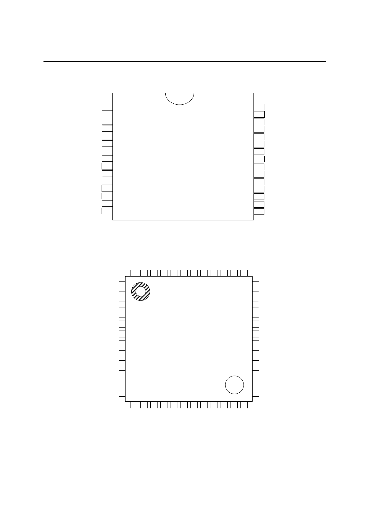
PIN CONFIGURATION (TOP VIEW)
VDD
SWA
SWB
SWC
AMPAI
AMPAO
AIN+
AIN–
GSX
SWD
SWE
SG
VFRO
AG1
SAO
1
2
3
4
5
6
7
8
9
10
11
12
13
14
15
NC
AMPAI
AMPAO
AIN+
AIN–
GSX
NC
NC
SWD
SWE
SG
NC
1
2
3
4
5
6
7
8
9
10
11
12
NC
48
13
NC
SWC
47
14
NC
30-Pin Plastic SSOP
SWA
45
16
AG1
DD
V
44
17
NC
NC
43
18
SAO
NC
42
19
A
V
DG
41
20
PWI
SWB
46
15
VFRO
NC: No Connection
48-Pin Plastic TQFP
MCK
40
21
NC
DEN
DIO
39
38
22
23
AOUT–
AOUT+
NC
37
24
NC
30
29
28
27
26
25
24
23
22
21
20
19
18
17
16
36
NC
35
EXCK
34
PCMOUT
33
PCMIN
32
SYNC
31
NC
30
BCLK
29
PDN
28
NC
27
AG2
26
NC
25
NC
MSM7732-01
DG
MCK
DEN
DIO
EXCK
PCMOUT
PCMIN
SYNC
BCLK
PDN
AG2
AOUT+
AOUT–
PWI
V
A
3/29
FEDL7732-01-10
OKI Semiconductor
8 7 6 5 4 3 2 1
H
G
F
E
D
C
B
A
AG2 AOUT+
PDN
BCLK NC
SYNC NC
PCMIN NC
PCMOUT
EXCK DIO
DEN MCK
NC
NC
AOUT- PWI
NC NC
NC NC
DG VDD
VA SAO
NC NC
NC NC
SWA SW B
Index (A1)
NC: No Connection
48-Pin Plastic LGA
48-Pin Plastic BGA
MSM7732-01
AG1 VFRO
SG SWE
NC SWD
NC GSX
NC AIN-
NC AIN+
NC AMPAO
SWC AMPAI
4/29

FEDL7732-01-10
OKI Semiconductor
PIN DESCRIPTION
Pin Symbol Type Description
1 VDD — Power supply (3.0 V)
2 SWA IO Analog switch A
3 SWB IO Analog switch B
4 SWC IO Analog switch C
5 AMPAI I Amplifier A inverting input
6 AMPAO O Amplifier A output
7 AIN+ I Transmit side amplifier non-inverting input
8 AIN– I Transmit side amplifier inverting input
9 GSX O Transmit side amplifier output
10 SWD IO Analog switch D
11 SWE IO Analog switch E
12 SG O Analog signal ground (1.4 V)
13 VFRO O Receive side voice output
14 AG1 — Analog ground 1 (0 V)
15 SAO O Receive side sounder amplifier output
16 VA — Analog power supply (3.0 V)
17 PWI I Receive side voice amplifier input
18 AOUT– O Receive side voice amplifier output –
19 AOUT+ O Receive side voice amplifier output +
20 AG2 — Analog ground 2 (0 V)
21
22 BCLK I PCM data shift clock input
23 SYNC I PCM data shift sync signal input
24 PCMIN I Receive side PCM signal input
25 PCMOUT O Transmit side PCM signal output
26 EXCK I Clock signal input for control register
27 DIO IO Address and data input or output for control register
28 DEN I Enable signal input for control register
29 MCK I Master clock input (2.048 MHz)
30 DG — Digital ground (0 V)
PDN
I Power down control input
MSM7732-01
5/29
FEDL7732-01-10
A
–
A
A
A
OKI Semiconductor
MSM7732-01
PIN FUNCTIONAL DESCRIPTION
AIN+, AIN–, GSX
Transmit analog inputs and the output for transmit gain adjustment.
AIN– connects to inverting input of the internal transmit amplifier. AIN+ connects to non-inverting input of the
internal transmit amplifier. GSX connects to the internal transmit amplifier output. Refer to Figure 1 for gain
adjustment.
VFRO, SAO, AOUT+, AOUT–, PWI
Receive analog outputs and the outputs for receive gain adjustment.
VFRO is the receive filter output for the voice signal. SAO is the receive filter out put for an acoustic component of
the sound tone. SAO can directly drive 32 Ω load. AOUT+ and AOUT– are differential analog signal outputs
which can directly drive a 32 Ω load. Refer to Figure 1.
R2
GSX
IN–
IN+
SG
OUT+
OUT–
PWI
VFRO
SAO
–
+
Transmit Gain:
V/Vi
–1
to ENCODER
VREF
D/A
Conv.
Vi
C1
R1
0.1 µF
10 µF
+
Vo = VVFRO (R3/R4) ×2
R3
R4
Sounder output signal
Figure 1 Analog Input/Output Interface
6/29

FEDL7732-01-10
OKI Semiconductor
MSM7732-01
SG
Analog signal ground.
The output voltage of this pin is approximately 1.4 V. Put the bypass capacitors (10 µF in parallel with 0.1 µF
ceramic type) between this pin and AG to get the specified noi se characteristics. During power-down, this output
voltage is 0 V.
AMPAI, AMPAO
Used for amplifier A. The pin AMPAI is connected to the amplifier A inverting input, and the pin AMPAO is
connected to the amplifier A output.
SWA, SWB, SWC
Used for the internal analog switch. The pin SWB connects to the pin SWA o r the pin SWC. This is controlled by
CR1-B1.
SWD, SWE
Used for the internal analog switch. The pin SWD connects to the pin SWE or not. This is controlled by CR1-B2.
V
, VA
DD
+3 V power supply for analog. V
is the digital power supply. VA is the analog power supply.
DD
Since these pins are separated in the device, connect them as close as possible on the PCB.
DG, AG1, AG2
Ground. DG is the digital system ground. AG1 and AG2 are connected to the analog system ground.
The DG pin must be kept as close as possible to AG1 and AG2 on the PCB.
PDN
Power down and reset control input.
When set to digital “0”, the system changes to the power down state and control registers are reset. Since the power
down mode is controlled by a logical OR wi th CR0-B5 of t he control re gister, set C R0-B5 to logi c “0” when usi ng
this pin.
Be sure to reset the control registers by executing this power down to keep this pin to digital “0” level for 200 ns or
longer after the power is turned on and V
exceeds 2.4 V.
DD
MCK
Master clock input.
The frequency must be 2.048 MHz. MCK can be asynchronous with SYNC and BCLK.
BCLK
Shift clock input for the PCM data.
The frequency is set in the range of 64 kHz to 2048 kHz.
7/29
FEDL7732-01-10
OKI Semiconductor
MSM7732-01
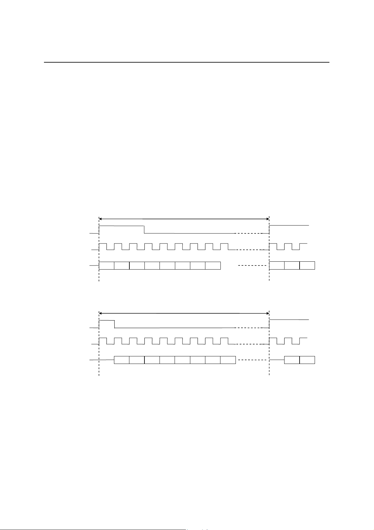
SYNC
8 kHz synchronous signal input for transmit and receive PCM data.
Synchronize this signal with BCLK signal. Refer to Figure 2.
PCMOUT
Transmit PCM data output.
This PCM output signal is output from MSB synchronously with the rising edge of BCLK and SYNC. Refer to
Figure 2. This is a logic o utput pin s o that external pull-up is not require d. This pin outputs logi c "L" except during
effective PCM data bits, and outputs logic "H" during power-down.
PCMIN
Receive PCM data input.
This PCM input signal is shifted in on the falling edge of BCLK and is input from MSB.
Refer to Figure 2.
SYNC
8 kHz (125 µs)
BCLK
PCMIN or
PCMOUT
MSB LSB
∗ 14 bit in the case of linear mode
(a) Long frame synchronous interface
8 kHz (125 µs)
SYNC
BCLK
PCMIN or
PCMOUT
MSB
LSB
∗ 14 bit in the case of linear mode
(b) Short frame synchronous interface
Figure 2 PCM Interface Basic Timing Diagram
8/29
FEDL7732-01-10
A
A
A
A0 A1A
OKI Semiconductor
MSM7732-01
DEN, EXCK, DIO
Serial control ports for MCU interface.
Reading and writing data is perf ormed by an external MCU through these pins. Eight registers with eight bits are
provided on the devices.
DEN is the "Enable" control signal input, EXCK is the data shift clock input, and DIO is the address and data input
or output. Figure 3 shows the input or output timing diagram.
DEN
EXCK
DIO
W
2
(a) Write Data Timing Diagram
0
1
B7
B6
B4 B5
B2B3
B1
B0
DEN
EXCK
DIO
R
B6
2
B7
B5
B4
B3
B2
B0 B1
input
(b) Read Data Timing Diagram
output
Figure 3 MCU Interface Input/Output Timing
Table 1 shows the register map.
Table 1
Name
CR0 0 0 0 A/µ SEL
CR1 0 0 1
CR2 0 1 0
CR3 0 1 1
CR4 1 0 0
CR5 1 0 1
CR6 1 1 0
CR7 1 1 1 VOX OUT
Address Control and Detect Data
A2 A1 A0 B7 B6 B5 B4 B3 B2 B1 B0
PON
AOUT
— — — —
TX
ON/OFF
Side Tone
GAIN2
DTMF/
OTHERS
ON/OFF
R/W : Read/Write enable R : Read only register
TX GAIN2 TX GAIN1 TX GAIN0
Side Tone
GAIN1
TONE
SEL
VOX
SEND
— — — — — — — —
ON LVL1 ON LVL0
TX NOISE
PDN ALL PDN TX PDN RX SLP SLP SEL LNR R/W
LVL1
Side Tone
GAIN0
SAO/
VFRO
TX NOISE
LVL0
SHORT
FRAME
ON/OFF
TONE
ON/OFF
TONE4 TONE3 TONE2 TONE1 TONE0 R/W
— — — — —
— — — — —
TONE
GAIN3
SW D/E SW C/A RX PAD R/W
RX
RX GAIN2 RX GAIN1 RX GAIN0 R/W
TONE
GAIN2
TONE
GAIN1
TONE
GAIN0
R/W
R/W
R/W
R/W
R
9/29

FEDL7732-01-10
OKI Semiconductor
MSM7732-01
ABSOLUTE MAXIMUM RATINGS
Parameter Symbol Condition Rating Unit
Power Supply Voltage VDD — –0.3 to +5.0 V
Analog Input Voltage V
Digital Input Voltage V
Storage Temperature T
— –0.3 to VDD+0.3 V
AIN
— –0.3 to VDD+0.3 V
DIN
— –55 to +150 °C
STG
RECOMMENDED OPERATING CONDITIONS
Parameter Symbol Condition Min. Typ. Max. Unit
Power Supply Voltage VDD Voltage must be fixed +2.4 +3.0 +3.3 V
Operating Temperature Ta — –40 — +85 °C
Input High Voltage VIH To all digital input pins 0.7 x V
Input Low Voltage VIL To all digital input pins 0 —
Digital Input Rise Time tir To all digital input pins — — 50 ns
Digital Input Fall Time tif To all digital input pins — — 50 ns
Digital Output Load CDL To all digital output pins — — 100 pF
Bypass Capacitor for SG CSG Between SG and AG 10+0.1 — — µF
Master Clock Frequency F
Bit Clock Frequency
Synchronous Signal Frequency F
Clock Duty Ratio D
MCK –0.01% 2.048 0.01% MHz
MCK
F
BCLK (A/µ-law) 64 — 2048 kHz
BCK1
BCLK (Linear) 128 — 2048 kHz
F
BCK2
SYNC — 8.0 — kHz
SYNC
MCK, BCLK, EXCK 40 50 60 %
CLK
TSB SYNC → BCLK -100 — 100 ns Sync Pulse Setting Time
BCLK → SYNC 100 — — ns
T
BS
Synchronous Signal Width tWS SYNC 1BCLK — 100 µs
— VDD V
DD
0.16 x
V
DD
V
10/29

FEDL7732-01-10
OKI Semiconductor
MSM7732-01
ELECTRICAL CHARACTERISTICS
DC Characteristics
(VDD = 2.4 V to 3.3 V, Ta = –40°C to +85°C)
Parameter Symbol Condition Min. Typ. Max. Unit
I
DD1
Power Supply Current
Input Leakage Voltage
I
DD2
I
DD3
IIH VI = VDD — — 2.0 µA
I
Output High Voltage VOH IOH = 0.4 mA 0.5 x V
Output Low Voltage VOL IOL = –1.2 mA 0 0.2 0.4 V
Input Capacitance CIN — — 5 — pF
Analog Interface Characteristics
Parameter Symbol Condition Min. Typ. Max. Unit
Input Resistance R
Output Load Resistance
Output Load Capacitance C
Output Amplitude
Total Harmonic Distortion
Input Offset Voltage
SG Output Voltage VSG SG — 1.4 — V
SG Output Impedance RSG SG — 40 80 kΩ
Internal Switch ON Impedance Rsw All internal switches — — 300 Ω
*1 –7.7 dBm (600Ω) = 0 dBm0 , +3.17 dBm0 = 1.3 VPP
2
*
Expected value
INX
R
LGX1
R
LGX2
LGX
VO1
VO2
2
VO3
*
THD1
2
THD2 AOUT+, AOUT– (VO3) — 1.0 — %
*
V
OFGX1
V
OFGX2
Operation Mode
No Signal (VDD = 3.0 V)
0 5.0 11.0 mA
Operation Mode
No Signal (V
= 3.0 V)
DD
0 9.0 20.0 mA
AOUT+, AOUT– or SAO is active
Power Down Mode
VI = 0 V — — 0.5 µA
IL
= 3.0 V, Ta = 25°C)
(V
DD
0 1.0 10 µA
— VDD V
DD
(VDD = 2.4 V to 3.3 V, Ta = –40°C to +85°C)
AMPAI, AIN+, AIN–, PWI 10 — — MΩ
AMPAO, GSX, VFRO 20 — — kΩ
SAO, AOUT+, AOUT– 32 — — Ω
Analog output pins — — 100 pF
AMPAO, GSX, VFRO RL = 20 kΩ
SAO RL = 32Ω
AOUT+, AOUT–
Differential output V
RL = 32Ω
AOUT+, AOUT–
Differential output V
RL = 30Ω
SAO, AOUT+, AOUT–(V
= 2.7 to 3.3 V
DD
= 3.0 V
DD
, VO2)
O1
— — *11.3 VPP
— — 3.0 VPP
— — 3.98 V
— — 1.0 %
AMPAO, GSX –20 — 20 mV
VFRO, SAO, AOUT+, AOUT– –100 — 100 mV
PP
11/29

FEDL7732-01-10
OKI Semiconductor
AC Characteristics
Parameter Symbol
Transmit Frequency Response
Receive Frequency Response
Transmit Signal to Distortion
Ratio
Receive Signal to Distortion
Ratio
Transmit Gain Tracking
Receive Gain Tracking
MSM7732-01
(VDD = 2.4 V to 3.3 V, Ta = –40°C)
Condition
Freq.
(Hz)
L
T1 0 to 60 25 — — dB
OSS
L
T2 300 to 3000 –0.15 — 0.20 dB
OSS
L
T3 1020 Reference dB
OSS
L
T4 3300 –0.15 — 0.80 dB
OSS
L
T5 3400 0 — 0.80 dB
OSS
L
R6 3968.75
OSS
L
R1 0 to 3000 –0.15 — 0.20 dB
OSS
L
R2 1020 Reference dB
OSS
L
R3 3300 –0.15 — 0.80 dB
OSS
L
R4 3400 0 — 0.80 dB
OSS
L
R5 3968.75
OSS
SD T1 3 35 — — dB
SD T2 0 35 — — dB
SD T3 –30 35 — — dB
1020
SD T4 –40 28 — — dB
SD T5
SD R1 3 35 — — dB
SD R2 0 35 — — dB
SD R3 –30 35 — — dB
1020
SD R4 –40 28 — — dB
SD R5
GT T1 3 –0.2 — 0.2 dB
GT T2 –10 Reference dB
GT T3 –40 –0.2 — 0.2 dB
1020
GT T4 –50 –0.6 — 0.6 dB
GT T5
GT R1 3 –0.2 — 0.2 dB
GT R2 –10 Reference dB
GT R3 –40 –0.2 — 0.2 dB
1020
GT R4 –50 –0.6 — 0.6 dB
GT R5
Level
Others
(dBm0)
0 —
0 —
(*1)
–45
(*1)
–45
—
–55
—
–55
Min. Typ. Max. Unit
13 — — dB
13 — — dB
23 — — dB
23 — — dB
–1.2 — 1.2 dB
–1.2 — 1.2 dB
12/29

FEDL7732-01-10
OKI Semiconductor
AC Characteristics (Continued)
Symbol
Parameter
N
Idle Channel Noise
IDLT
N
IDLR
AVT GSX 0.285
Absolute Signal Amplitude
A
VR
P
P
SRRT
SRRR
t
SDX
t
SDR
t
XD1
t
RD1
t
XD2
t
RD2
t
XD3
t
RD3
Power Supply Noise Rejection
Ratio
Digital Input/Output Timing PCM
Interface
tM1 50 — — ns
tM2 50 — — ns
tM3 50 — — ns
tM4 50 — — ns
Serial Port Digital Input/Output
Setting Time
tM5 100 — — ns
tM6 50 — — ns
tM7 50 — — ns
tM8 0 — 100 ns
tM9 50 — — ns
t
M10
t
M11
Shift Clock Frequency f
EXCK
*1 Use the P-message weighted filter.
*2 PCMIN input code "11010101"(A-law)
"11111111"(µ-law)
*3 0.320 Vrms = 0 dBm0 = –7.7 dBm
MSM7732-01
(VDD = 2.4 V to 3.3 V, Ta = –40°C to +85°C)
Condition
Freq.
(Hz)
Level
(dBm0)
Others
— AIN = SG (*1) — — –68
— — (*1,*2) — — –72
1020 0
30 — — dB
Noise Freq:
0 to 50 kHz
Noise
Level:
50 mVpp
VFRO 0.285
—
1 LSTTL
+
100 pF
See
Fig. 5
— CL
= 50 pF
See
Fig. 6
50 — — ns
— — EXCK — — 10 MHz
Min. Typ. Max. Unit
—
0.320
(*3)
0.320
(*3)
30 — — dB
0.359 Vrms
0.359 Vrms
0 — 200 ns
0 — 200 ns
0 — 200 ns
0 — 200 ns
0 — 50 ns
dBm0p
13/29

FEDL7732-01-10
/
/
OKI Semiconductor
MSM7732-01
AC Characteristics (DTMF and Other Tones)
(VDD = 2.4 V to 3.3 V, Ta = –40°C to +85°C)
Parameter Symbol Condition Min. Typ. Max. Unit
Frequency Difference DFT DTMF Tones, Other Tones –1.5 — +1.5 %
Transmit
Tones
(Gain setting
0 dB)
Receive
Tones
(Gain setting
–6 dB)
V
DTMF (High) and
DTMF (High) and
VTL,V
TH
DTMF (Low) –18 –16 –14 dBm0
Other Tones
DTMF (Low) –10 –8 –6 dBm0
Other Tones
V
RH
RL
–16 –14 –12 dBm0
–8 –6 –4 dBm0
+1 +2 +3 dB
Original (Reference) Tones
Signal Level *4
Relative Level of DTMF Tones R
VTL
VTH
VRL
V
RH
DTMF
*4 Does not include the setting value for the programmable gain.
AC Characteristics (Programmable Gain Stages)
(VDD = 2.4 V to 3.3 V, Ta = –40°C to +85°C)
Parameter Symbol Condition Min. Typ. Max. Unit
Gain Accuracy DG
All gain stages, to programmed value
–1 0 +1 dB
AC Characteristics (Voice Detect Function)
(VDD = 2.4 V to 3.3 V, Ta = –40°C to +85°C)
Parameter Symbol Condition Min. Typ. Max. Unit
Voice Detection Accuracy
TVON — 5 — ms Voice Detection Time
TVOF
DVX
Silence>Voice
(Voice/Silence differential: 10 dB)
For detection level set values by
CR6-B6, B5
140 160 180 ms
–2.5 0 2.5 dB
14/29

FEDL7732-01-10
OKI Semiconductor
TIMING DIAGRAM
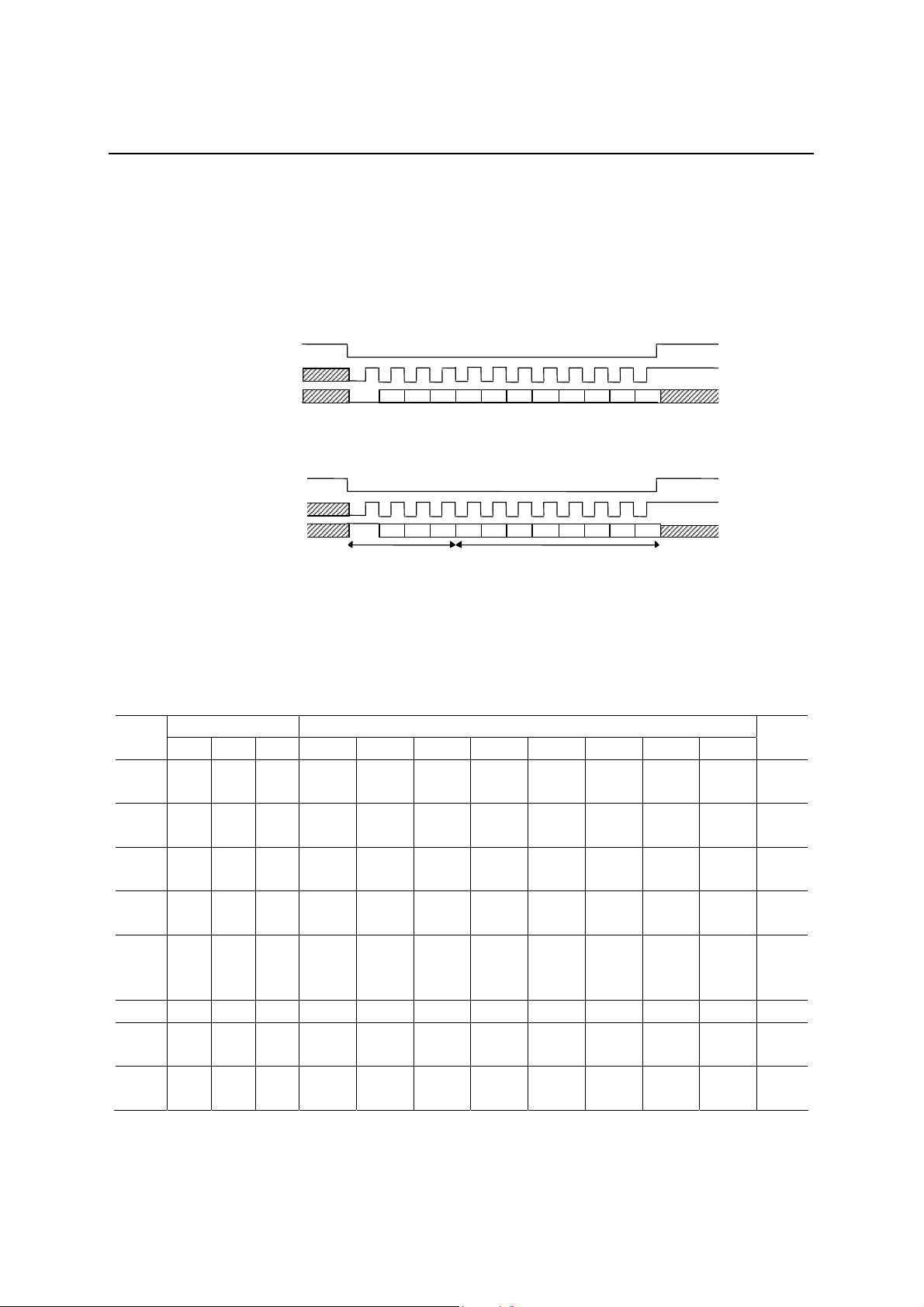
Transmit Side PCM Timing (Normal Synchronous Interface)
BCLK
0
t
SB
SYNC
PCMOUT
When tSB >= 0, the Delay of the MSB is defined as t
When t
Transmit Side PCM Timing (Short Frame Synchronous Interface)
BCLK
0
t
SB
SYNC
PCMOUT
Receive Side PCM Timing (Normal Synchronous Interface)
BCLK
0
t
SB
SYNC
PCMIN
Receive Side PCM Timing (Short Frame Synchronous Interface)
BCLK
0
t
SB
SYNC
PCMIN
1 2 3 4 5 6 7 8 9
t
WS
t
SDX
t
XD1
t
t
XD2
MSB
< 0, the Delay of the MSB is defined as t
SB
1 2 3 4 5 6 7 8 9
t
BS
WS
t
XD1
t
XD2
MSB
1 2 3 4 5 6 7 8 9
t
WS
t
RD1
t
RD2
MSB LSB
t
SDR
1 2 3 4 5 6 7 8 9
t
BS
t
WS
t
RD1
t
RD2
MSB
Figure 4 PCM Interface Timing
SDX
XD1
MSM7732-01
10
t
XD3
LSB
.
.
10
t
XD3
LSB
10
t
RD3
10
t
RD3
LSB
15/29

FEDL7732-01-10
A0A
A0 A1 A
A
OKI Semiconductor
Serial Port Timing for Microcontroller Interface
DEN
EXCK
DIO
(WRITE)
DIO
(READ)
tM2
2
1
t
t
M3
M1
t
W/R
W/R
M4
1
2
3
tM6
t
M5
1
Figure 5 Serial Control Port Interface
MSM7732-01
t
M10
12
11
5
4
t
M7
6
t
M9
B7
t
M8
B7
B1
B1
B0
B0
t
M11
16/29

FEDL7732-01-10
OKI Semiconductor
FUNCTIONAL DESCRIPTION
Control Registers
CR0 (Basic operating mode 1)
B7 B6 B5 B4 B3 B2 B1 B0
CR0 A/µ SEL
Initial Value 0 0 0 0 0 0 0 0
…………
B7
…………
B6
…………
B5
PCM companding law select; 0/µ-law, 1/A-law
Power on control for output amps (AOUT+, AOUT–); 0/Power down, 1/Power on
Power down (entire system); 0/Power on, 1/Power down
When using this data for power down control, set pin PDN at “1” level.
The control registers are not reset by this signal.
…………
B4
…………
B3
…………
B2
…………
B1
…………
B0
Power down (transmit and amplifier A); 0/Power on, 1/Power down
Power down (receive only); 0/Power on, 1/Power down
Slope filter enable; 0/Slope filter disable, 1/ Slope filter enable
The type of slope filter select; 0/CASE1, 1/CASE2, refer to Figure 6.
PCM interface linear code select;
0/Companding law selected by CR0-B7
1/14-bit linear code (2’s complement) in spite of CR0-B7
4
2
0
–2
[dB]
–4
Gain
–6
–8
–10
–12
–14
0 500 1000 1500 2000 2500 3000 3500 4000
Figure 6 Frequency Response of Slope Filter
PON
AOUT
PDN ALL PDN TX PDN RX SLP SLP SEL LNR
Frequency
MSM7732-01
Note: Initial Value: Reset state by PDN
CASE1
CASE2
[Hz]
17/29

FEDL7732-01-10
OKI Semiconductor
MSM7732-01
CR1 (Basic operating mode 2)
B7 B6 B5 B4 B3 B2 B1 B0
CR1 — — — —
Initial Value 0 0 0 0 0 0 0 0
SHORT
FRAME
SW D/E SW C/A RX PAD
B7, B6, B5, B4
…………………
B3
……
Not used
Short frame synchronous interface select;
0/Long frame synchronous interface, 1/Short frame synchronous interface
…………………
B2
…………………
B1
Analog switch control : 0/SWD to SWE open, 1/ SWD to SWE closed
Analog switch control : 0/SWB to SWA closed. The SWC pin is high impedance.
1/SWB to SWC closed. The SWA pin is high impedance.
…………………
B0
Receive side PAD : 1/inserted, 12 dB loss
0/no PAD
18/29

FEDL7732-01-10
OKI Semiconductor
MSM7732-01
CR2 (PCM CODEC operating mode setting and transmit/receive gain adjustment)
B7 B6 B5 B4 B3 B2 B1 B0
CR2 TX
ON/OFF
Initial Value 0 0 1 1 0 0 1 1
TX
GAIN2
TX
GAIN1
TX
GAIN0
RX
ON/OFF
RX
GAIN2
RX
GAIN1
RX
GAIN0
…………………
B7
B6, B5, B4
…………………
B3
B2, B1, B0
…………
…………
PCM coder disable; 0/Enable, 1/Disable (transmit PCM idle pattern)
Transmit gain adjustment, refer to Table 2.
PCM decoder disable; 0/Enable, 1/Disable (receive PCM idle pattern)
Receive gain adjustment, refer to Table 2.
Table 2
B6 B5 B4 Transmit Gain B2 B1 B0 Receive Gain
0 0 0 –6 d B 0 0 0 –1 2 d B
0 0 1 –4 d B 0 0 1 –9 dB
0 1 0 –2 d B 0 1 0 –6 dB
0 1 1 0 dB 0 1 1 –3 d B
1 0 0 +2 dB 1 0 0 0 d B
1 0 1 +4 dB 1 0 1 + 3 dB
1 1 0 +6 dB 1 1 0 + 6 dB
1 1 1 +8 dB 1 1 1 + 9 dB
The above gain settings table shows the transmit/receive voice signal gain settings and the transmit side gain
settings for DTMF tones and other tones. Tone signal transmission is enabled by CR4-B6, and the gain setting is
set to the levels shown below.
DTMF tones (low group):
–16 dBm0
DTMF tones (high group) and other tones: –14 dBm0
For example, if the transmit gain set value is set to +8 dB (B6, B5, B4) = (1, 1, 1), then the following tones appear
at the PCMOUT pin.
DTMF tones (low group):
–8 dBm0
DTMF tones (high group) and other tones: –6 dBm0
Gain setting for the side tone (path to the receive side from the transm it side) a nd the recei ve si de t one is provide d
by register CR3.
19/29

FEDL7732-01-10
OKI Semiconductor
MSM7732-01
CR3 (Side tone and other tone generator gain setting)
B7 B6 B5 B4 B3 B2 B1 B0
CR3
Initial Value 0 0 0 0 0 0 0 0
Side Tone
GAIN2
Side Tone
GAIN1
Side Tone
GAIN0
TONE
ON/OFF
TONE
GAIN3
TONE
GAIN2
TONE
GAIN1
TONE
GAIN0
B7, B6, B5
…………………
B4
B3, B2, B1, B0
…………
……
Side tone path gain setting, refer to Table 3.
Tone generator enable; 0/Disable, 1/Enable
Tone generator gain adjustment for receive side, refer to Table 4.
Table 3
B7 B6 B5 Side Tone Path Gain
0 0 0 OFF
0 0 1 –15 dB
0 1 0 –13 dB
0 1 1 –11 dB
1 0 0 –9 dB
1 0 1 –7 dB
1 1 0 –5 dB
1 1 1 –3 dB
Table 4
B3 B2 B1 B0 Tone Generator Gain B3 B2 B1 B0 Tone Generator Gain
0 0 0 0 OFF 1 0 0 0 –20 dB
0 0 0 1 –34 dB 1 0 0 1 –18 dB
0 0 1 0 –32 dB 1 0 1 0 –16 dB
0 0 1 1 –30 dB 1 0 1 1 –14 dB
0 1 0 0 –28 dB 1 1 0 0 –12 dB
0 1 0 1 –26 dB 1 1 0 1 –10 dB
0 1 1 0 –24 dB 1 1 1 0 –8 dB
0 1 1 1 –22 dB 1 1 1 1 –6 dB
The tone generator gain setting table for the receive side, as shown in Table 4, depends upon the following
reference levels.
DTMF tones (low group): –2 dBm0
DTMF tones (high group) and other tones: 0 dBm0
For example, when selecting –6 dB (B3, B2, B1, B0) = (1, 1, 1, 1) as a tone generator gain, the signal amplitude of
each DTMF tone on SAO or VFRO is as follows:
DTMF tones (low group): –8 dBm0
DTMF tones (high group) and other tones: –6 dBm0
20/29

FEDL7732-01-10
OKI Semiconductor
MSM7732-01
CR4 (Tone generator operating mode and frequency select)
B7 B6 B5 B4 B3 B2 B1 B0
CR4
Initial Value 0 0 0 0 0 0 0 0
DTMF/
Others SEL
TONE
SEND
SAO/
VFRO
TONE4 TONE3 TONE2 TONE1 TONE0
……………………
B7
……………………
B6
……………………
B5
DTMF or other tones select; 0/Others, 1/DTMF
Tone transmit enable (transmit side); 0/Voice signal (transmit), 1/Tone transmit
Tone output pin select (receive side); 0/VFRO, 1/SAO
B4, B3, B2, B1, B0 … Tone frequency setting, refer to Tables 5-1 and 5-2.
(a) B7 = 1 (DTMF tones)
Table 5-1
B4 B3 B2 B1 B0 Frequency B4 B3 B2 B1 B0 Frequency
* 0 0 0 0 697 Hz + 1209 Hz * 1 0 0 0 852 Hz + 1209 Hz
* 0 0 0 1 697 Hz + 1336 Hz * 1 0 0 1 852 Hz + 1336 Hz
* 0 0 1 0 697 Hz + 1477 Hz * 1 0 1 0 852 Hz + 1477 Hz
* 0 0 1 1 697 Hz + 1633 Hz * 1 0 1 1 852 Hz + 1633 Hz
* 0 1 0 0 770 Hz + 1209 Hz * 1 1 0 0 941 Hz + 1209 Hz
* 0 1 0 1 770 Hz + 1336 Hz * 1 1 0 1 941 Hz + 1336 Hz
* 0 1 1 0 770 Hz + 1477 Hz * 1 1 1 0 941 Hz + 1477 Hz
* 0 1 1 1 770 Hz + 1633 Hz * 1 1 1 1 941 Hz + 1633 Hz
*Undefined
(b) B7 = 0 (Other tones)
Table 5-2
B4 B3 B2 B1 B0 Frequency B4 B3 B2 B1 B0 Frequency
0 0 0 0 0
0 0 0 0 1
0 0 0 1 0
0 0 0 1 1 — 1 0 0 1 1 1477 Hz
0 0 1 0 0 — 1 0 1 0 0 1633 Hz
0 0 1 0 1 — 1 0 1 0 1 2000 Hz
0 0 1 1 0 — 1 0 1 1 0 2100 Hz
0 0 1 1 1 — 1 0 1 1 1 —
0 1 0 0 0 — 1 1 0 0 0 2400 Hz
0 1 0 0 1 400 Hz 1 1 0 0 1 —
0 1 0 1 0 440 Hz 1 1 0 1 0 2500 Hz
0 1 0 1 1 480 Hz 1 1 0 1 1 —
0 1 1 0 0 — 1 1 1 0 0 —
0 1 1 0 1 667 Hz 1 1 1 0 1 2700 Hz
0 1 1 1 0 800 Hz 1 1 1 1 0 —
0 1 1 1 1 1000 Hz 1 1 1 1 1 3000 Hz
2730 Hz/2500 Hz
8 Hz wamble
2000 Hz/2667 Hz
8 Hz wamble
1000 Hz/1333 Hz
8 Hz wamble
1 0 0 0 0 1200 Hz
1 0 0 0 1 1300 Hz
10010 —
21/29

FEDL7732-01-10
OKI Semiconductor
MSM7732-01
CR5 (Not used)
B7 B6 B5 B4 B3 B2 B1 B0
CR5
Initial Value 0 0 0 0 0 0 0 0
–– –– –– –– –– –– –– ––
………
B7-B0
Not used
CR6 (VOX function control)
B7 B6 B5 B4 B3 B2 B1 B0
CR6
Initial Value 0 0 0 0 0 0 0 0
VOX
ON/OFF
ON LVL1 ON LVL0
–– –– –– –– ––
………………………
B7
VOX function enable; 0/Disable, 1/Ena bl e
If B7 is set to a logic “1”, B3 should be set to a logic “1”.
……………………
B6, B5
Voice detector level setting;
(0,0): –20 dBm0 (0,1): –26 dBm0 (1,0): –32 dBm0 (1,1 ): –38 dBm0
B4, B2, B1, B0
………
Not used
CR7 (Detect register, read only)
B7 B6 B5 B4 B3 B2 B1 B0
CR7 VOX OUT
Initial Value 0 0 0 * * * * *
TX NOISE
LVL1
TX NOISE
LVL0
–– –– –– –– ––
*For IC testing
…………………………
B7
……………………
B6, B5
(0,0): Below –50 dBm0 (0,1): –40 to –50 dBm0
(1,0): –30 to –40 dBm0 (1,1): Above –30 dBm0
Note: These outputs are enabled when the VOX function is turned on by CR6-B7.
B4, B3, B2, B1, B0
………
Voice detection; 0/Silence, 1/Voice detect
Voice detect level (indicator);
Not used
22/29

FEDL7732-01-10
–GSX
P
A
A
OKI Semiconductor
APPLICATION CIRCUIT
Mic
GND
NC
48 47 46 45 44 43 42 41 40
NC
R1
C1
C4
R2
C2
R4
C3
C5
0.1 µF
AMPAI
AMPAO
AIN
R3
SWD
AIN+
NC
NC
SWE
10
SG
11
NC
12
1
2
3
20 kΩ
4
5
6
7
8
9
13 14 15 16 17 18 19 20 21
NC
SWC
20 kΩ
VREF
NC
SWB
A/D
20 kΩ
VFRO
C9
10 µF
SWA
Slope
Filter
D/A
AG1
V
V
NC
DD
DD
LPF
32
C6
MSM7732-01
32
MCK
Ω
NC
R6
C7
DEN
DIO
39 38 37
MCU I/F
PCM
Compand
TONE / DTMF
Gen
PCM
Expand
32
Ω
22 23 24
AOUT-
AOUT+
NC
NC
NC
36
EXCK
35
PCMOUT
34
PCMIN
33
SYNC
32
NC
31
BCLK
30
DN
29
NC
28
G2
27
NC
GND
26
NC
25
Earphone
IN
OUT
NC
NC
DG
Voic e
Detect
BPF
Ω
V
SAO
PWI
V
DD
R5
Hands Free Kit
Speake r
23/29

FEDL7732-01-10
OKI Semiconductor
PACKAGE DIMENSIONS
SSOP30-P-56-0.65-K
Mirror finish
MSM7732-01
(Unit: mm)
Package material Epoxy resin
Lead frame material 42 alloy
5
Pin treatment
Package weight (g) 0.19 TYP.
Rev. No./Last Revised 5/Dec. 5, 1996
Solder plating (≥5µm)
Notes for Mounting the Surface Mount Type Package
The surface mount type packages are very susceptible to heat in reflow mounting and humidity absorbed in st orage.
Therefore, before you perform reflow mounting, contact Oki’s resp onsible sales person for the product name,
package name, pin number, package code and desired mounting conditions (reflow method, temperature and
times).
24/29

FEDL7732-01-10
OKI Semiconductor
TQFP48-P-0707-0.50-K
MSM7732-01
(Unit: mm)
Mirror finish
Package material Epoxy resin
Lead frame material 42 alloy
5
Pin treatment
Package weight (g) 0.13 TYP.
Rev. No./Last Revised 4/Oct. 28, 1996
Solder plating (≥5µm)
Notes for Mounting the Surface Mount Type Package
The surface mount type packages are very susceptible to heat in reflow mounting and humidity absorbed in st orage.
Therefore, before you perform reflow mounting, contact Oki’s resp onsible sales person for the product name,
package name, pin number, package code and desired mounting conditions (reflow method, temperature and
times).
25/29

FEDL7732-01-10
OKI Semiconductor
P-LFBGA48-0707-0.80
MSM7732-01
(Unit: mm)
Package material Epoxy resin
5
Package weight (g) 0.12 TYP.
Rev. No./Last Revised 1/Jun. 20, 2001
Notes for Mounting the Surface Mount Type Package
The surface mount type packages are very susceptible to heat in reflow mounting and humidity absorbed in st orage.
Therefore, before you perform reflow mounting, contact Oki’s resp onsible sales person for the product name,
package name, pin number, package code and desired mounting conditions (reflow method, temperature and
times).
26/29

FEDL7732-01-10
OKI Semiconductor
P-TFLGA48-0707-0.80
MSM7732-01
(Unit: mm)
Package material Epoxy resin
5
Package weight (g) 0.10 TYP.
Rev. No./Last Revised 2/Jun. 20, 2001
Notes for Mounting the Surface Mount Type Package
The surface mount type packages are very susceptible to heat in reflow mounting and humidity absorbed in st orage.
Therefore, before you perform reflow mounting, contact Oki’s resp onsible sales person for the product name,
package name, pin number, package code and desired mounting conditions (reflow method, temperature and
times).
27/29

FEDL7732-01-10
g
X
OKI Semiconductor
MSM7732-01
REVISION HISTORY
Document
No.
FEDL7732-01-04 Nov. 2001 ― ― Edition 4
FEDL7732-01-05 Jan. 15, 2002
FEDL7732-01-06 Jun. 3, 2004 2 2 Addition of RX PAD in the Block Diagram.
FEDL7732-01-07 Jun. 15, 2004 8 8 More clarification of PCMOUT output state
FEDL7732-01-08 Jul. 29, 2004 23 23
FEDL7732-01-09 May 18, 2005 2 2
FEDL7732-01-10 Nov 2, 2005
Date
Previous
Page
ram
SB
Description
XD1
Current
Edition
26 26 Changed the package outline diagram.
27 27 Changed the package outline diagram.
10 10 Addition of tSB
15 15
Edition
Correction of false connection of C2 and R3 in
APPLICATION CIRCUIT
Addition of TXON/OFF and RXON/OFF in the
Block Dia
Addition of t
Addition of description about t
and t
SD
28/29

FEDL7732-01-10
OKI Semiconductor
MSM7732-01
NOTICE
1. The information contained herein can change without not i ce owing to product and/or te chnical improvements.
Before using the product, please make sure that the information being referred to is up-to-date.
2. The outline of action and examples for application circuits described herein have been chosen as an explanation
for the standard action and performance of the p roduct. When planning to use the product, please ensure that the
external conditions are reflected in the actual circuit, assembly, and program designs.
3. When designing your product, please use our product below the specified maximum ratings and within the
specified operating ranges including, but not limited to, operating voltage, power dissipation, and operating
temperature.
4. Oki assumes no responsibility or liability whatsoever for any failure or unusual or unexpected operation
resulting from misuse, neglect, improper installation, repair, alteration or accident, improper handling, or
unusual physical or electrical stress including, but not limited to, expo sure to p arameters beyond the specified
maximum ratings or operation outside the specified operating range.
5. Neither indemnity against nor license of a t hi rd party ’s industrial and intellectual property right, etc. is granted
by us in connection with the use of the product and/or the information and drawings contained herein. No
responsibility is assumed by us for any infringement of a third party’s right which may result from the use
thereof.
6. The products listed in this document are intended for use in general electronics equipment for commercial
applications (e.g., office automation, communication equipment, measurement equipment, consumer
electronics, etc.). These products are not, unless specifically authorized by Oki, authorized for use in any
system or application that requires special or enhanced quality and reliability characteristics nor in any system
or application where the failure of such system or application may result in the loss or damage of property, or
death or injury to humans.
Such applications include, but are not limited to, traffic and automotive equipment, safety devices, aerospace
equipment, nuclear power control, medical equipment, and life-support systems.
7. Certain products in this document may need government approval before they can be exported to particular
countries. The purchaser assumes the responsibility of determining the legality of export of these products and
will take appropriate and necessary steps at their own expense for these.
8. No part of the contents contained herein may be reprinted or reproduced without our prior permission.
Copyright 2005 Oki Electric Industry Co., Lt d.
29/29
 Loading...