OKI MSM7731-02GA Datasheet

FEDL7731-02-04
1
Semiconductor
This version: Jan. 2000
Previous version: Jan. 2000
MSM7731-02
Dual Echo Canceler & Noise Canceler with Dual Codec for Hands-Free
1/53
GENERAL DESCRIPTION
The MSM7731 is an IC device developed for portable, handsfree communication with built-in line echo canceler,
acoustic echo canceler, and transmission signal noise canceler. Built-in to the voice signal interface is a linear
CODEC for the analog interface on the acoustic-side, and a linear CODEC for the analog interface on the line-side.
On the line-side, in addition to the analog interface, there is also a µ-law PCM/16-bit linear digital interface.
Equipped with gain and mute controls for data transmission and reception, a µ-law PCM/16-bit linear digital
interface for memo recording and message output, and transfer clock and sync clock generators for digital
communication, this device is ideally suited for a handsfree system.
FEATURES
• Single 3 V Power Supply Operation (2.7 to 3.6 V)
• Built-in 2-channel (line and acoustic) echo canceler
Echo attenuation : 35 dB (typ.) for white noise
Cancelable echo delay time :
Line echo canceler + acoustic echo canceler : Tlined = 27 ms (max.)
Tacoud = 59 ms – Tlined (max.)
Acoustic echo canceler only : Tacoud = 59 ms (max.)
• Built-in transmission signal noise c anceler
Noise attenuation : 17 dB (typ.) for white noise
40 dB (typ.) for single tone
• Built-in 2-channel CODEC
Synchronous transmission and reception enables full duplex operation
• Built-in analog input gain amp stage (max. gain = 30 dB)
• Analog output configuration : Push-pull drive (can drive a 1.2 k
Ω
load
)
• Built-in transmit slope filter
• Digital interface coding formats : µ-law PCM, 16-bit linear (2's complement)
• Digital interface sync formats : Normal-sync, short-frame-sync
• Built-in digital transmission clock generators
Sync clock (S YNC) : 8 kHz output
Transmission clock (BCLK) : 64 kHz output (µ-law PCM)/128 kHz output (16-bit linear)
• Digital transmission rate
External input : 64 to 2048 kbps
Internal generation : 64 kbps (µ-law PCM)/128 kbps (16-bit linear)
• Fixed digital interface sync clock (SYNC) enables automatic power-down
• Master clock frequency : 19.2 MHz
Compatible with crystal oscillator and crystal
• Low power consumption
Operating mode : typ. 35 mA (when V
DD
= 3.0 V in a silent mode)
Power down operation : typ. 0.02 mA (when V
DD
= 3.0 V in a silent mode)
• Control by both the serial microcomputer interface and parallel port is possible
• Transmit/receive mute function, transmit/receive programmable gain setting
• Package : 64-pin plastic QFP (QFP64-P-1414-0.80-BK)(Product name: MSM7731-02GA)
FEDL7731-02-04
1
Semiconductor
MSM7731-02
2/53
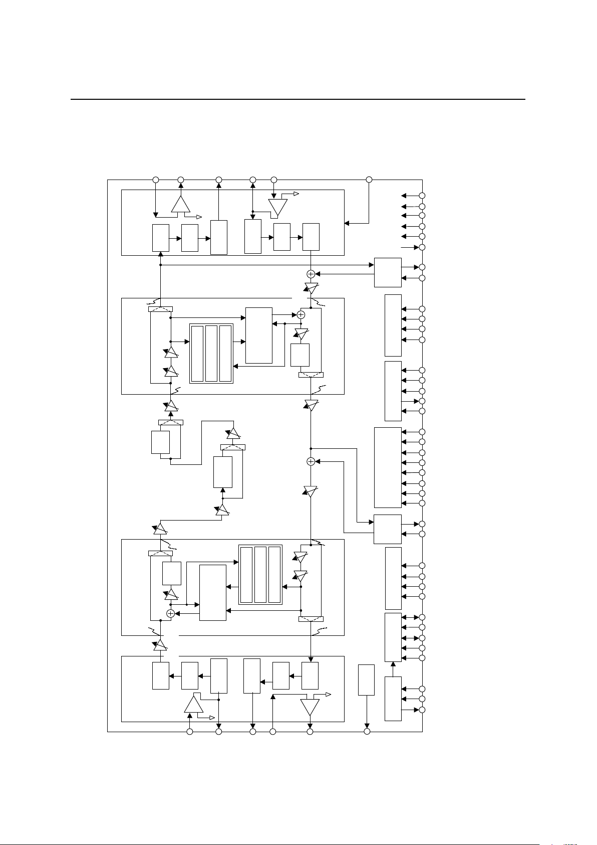
BLOCK DIAGRAM
AIN
AGSX
AVFRO
APWI
AOUT
SG
Linear Codec
(Acoustic side)
BPF
ADC
RC LPF
RC LPF
DAC
LPF
VREF
Clock Gen Timing Gen AEC Controller
P/S
&S/P
EC/NC/SF/PAD
Controller
MCU Interface LEC Controller
P/S
&S/P
–
+
–
+
1.2 k
Ω
LPADA
GPADA
GPADNC
RPAD GPADL
LPADNC
TPAD
ATTsA
Center
Chip
Power
Calc
.
Howling Detector
Double Talk Det
Acoustic
Adaptive
FIR
Filter
(
AAFF
)
RoutA
RinA
GainA ATTrA
SinA
SoutA
Slope
Filter
Noise
Canleler
ATTrL GainL
Power
Calc
.
Howling Detector
Double Talk Det
Line
Adaptive
FIR
Filter
(
LAFF
)
Center
Chip
RinL
RoutL
SinLSoutL
ATTsL
–
+
–
+
–
+
LPADL
LPWI
DAC
RC LPF
RC LPF
ADC
BPF
1.2 k
Ω
Acoustic Echo
Canceler
Line Echo
Canceler
Linear Codec
(Line side)
LOUT
LVFRO
LGSX
LIN
LINEEN
AGND
AVDD
DGND1,2
DVDD1,2
TEST1-4
TEST9
PCMO
PCMI
LTHR
LGC
LATT
LHD
D
EN
EXCK
DIN
DOUT
MCUSEL
NCPAD1,2
NCSEL1,2
RPAD1-4
TPAD1-4
ECSEL
GLPADTHR
SLPTHR
RST
PCMEO
PCMEI
ATHR
AGC
AATT
AHD
SYNC
SYNCSEL
BCLK
CLKSEL
PCMSEL
P
DN/RST
MCK/X1
X2
LPF
+
-
FEDL7731-02-04
1
Semiconductor
MSM7731-02
3/53
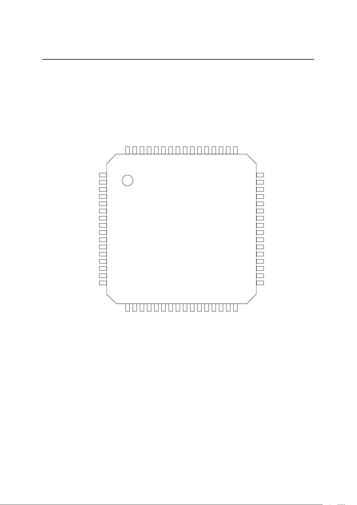
PIN CONFIGURATION (TOP VIEW)
64-Pin Plastic QFP
EXCK
DIN
NCSEL1
SLPTHR
TEST1
TEST2
TEST3
TEST4
NCSEL2
PDN/RST
RST
SYNC
BCLK
CLKSEL
PCMI
PCMEI
PCMEO
PCMO
PCMSEL
SYNCSEL
DOUT
DEN
DVDD2
GLPADTHR
TEST9
LINEEN
AGND
LOUT
LPWI
LVFRO
LGSX
LIN
48
47
46
45
44
43
42
41
40
39
38
37
36
35
34
33
646362616059585756555453525150
49
171819202122232425262728293031
32
1
2
3
4
5
6
7
8
9
10
11
12
13
14
15
16
RPAD2
RPAD1
DGND2
TPAD4
TPAD3
TPAD2
TPAD1
MCK/X1
X2
AVDD
AGS
X
AIN
AVFRO
APWI
AOU
T
SG
ECSEL
MCUSEL
AHD
NCPAD2
AATT
AGC
DGND1
ATHR
LHD
NCPAD1
LATT
LGC
LTHR
RPAD4
DVDD1
RPAD3
FEDL7731-02-04
1
Semiconductor
MSM7731-02
4/53
PIN FUNCTIONAL DESCRIPTION
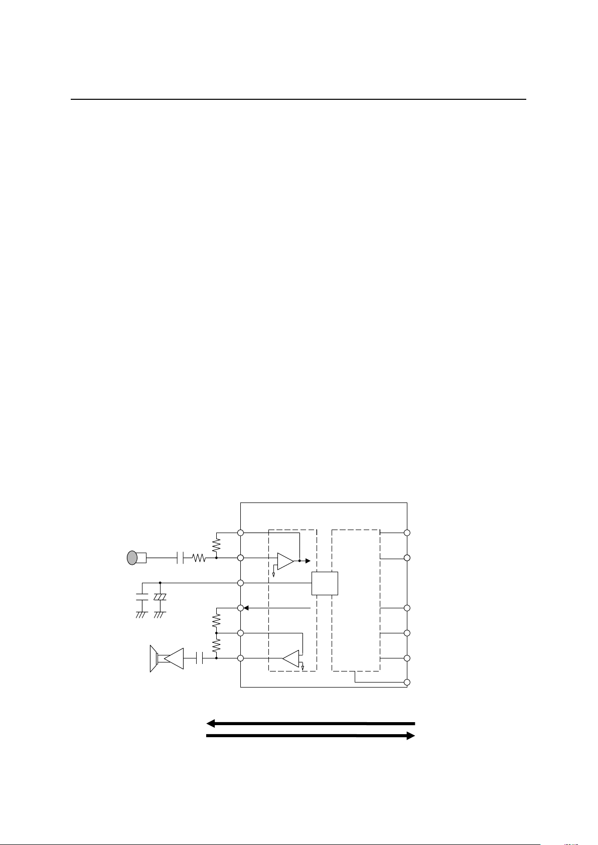
AIN, AGSX
These are the acoustic analog input and level adjusting pins. The A IN pin is conn ected to the inverting input of the
internal amp and the AGSX pin is connected to the amp output. For level adjustment, refer to the diagram below
(Figure 1). At power-down reset, the AGSX pin goes to a high impedance state.
AVFRO, AOUT, APWI
These are acoustic analog output and level adjusting pins. The AVFRO pin is an audio output and can directly
drive 20 kΩ. The AOUT pin is an analog output and can directly drive a load of 1.2 kΩ. For level adjustment, refer
to the diagram below (Figure 1). At power-down reset, these output pins go to a high impedance state.
LIN, LGSX
These are the line analog input and level adjusting pins. The LIN pin is connected to the inverting input of the
internal amp and the LGSX pin is connected to the amp output. For level adjustment, refer to the diagram below
(Figure 1). At power-down reset, the LGSX pin goes to a high impedance state. If LIN is not used, short the LIN
and LGSX together.
LVFRO, LOUT, LPWI
These are acoustic analog output and level adjusting pins. The LV FRO pin is an audio output and can directly drive
20 kΩ. The LOUT pin is an analog output and can directly driv e a load of 1.2 kΩ. For level adjustment, refer to the
diagram below (Figure 1). At power-down reset, these output pins go to a high impedance state. If LOUT is not
used, short the LPWI and LOUT pins together.
LINEEN
LINEENLINEEN
LINEEN
This is the power-down control pin for the line CODEC. A logic “0” continues normal operation and a logic “1”
power down only the line C ODEC. If the line CODEC is not used, pow er down the line CODEC and s hort th e LIN
pin to the LGSX pin and the LPWI pin to the LOUT pin. This procedure results in the low consumption of
electrical power. At power-down, the output pins go to a high impedance state. If the pin setting is changed, reset
must be activated by either the
PDN/RST
pin or the PDN/RS T bit (CR0-B7). This pin is ORed w ith CR0-B5 of th e
control register. Refer to the section “RELATIONSHIP BETWEEN PINS AND CONTROL REGISTERS”.
Figure 1 Analog Interface
Acoustic CODEC
C1
+
R1
MIC
0.1 µF
10 µF
–
R2
R3
R4
Line CODEC
V
AGSX
/Vi = R2/R1 ≤ 30
V
AGSX
= 1.3 V
PP
R2 ≥ 20 k
Ω
V
O/VAVFRO
= R4/R3 ≤ 2
V
O
= 2.6 VPP,
V
AVFRO
= 1.3 V
PP
R3, R4 ≥ 20 k
Ω
C2
SP
SPamp
Vo
Vi
AGSX
AIN
SG
AVFRO
APWI
AOUT
to ENCODER
LGSX
LIN
LVFRO
LPWI
LOUT
VREF
LINEEN
Receive Signal
Transmit Signal
Line Side (Hand Set)
Acoustic Side (Mic, Speaker)
Same as acoustic
analog interface
–
–
+
+
FEDL7731-02-04
1
Semiconductor
MSM7731-02
5/53
AGND
This is analog ground pin.
DGND1, DGND2
These are the digital ground pins.
AV
DD
This is the analog +3 V power supply pin.
DV
DD1
, DV
DD2
These are the digital +3 V power supply pins.
SG
This is the output pin for the analog signal ground potential. The output voltage is approximately 1.4 V.
Insert 10 µF and 0.1 µF ceramic bypass capacitors between the AGND and SG p in. At power-down rest, this
output becomes 0 V.
PDN
PDNPDN
PDN/RST
RSTRST
RST
This is the power-down reset control input pin. If a logic “0” is input to this pin, the device enters the power-down
state. At this time, all control register bits, internal variables, and coefficients of echo cancelers and noise cancelers
will be reset. After the power-down reset state is released, the device enters the initial mode (refer to the CR0
control register description). During normal operation, set this pi n to a logic “1”. The
PDN/RST
pin is ORed
(negative logic) with CR0-B7 of the control register. Refer to the section “RELATIONSHIP BETWEEN PINS
AND CONTROL REGISTERS”.
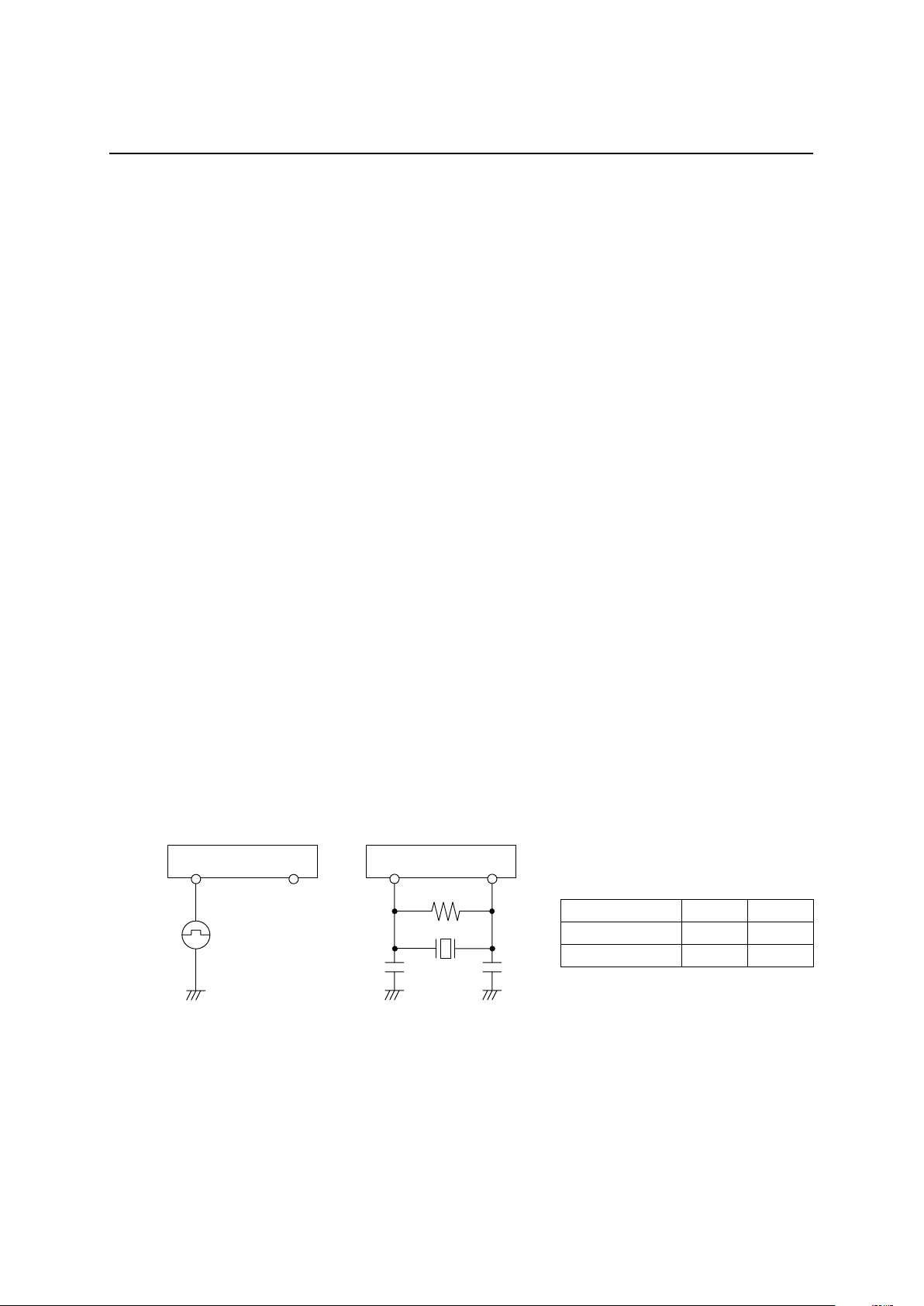
MCK/X1
This is the master clock input pin. The clock frequency is 19.2 MHz. The input clock may be asynchronous with
respect to the SYNC signal or the BCLK signal. Refer to Figure 2 (a) for an example application of an external
clock and Figure 2 (b) for an example oscillator circuit.
X2
This is the crystal oscillator output pin. If an existing external clock is to be used, leave this pin open and input the
clock to the MCK pin. Refer to Figure 2 (b) for an example oscillator circuit.
X’tal (19.2 MHz) C R
HC-49/U 10 pF 1 M
Ω
CX-91F T.B.D T.B.D
Figure 2 (a) External Clock Figure2 (b) Oscillator Circuit
Application Example Example
MCK/X1 X2
C
MCK/X1
X2
C
X’tal
R

FEDL7731-02-04
1
Semiconductor
MSM7731-02
6/53
SYNC
This is the 8 kHz sync signal I/O pin for digital data communication. This pin is switched to unction as an input or
output by the CLKSEL pin. If the internal clock mode is selected by the CLKSEL pin, an 8 kHz clock
synchronized to be BCLK signal is output and digital data communication is performed. If the external clock mode
is selected by the CLKSEL pin, this pin becomes an input that requires an 8 kHz clock input synchronized to be
BCLK pin, and digital data communication is performed based on this input clock. This pin enables automatic
power-down control. Fixing this pin to a logic “1” or logic “0” causes this device to enter the power-down state.
Two kinds of power-down modes can be selected by the SYPDN (CR11-B0) bit of the control register. For the
power-down mode, refer to the description of control register CR11.
BCLK
This is the shift clock I/O pin for digital data communication. This pin is switched to function as an input or output
by the CLKSEL pin. If the internal clock mode is selected by the CLKSEL pin, a 64 kHz or 128 kHz clock
synchronized to the SYNC signal is outp ut and digital data communication is p erformed. Switc hing between 6 4
kHz and 128 kHz is performed by the PCMSEL pin or PCMSEL (CR11-B1) bit. If µ-law PCM is selected by the
PCMSEL pin or PCMSEL bit, a 64 kHz clock is output. Or, if 16-bit linear mode is selected, a 128 kHz clock is
output. If the external clock mode is selected by the CLKSEL pin, this pin becomes an input that requires a clock
input synchronized to the SYNC. In this case, the clock frequency range is from 64 kHz to 2048 kHz.
CLKSEL
This pin selects internal or external clock modes for the SYNC and BCLK signals. A logi c “ 0” selects the intern al
clock mode. At this time, SYNC and BCLK pins are con figured as ou tput pins and each intern ally generated clock
is output to perform digital data communication. A logic “1” selects the external clock mode and configures the
SYNC and BCLK pins as input pins. At this time, digital data communication is performed with the externally
input SYNC and BCLK clocks. If digital data communication is not used, set this pin to a logic “0” to select
internal clocks. If the pin setting is changed, reset must be activated by either the
PDN/RST
pin or the PDN/RST
bit (CR0-B7).
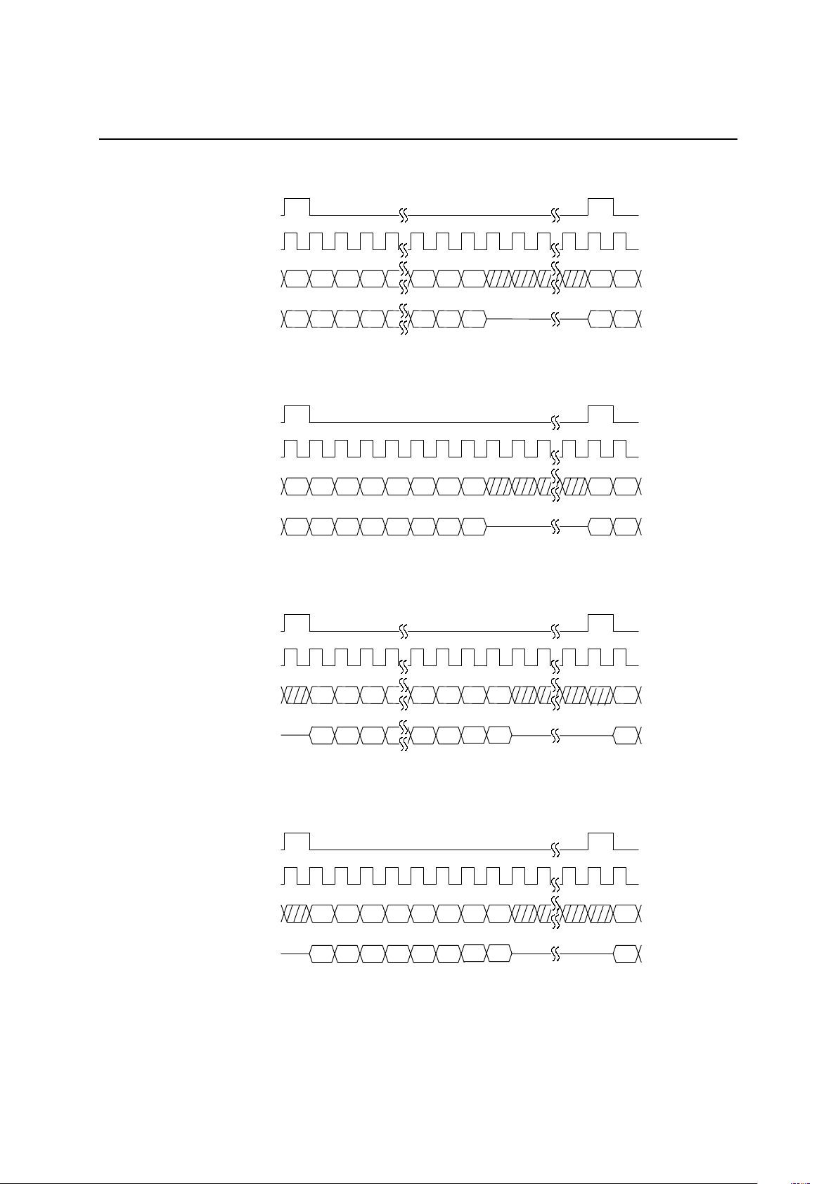
PCMI
This is the digital receive signal input pin on the line-side. This input signal is shifted at the rising edge of the
BCLK signal and input. The beginning of digital data is identified on the rising edge of the SYNC signal. The
coding format can be selected as µ-law PCM or 16-bit linear (2’s complement) by the PCMSEL pin or PCMSEL
(CR11-B1) bit. If the PCMI pin is not used, set it to a logic “1” if µ-law PCM has been selected, or a logic “0” if
16-bit linear mode has been selected. The sync format can be selected as normal-sync or short-frame-sync by the
SYNCSEL pin. Refer to Figure 3 for the timing. This digital input signal is added internally to the CODEC digital
output signal. Be careful of overflow when using the CODEC.
PCMO
This is the digital transmit signal output pin on the line-side. This output signal is synchronized to the rising edge
of the BCLK and SYNC signals and then output. Wh en not used f or output , this pin is in the h igh impedance state.
It is at high impedance during the power-down reset and the initial modes. The coding format can be selected as
µ
-law PCM or 16-bit linear (2’s complement) by the PCMSEL pin or PCMSEL (CR11-B1) bit. The sync format
can be selected as normal-sync or short-frame-sync by the SYNCSEL pin. Refer to Figure 3 for the timing.

FEDL7731-02-04
1
Semiconductor
MSM7731-02
7/53
PCMEI
This is the massage signal input pin. Use this pin when a massage is output to the speaker on the acoustic-side. This
input signal is shifted at the rising edge of the BCLK signal and then input. The beginning of digital data is
identified on the rising edge of the SYNC sign al. The coding format can be selected as µ-law PCM or 16-bit linear
(2’s complement) by the PCMSEL pin or PCMSEL (CR11-B1) bit. If the PCMEI pin is not used, set it to a logic
“1” if µ-law PCM has been selected, or a logic “0” if 16-bit linear m ode has been se lected. The sync format can be
selected as normal-sync or short-frame sync by the SYNCSEL pin. Timing is the same as for the PCMI pin (refer
to Figure 3). This dig i tal inpu t sign al is added internally to the echo can celer ou t put s ig n al. Be careful of overflow
during telephone conversations.
PCMEO
This output pin is for memo recording. Use it with the memo function. This output signal is synchron ized to the
rising edge of t he BCLK an SYNC signals a nd then output. When not used for output, this pin is in the high
impedance state. It is also at high impedance during the power-down reset and the initial modes. The coding format
can be selected as µ-law PCM or 16-bi t l inear (2’s complement) by the PCMSEL pin or PCMSEL (CR 11-B1) bit.
The sync format can be selected as normal-sync or short-frame-sync by the SYNCSEL pin. Timing is the same as
for the PCMO pin (refer to Figure 3).
SYNCSEL
This is the sync timing selection pin for digital data communication. A logic “0” selects normal-sync timing and a
logic “1” selects short-frame-sync timing. Refer Figure 3 for the timing. If the pin setting is changed, reset must be
activated by either the
PDN/RST
pin or the PDN/RST bit (CR0-B7)
PCMSEL
This is the coding format selection pin for digital data communication. A logic “1” selects µ-law PCM and a logic
“0” selects 16-bit linear (2’s complement) coding format. When an internal clock is selected, the BCLK signal
determines the output clock frequency. If the digital interface is not used, set this pin to logic “0” to select 16-bit
linear coding format.
If the pin setting is changed, reset must be performed by either the
PDN/RST
pin or the PDN/RST bit (CR0-B7).
This pin is logically ORed with the PCMSEL bit (CR11-B1). Refer to the section “RELATIONSHIP BETWEEN
PINS AND CONTROL REGISTERS”.
SLPTHR
This is the “through mode” control pin for the transmit slope filter. In the “through mode”, the filter is halted and
data is directly output. A logic “0” selects the normal mode (slope filter operation) and a logic “1” selects the
“through mode”. The slope filter decreases noises of low frequencies and improves speech quality. Refer to the
slope filter frequency characteristics. Because data is shifted into this pin in synchronization with the rising edge of
the SYNC signal, hold the data at the pin for 250 µs or longer. For further details, refer to the electrical
characteristics. This pin is ORed with the CR1-B1 bit of the control register. Refer to the section
“RELATIONSHIP BETWEEN PINS AND CONTROL REGISTERS”.
FEDL7731-02-04
1
Semiconductor
MSM7731-02
8/53
Figure 3 Digital Interface Timing
SYNC
(b) µ-law PCM coding format timing (normal sync)
BCLK
PCMI
PCMEI
PCMO
PCMEO
D7 D6 D5 D4 D3 D2 D1 D0 D7 D6
Hi-Z
D7 D6 D5 D4 D3 D2 D1 D0 D7 D6
SYNC
(a) 16-bit linear coding format timing (normal sync)
BCLK
PCMI
PCMEI
PCMO
PCMEO
D15 D14 D13 D12 D2 D1 D0 D15 D14
Hi-Z
D15 D14 D13 D12 D2 D1 D0 D15 D14
SYNC
(c) 16-bit linear coding format timing (short-frame sync)
BCLK
PCMI
PCMEI
PCMO
PCMEO
D15 D14 D13 D2 D1 D0 D15
D3
Hi-Z
D15 D14 D13 D2 D1 D0 D15
Hi-Z
D3
SYNC
(d) µ-law PCM coding format timing (short-frame sync)
BCLK
PCMI
PCMEI
PCMO
PCMEO
D7D7 D6 D5 D4 D3 D2 D1 D0
Hi-Z
D7D7 D6 D5 D4 D3 D2 D1 D0
Hi-Z

FEDL7731-02-04
1
Semiconductor
MSM7731-02
9/53
ECSEL
This is the echo canceler mode selection pin. A logic “1” selects the single echo canceler mode and a logic “0”
selects the dual echo canceler mode. If the pin setting is changed, reset must be activated by either the
PDN/RST
pin or the PDN/RST bit (CR0-B7). If the single echo canceler mode is selected, echo canceler control on the
line-side is unnecessary. This pin is ORed with the CR0-B0 bit of the control register. Refer to the section
“RELATIONSHIP BETWEEN PINS AND CONTROL REGISTERS”.
LTHR/ATHR
This is the “through mode” control pin for the echo canceler. In the “through mode”, SinL/A and RinL/A data is
directly output to SoutL/A and RoutL/A res pectively while each respective echo coefficient is maintained. A logic
“0” selects the normal mode (echo canceler operation) and a logic “1” selects the “through mode”. In the through
mode, the functions of HD, HLD, ATT and GC are inv alid. Because data is shifted in to this pin in syn chronization
with the rising edge of the SYNC signal, hold the data at the pin for 250 µs or longer. This pin is ORed with the
CR4-B7 and CR5-B7 bits of the control register. Refer to the section “RELATIONSHIP BETW EEN PINS AND
CONTROL REGISTERS”.
LHD
LHDLHD
LHD/AHD
AHDAHD
AHD
This pin turns ON or OFF the function to detect and cancel the howling that occurs in an acoustic system such as a
handsfree communication system. A logic “0” turns the function ON and a logic “1” turns the function OFF. This
function is valid when the LTHR/ATHR pin is in the normal mode. Because data is shifted into this pin in
synchronization with the rising edge of the SYNC signal, hold the data at the pin for 250 µs or longer. This pin is
ORed with the CR4-B4 and CR4-B4 and CR5-B4 bits of the control register. Refer to the section
“RELATIONSHIP BETWEEN PINS AND CONTROL REGISTERS”.
LATT
LATTLATT
LATT
This pin turns ON or OFF the ATT function to prevent howling by means of attenuators (ATTsL, ATTrL)
provided in the RinL inputs and SoutL outputs of the echo canceler. A logic “0” turns ON and a logic “1” turns
OFF the ATT function. If input is only to RinL, the ATTsL for SoutL is activated. If input is only to SinL, or if
there is input to both SinL and RinL, the ATTrL for RinL input is activated. The ATT value of each attenuator is
approximately 6 dB. This function is valid w h en the LTHR pin is in the n ormal mode. Becaus e data is shifted into
this pin in synchronization with the rising edge of the SYNC signal, hold the data at the pin for 250 µs or longer.
This pin setting is logically ORed with the CR4-B1 bit of the control register. Refer to the section
“RELATIONSHIP BETWEEN PINS AND CONTROL REGISTERS”.
AATT
AATTAATT
AATT
This is the ATT atlenuation selection pin to prevent howling by means of attenuators (ATTsA, ATTrA) provided
in the RinA inputs and SoutA outputs of the ech o can celer. A logic “ 0” selects 6 dB and a log ic “1” selects 12 dB.
If input is only to RinA, the ATTsA for SoutA is activated. If input is only to SinA, or if there is input to both SinA
and RinA, the ATTrA for RinA input is activated. This function is valid when the ATHR pin is in the normal m ode.
Because data is shifted into this pin in synchronization with the ris ing edge of the SYNC signal, h old the data at the
pin for 250 µs or longer. This pin setting is logically ORed with the CR5-B1 bit of the control register. Refer to the
section “RELATIONSHIP BETWEEN PINS AND CONTROL REGISTERS”.

FEDL7731-02-04
1
Semiconductor
MSM7731-02
10/53
LGC
LGCLGC
LGC/AGC
AGCAGC
AGC
This pin turns ON or OFF the gain control function to control the input level and prevent howling by means of gain
controls (GainL/A) provided in the RinL/A inputs of the echo canceler. The gain controller adjusts the RinL/A
input level when it is –10 dBm0 or above, and it has the control range of 0 to –8.5 dB. A logic “0” turns the
function ON and a logic “1” turns the function OFF. This functio n is valid when the LTHR/ATHR p in is in the
mormal mode. Because data is shifted into this pin in synchronization with the rising edge of the SYNC signal,
hold the data at the pin for 250 µs or longer. This pin is ORed with the CR4-B0 and CR5-B0 bits of the control
register. Refer to the section “RELATIONSHIP BETWEEN PINS AND CONTROL REGISTERS”.
Notes:
Lxx/Axx : In the above, Lxx refers to line echo canceler control pins and Axx to acoustic echo canceler control
pins.
xxL/xxA : In the above pin descriptions, xxL refers to line echo canceler functions and xxA to acoustic echo
canceler functions.
GLPADTHR
GLPADTHRGLPADTHR
GLPADTHR
This is the mode control pin for the attenuators (LPADL/A) provided in the SinL/A inputs and the amplifiers
(GPADL/A) provided in the SoutL/A outputs of the echo canceler. A logic “0” selects the “through mode” and a
logic “1” selects the normal m ode (PAD operation). The l evels are s et by t he CR10 regis ter. Settings of ± 18, ± 12,
± 6 and 0 dB are possible. The default setting is ± 12 dB. If the echo return loss (value of returned echo) is
amplified, set the LPAD level such that echo return loss will be attenuated. It is recommended to set the GPAD
level to the positive level equal to the LPAD level. If the pin se tting is changed, the coefficient reset must be
activated by either the
RST
pin or the RST bit (CR0-B6). Because data is shifted into this pin in synchronization
with the rising edge of the SYNC signal, hold the data at the pin for 250 µs or longer. This pin is ORed with the
CR1-B2 bit of the control register. Refer to the section “REL ATIONSHIP BET WEEN PINS AND CONTROL
REGISTERS”.
RST
RSTRST
RST
This input pin resets coefficients of the echo canceler and noise canceler. A logic “0” causes the reset state to be
entered. At this time, the filter coefficients for the echo canceler and noise canceler are reset. Control register
contents are preserved. While reset is being processed, there is not sound. During normal operation, set this pin to
a logic “1”. Use this pin in cases where the echo path changes (due to line switching during a telephone
conversation, etc.), or when resuming telephone communication. Because data is shifted into this pin in
synchronization with the rising edge of the SYNC signal, hold the data at the pin for 250 µs or longer. This pin is
ORed (negative logic) with the CR0-B6 bit of the control register. Refer to the section “RELATIONSHIP
BETWEEN PINS AND CONTROL REGISTERS”.
FEDL7731-02-04
1
Semiconductor
MSM7731-02
11/53
NCSEL1, NCSEL2
These are the noise attenuation selection pins. In the “through mode” the noise canceler is halted and data is
directly output. In the “normal mode” the noise canceler operates normally. Since the noise attenuation in the
normal mode is selected after the initial mode has been released, the change of the noise attenuation during normal
operation is invalid. If the noise attenuation is changed, reset must be activated b y the
RDN/RST
pin or the
PDN/RST bit (CR0-B7). Changing t o the through mode during normal operati on and returning to the normal mode
are possible. The NCSEL1 pin is ORed with the CR1-B0 bit of the control register and the NCSEL2 pin is ORed
with the CR12-B2 bit of the control register. Refer to the section “RELATIONSHIP BETW EEN PINS AND
CONTROL REGISTERS”.
Note:
Since there is a trade-off between noise attenuation and sound quality after canceling the noise, select the noise
attenuation appropriate to the sound quality.
NCSEL2 NCSEL1 NC Mode Attenuation (dB) Quality
0 0 Normal Mode 17 Better
1 1 Normal Mode 13.5
1 0 Normal Mode 8 Best
0 1 Through Mode — —
NCPAD1, NCPAD2
These are the noise canceler I/O gain adjusting pins. The gain adjustment is valid for tone control after canceling
the noise. The bigger the input level of the noise canceler is, the better the sou nd quality is. T he NCPAD1 pin is
ORed with the CR4-B2 bit of the con trol register and th e NCPAD2 pin is OR ed w ith the CR5-B2 bit of the control
register. Refer to the section “RELATIONSHIP BETWEEN PINS AND CONTROL REGISTERS”.
NCPAD2 NCPAD1 GPADNC (dB) LPADNC (dB)
0000
016–6
1 0 12 –12
1 1 18 –18
DEN
DENDEN
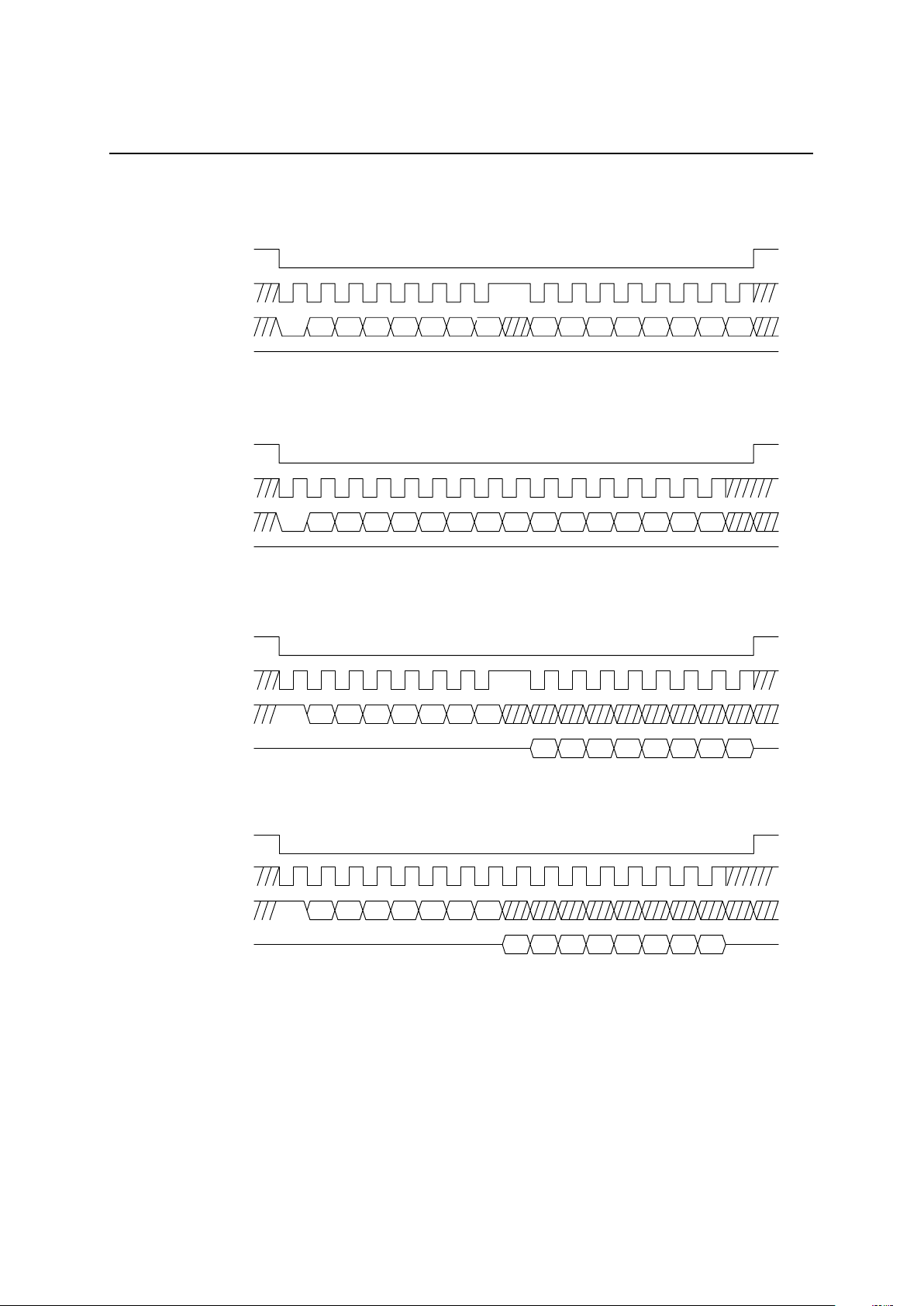
DEN, EXCK, DIN, DOUT
This is the serial port for the microcontroller interface. 13 bytes of control registers are provided in this IC dev ice.
There pins are used to write and read data from an external microcontroller. The
DEN
pin is an enable signal input
pin, the EXCK pin is a clock signal inp ut pin for data shifting, t he DIN pin is an addr ess and data input pin, the
DOUT pin is a data output pin. If the mirrocontroller interface is not used, set the
DEN
pin to a logic “1” and the
EXCK and DIN pins to a logic “0”. In addition, use the MCUSEL pin to specify the “unused” setting of the
microcontroller interface. Figure 4 shows the input timing.
MCUSEL
This pin selects whether the microcontroller interface is used or unused. A logic “0” specifies that the
microcontroller interface is used and a logic “ 1” specifies that it is not used. If the microcontroller interface is not
used, this pin must be set to a logic “1”. This pin is ORed with the CR0-B1 bit of the control register. Refer to the
section “RELATIONSHIP BETWEEN PINS AND CONTROL REGISTERS”.
↔
FEDL7731-02-04
1
Semiconductor
MSM7731-02
12/53
Figure 4 Microcontroller Interface I/O Timing
W A6A5A4A3A2A1A0 B7B6B5B4B3B2B1B0
12345678 910111213141516
DEN
EXCK
DIN
DOUT
(a) Data Write Timing 1 (8-bit MCU)
Hi-Z
W
A6 A5 A4 A3 A2 A1 A0 B7 B6 B5 B4 B3 B2 B1 B0
12345678910111213141516
(b) Data Write Timing 2 (16-bit MCU)
Hi-Z
DEN
EXCK
DIN
DOUT
R A6A5A4A3A2A1A0
B6 B5 B4 B3 B2 B1 B0B7
12345678 910111213141516
(c) Data Read Timing 1 (8-bit MCU)
Hi-Z Hi-Z
DEN
EXCK
DIN
DOUT
(d) Data Read Timing 2 (16-bit MCU)
123456789
10 11 12 13 14 15 16
R A6A5A4A3A2A1A0
B6 B5 B4 B3 B2 B1 B0B7
Hi-Z Hi-Z
DEN
EXCK
DIN
DOUT
FEDL7731-02-04
1
Semiconductor
MSM7731-02
13/53
RPAD4, RPAD3, RPAD2, RPAD1
These are the receive signal gain adjusting and mute setting pins. Refer to Table 1 for the settings. Set these pins to
a logic “0” when controlling by the control register. Because data is shifted into this pin in synchronization with the
rising edge of the SYNC signal, hold the data at the pin for 250 µs or longer. For further details, refer to the
electrical characteristics. These pins are ORed with the CR2-B3, B2, B1 and B0 bits of th e con trol reg ister. R ef er
to the section “RELATIONSHIP BETWEEN PINS AND CONTROL REGISTERS”.
TPAD4, TPAD3, TPAD2, TPAD1
These are the transmit signal gain adjusting and mute setting pins. Refer to Table 1 for the settings. Set these pins
to a logic “0” when controlling by the control register. Becau se data is shifted into this pin in synchronization w ith
the rising edge of the SYNC signal, hold the data at the pin for 250 µs or longer. For further details, refer to the
electrical characteristics. These pins are ORed with the CR3-B3, B2, B1 and B0 bits of th e con trol reg ister. R ef er
to the section “RELATIONSHIP BETWEEN PINS AND CONTROL REGISTERS”.
Table 1 RPAD/TPAD Setting
RPAD4 RPAD3 RPAD2 RPAD1 TPAD4 TPAD3 TPAD2 TPAD1 Level
0111 011121 dB
0110 011018 dB
0101 010115 dB
0100 010012 dB
0011 00119 dB
0010 00106 dB
0001 00013 dB
0000 00000 dB
1111 1111–3 dB
1110 1110–6 dB
1101 1101–9 dB
1100 1100–12 dB
1011 1011–15 dB
1010 1010–18 dB
1001 1001–21 dB
1000 1000MUTE
TEST1-4
Test inputs. Set these pins to a logic “0”.
TEST9
Test output.
FEDL7731-02-04
1
Semiconductor
MSM7731-02
14/53
ABSOLUTE MAXIMUM RATINGS
Parameter Symbol Condition Rating Unit
Power Supply Voltage V
DD
— –0.3 to +5.0 V
Digital Input Voltage V
IN
— –0.3 to VDD+0.3 V
Digital output Voltage V
OUT
— –0.3 to VDD+0.3 V
Storage Temperature T
STG
— –55 to +150 °C
RECOMMENDED OPERATING CONDITION
Parameter Symbol Condition Min. Typ. Max. Unit
Power Supply Voltage V
DD
— 2.7 — 3.6 V
Operating Temperature T
a
— –40 +25 +85 °C
SYNC, BCLK input pins 0.5×V
DD
MCK/X1 input pin 0.65×V
DD
Input High Voltage V
IH
Other digital input pins 0.45×V
DD
—VDDV
MCK/X1 input pin 0.35×V
DD
Input Low Voltage V
IL
Other digital input pins
0—
0.16×V
DD
V
Digital Input Rise Time t
IR
All digital inputs — — 20 ns
Digital Input Fall Time t
If
All digital inputs — — 20 ns
Master Clock Frequency f
MCK
MCK/X1 –100 ppm +19.2 +100 ppm MHz
Master Clock Duty Ratio D
MCK
MCK/X1 40 50 60 %
Bit Clock Frequency f
BCK
BCLK (during output) 64 — 2048 kHz
Bit Clock Duty Ratio D
CK
BCLK (during output) 40 50 60 %
Synchronous Signal
Frequency
f
SYNC
SYNC (during output) –100 ppm 8 +100 ppm kHz
Synchronous Signal Width t
WS
SYNC (during output) 1 BCLK — 100 ns
t
BS
BCLK to SYNC
(during input)
100 — — ns
Transmit/Receive Sync
Signal Setting Time
t
SB
SYNC to BCLK
(during input)
100 — — ns
R
DL
DOUT, PCMO, PCMEO 1 — — k
Ω
C
DL1
DOUT, PCMO, PCMEO — — 50 pF
Digital Output Load
C
DL2
SYNC, BCLK
(during output)
— — 20 pF
Bypass Condenser for SG C
SG
SG to AG 10+0.1 — — µF
FEDL7731-02-04
1
Semiconductor
MSM7731-02
15/53
ELECTRICAL CHARACTERISTICS
DC Characteristics
(VDD = 2.7 to 3.6 V, Ta = –25 to +85°C)
Parameter Symbol Condition Min. Typ. Max. Unit
Power Supply Current 1 I
DD1
Operating, no signal
(V
DD
= 3.0 V)
—3550mA
Power Supply Current 2 I
DD2
Power down mode
(V
DD
= 3.0 V, MCK = 0 V)
—0.02 1 mA
I
IH
VI = V
DD
—— 2 µA
Input Leakage Current
I
IL
VI = 0 V — — 2 µA
High Level Digital Output
Voltage
V
OH
IOH = 0.4 mA
(other than ×2)
0.5×V
DD
—VDDV
Low Level Digital Output
Voltage
V
OL
IOL = 3.2 mA
(other than ×2)
—0 0.2 0.4 V
Digital Output Leakage
Current
I
O
DOUT, PCMO, PCMEO — — 10 µA
Input Capacitance C
IN
——5—pF
Analog Interface Characteristics
(VDD = 2.7 to 3.6 V, Ta = –25 to +85°C)
Parameter Symbol Condition Min. Typ. Max. Unit
R
INA
AIN, APWI 10 — — M
Ω
Input Resistance
R
INL
LIN, LPWI 10 — — M
Ω
R
LA1
AGSX, AVFRO 20 — — k
Ω
R
LA2
AOUT 1.2 — — k
Ω
R
LL1
LGSX, LVFRO 20 — — k
Ω
Output Load Resistance
R
LL2
LOUT 1.2 — — k
Ω
C
LA1
AGSX, AVFRO, AOUT — — 100 pF
Output Load Capacitance
C
LL1
LGSX, LVFRO, LOUT — — 100 pF
V
OA1
AGSX,
AVFRO
R
L
= 20 k
Ω
——1.3Vpp
V
OA2
AOUT RL = 1.2 k
Ω
——2.6Vpp
V
OL1
LGSX,
LVFRO
R
L
= 20 k
Ω
——1.3Vpp
Output Voltage Level (*1)
V
OL2
LOUT RL = 1.2 k
Ω
——2.6Vpp
V
OFA1
AVFRO –100 — +100 mV
V
OFA2
AOUT –20 — +20 mV
V
OFL1
LVFRO –100 — +100 mV
Offset Voltage
V
OFL2
LOUT –20 — +20 mV
SG Output Voltage V
SG
SG — 1.4 — V
SG Output Impedance R
SG
SG — 40 80 k
Ω
Note*1: 0.320 Vrms = 0 dBm0, +3.14 dBm0 = 1.30 V
PP
FEDL7731-02-04
1
Semiconductor
MSM7731-02
16/53
Digital Interface Characteristics (1/3)
(VDD = 2.7 to 3.6 V, Ta = –25 to +85°C)
Parameter Symbol Condition Min. Typ. Max. Unit
PDN/RST
pin 1
Power-down/Reset Signal
Pulse Width
t
RSTW
PDN/RST control bit 1.6
——µS
Power-down/Reset Start
Time
t
PDND
PDN/RST
pin and
PDN/RST control bit
— — 50 nS
Power down/Reset End Time t
PDNH
PDN/RST
pin and
PDN/RST control bit
— — 200+
α
mS
Power-down/Reset Internal
Setting Time
t
PDNS
SYNC pin (input mode) 140 — 180 µS
Control Pulse Width t
PARW
250 — — µS
Control Start Time t
PARD
— — 250 µS
Control End Time t
PARH
(*2)
— — 250 µS
α
: Crystal activation
PDN/RST Timing
PDN/RST set timing
Control Timing (*2)
Note*2: Applies to the following pins/control bits:
LINEEN
, SLPTHR, NCTHR,
GLPADTHR
, TPAD6-1, RPAD6-1,
RST
, ATHR,
AATT
, AHLD,
AHD, AGC
, LTHR,
LATT
, LHLD,
LHD, LGC
pins, and control bits.
Power Down
Initial Mode
Hi-Z
t
PDND
t
PDNH
T
RSTW
PDN/RST
pin
PDN/RST control bi
t
Internal Operation
PCMO, PCMEO
SYNC (Ext. clock)
BCLK (Ext. clock)
PDN/RST control bit
(
Internal Write
)
t
PDNS
Internal processing
t
PARD
t
PARH
t
PARW
Pin/control bit
Internal operation
 Loading...