

OKI MSM7731-01GA Datasheet

E2U0060-18-84
Preliminary
¡ Semiconductor MSM7731-01
This version: Aug. 1998
¡ Semiconductor
MSM7731-01
Multifunction PCM CODEC (Voice Signal Processor)
GENERAL DESCRIPTION
The MSM7731 is an LSI device developed for portable, handsfree communication with built-in
line echo canceler, acoustic echo canceler, and transmission signal noise canceler. Built-in to the
voice signal interface is a linear CODEC for the analog interface on the acoustic-side, and a linear
CODEC for the analog interface on the line-side. On the line-side, in addition to the analog
interface, there is also a m-law PCM/16-bit linear digital interface.
Equipped with gain and mute controls for data transmission and reception, a m-law PCM/16bit linear digital interface for memo recording and message output, and transfer clock and sync
clock generators for digital communication, this device is ideally suited for a handsfree system.
FEATURES
• Single 3 V power supply operation (2.7 V to 3.6 V)
• Built-in 2-channel (line and acoustic) echo canceler
Echo attenuation : 35 dB (typ.)
Cancelable echo delay time :
Line echo canceler + acoustic echo canceler : Tlined = 27 ms (max.),
Tacoud = 59 ms – Tlined (max.)
Acoustic echo canceler only : Tacoud = 59 ms (max.)
• Built-in transmission signal noise canceler
Noise attenuation: 13 dB (typ.) for white noise
40 dB (typ.) for single tone
• Built-in 2-channel CODEC
Synchronous transmission and reception enables full duplex operation
• Built-in analog input gain amp stage (max. gain = 30 dB)
• Analog output configuration: Push-pull drive (can drive a 1.2 kW load)
• Built-in transmit slope filter
• Digital interface coding formats: m-law PCM, 16-bit linear (2's complement)
• Digital interface sync formats: Normal-sync, short-frame-sync
• Built-in digital transmission clock generators
Sync clock (SYNC): 8 kHz output
Transmission clock (BCLK): 64 kHz output (m-law PCM)/128 kHz
output (16-bit linear)
• Digital transmission rate
External input: 64 kbps to 2048 kbps
Internal generation: 64 kbps (m-law PCM)/128 kbps (16-bit linear)
• Fixed digital interface sync clock (SYNC) enables automatic power-down
• Master clock frequency: 19.2 MHz
Compatible with crystal oscillator and crystal
• Low power consumption
Operating mode: typ. 105mW (when VDD = 3.0 V)
Power-down mode: typ. 0.3mW (when VDD = 3.0 V)
• Control by both the serial microcomputer interface and parallel port is possible
• Transmit/receive mute function, transmit/receive programmable gain setting
• Package: 64-pin plastic QFP (QFP64-P-1414-0.80-BK) (Product name: MSM7731-01GA)
1/43
2/43
¡ Semiconductor MSM7731-01
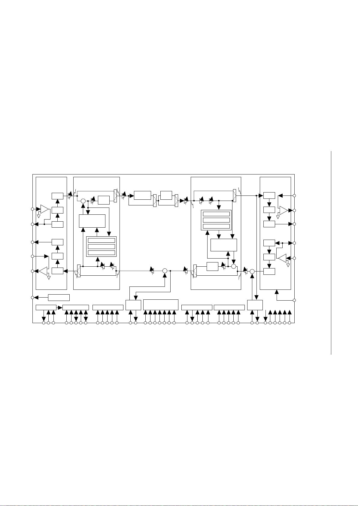
BLOCK DIAGRAM
TEST9
AGND
AVDDDGND1, 2
DV
DD1, 2
TEST1-4, 8
PCMO
PCMI
P/S
& S/P
LINEEN
LIN
LGSX
LVFRO
RC LPF
RC LPF
ADC
BPF
LPF
DAC
LOUT
LPWI
+
–
1.2kW
Linear CODEC
(Line side)
Power Calc.
Howling Detector
Double Talk Det
+
–
ATTsL
SinL
SoutL
+
+
Center
Clip
Line Adaptive
FIR Filter
(LAFF)
GainLATTrL
RinL
RoutL
Line Echo Canceler
TPAD
Slope
Filter
Noise
Canceler
SoutA
STTsA
+
–
+
Acoustic Adaptive
FIR Filter
(AAFF)
LPADA
SinA
Power Calc.
Howling Detector
Double Talk Det
ATTrA
RoutA
GainA
RinA
RPAD
+
Acoustic Echo Canceler
+
–
+
–
+
–
DAC
RC LPF
1.2kW
RC LPF
ADC
BPF
Linear CODEC
(Acoustic side)
APWI
AVFRO
AGSX
AOUT
AIN
V
REF
SG
LEC Controller
LTHR
LGC
LATT
LHLD
LHD
MCU Interface
DEN
EXCK
DIN
DOUT
MCUSEL
EC/NC/SF/PAD
Controller
RPAD1-4
TPAD1-4
ECSEL
GLPADTHR
NCTHR
SLPTHR
RST
PCMEO
P/S
& S/P
PCMEI
AEC Controller
ATHR
AGC
AATT
AHLD
AHD
Timing Gen
SYNC
SYNCSEL
BCLK
CLKSEL
PCMSEL
Clock Gen
PDN/RST
MCK/X1
X2
LPF
Center
Clip
GPADA
GPADL
LPADL
¡ Semiconductor MSM7731-01
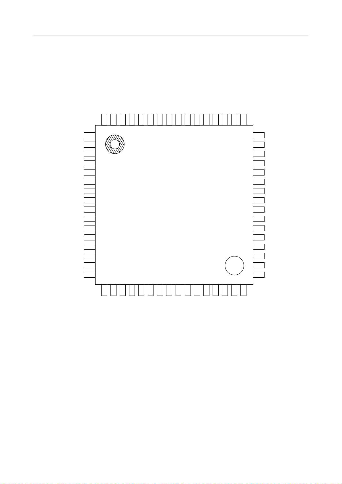
PIN CONFIGURATION (TOP VIEW)
EXCK
DIN
NCTHR
SLPTHR
TEST1
TEST2
TEST3
TEST4
TEST8
PDN/RST
RST
64
63
62
61
60
59
58
57
56
55
54
53 SYNC
52 BCLK
51 CLKSEL
50 PCMI
49 PCMEI
ECSEL
MCUSEL
AHD
AHLD
AATT
AGC
DGND1
ATHR
LHD
LHLD
LATT
DD1
10
11
12LGC
13LTHR
14RPAD4
15DV
16RPAD3
1
2
3
4
5
6
7
8
9
48
PCMEO
47
PCMO
46
PCMSEL
45
SYNCSEL
44
DOUT
43
DEN
42
DV
GLPADTHR
41
TEST9
40
LINEEN
39
AGND
38
DD2
37 LOUT
36 LPWI
35 LVFRO
34 LGSX
33 LIN
17
18
19
20
21
22
23
24
25
26
27
28AIN
29AVFRO
30APWI
31AOUT
32SG
DD
X2
AV
RPAD2
RPAD1
TPAD4
DGND2
TPAD3
TPAD2
TPAD1
MCK/X1
AGSX
64-Pin Plastic QFP
3/43
¡ Semiconductor MSM7731-01
PIN DESCRIPTIONS
Pin PinType TypeSymbol Symbol
133
234
335
AHD
436
537
638
AATT
AGC
739
840
941
LHD GLPADTHR
10 42
11 43
12 44
LATT DEN
LGC
13 45
14 46
15 47
DD1
16 48
17 49
18 50
19 51
20 52
21 53
22 54
23 55
24 56
25 57
26 58
DD
27 59
28 60
29 61
30 62
31 63
32 64
IIECSEL LIN
IOMCUSEL LGSX
IO
LVFRO
IIAHLD LPWI
IO
II
IIDGND1
LOUT
AGND
LINEEN
IOATHR TEST9
II
IILHLD DV
DD2
II
IO
DOUT
IILTHR SYNCSEL
IIRPAD4 PCMSEL
IODV
PCMO
IORPAD3 PCMEO
IIRPAD2 PCMEI
IIRPAD1 PCMI
IIDGND2 CLKSEL
I I/OTPAD4 BCLK
I I/OTPAD3 SYNC
IITPAD2
IITPAD1
RST
PDN/RST
IIMCK/X1 TEST8
OIX2 TEST4
IIAV
TEST3
OIAGSX TEST2
IIAIN TEST1
OIAVFRO SLPTHR
IIAPWI NCTHR
OIAOUT DIN
OISG EXCK
4/43
¡ Semiconductor MSM7731-01
g
PIN FUNCTIONAL DESCRIPTION
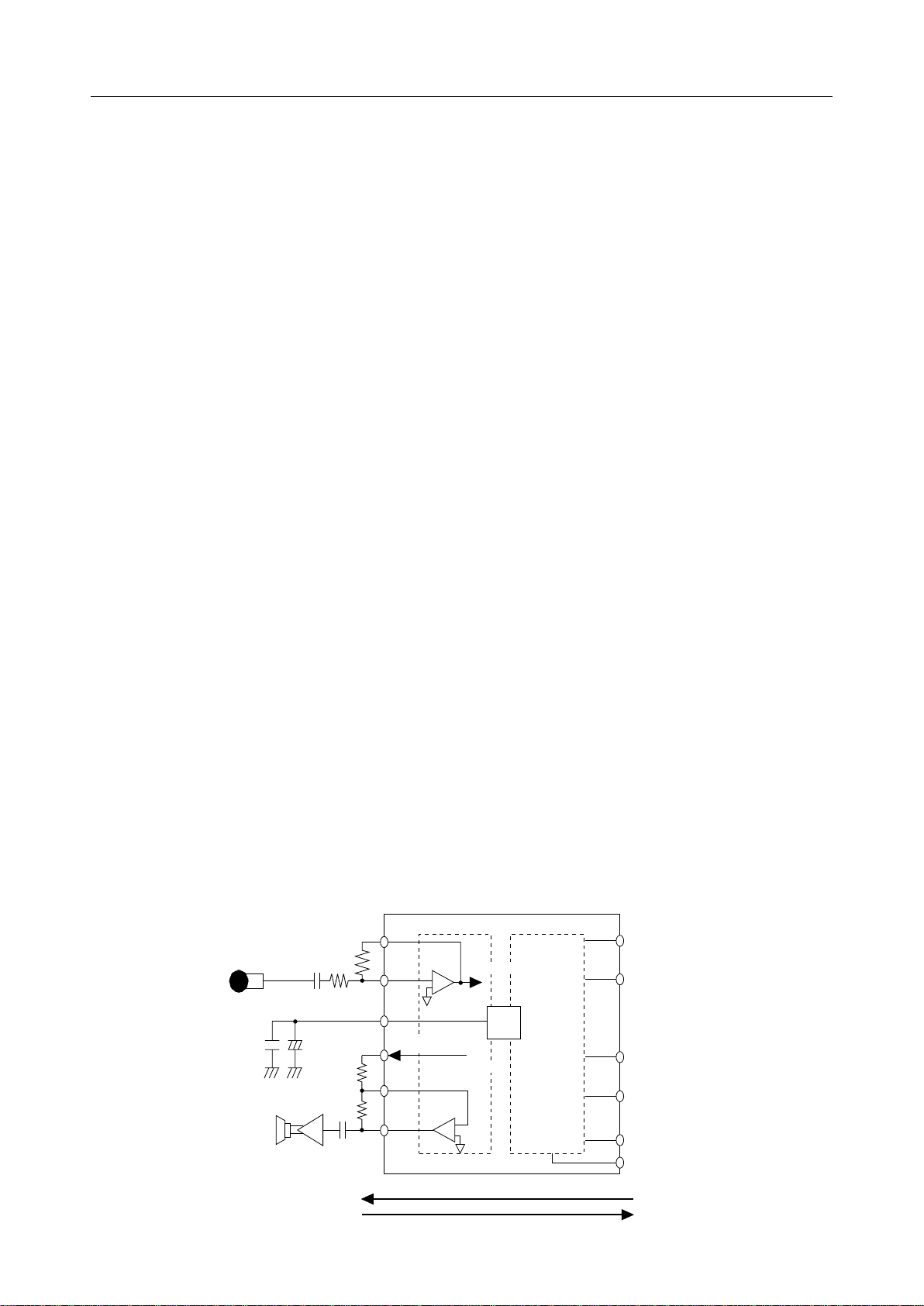
AIN, AGSX
These are the acoustic analog input and level adjusting pins. The AIN pin is connected to the
inverting input of the internal amp and the AGSX pin is connected to the amp output. For level
adjustment, refer to the diagram below (Figure 1). At power-down reset, the AGSX pin goes to
a high impedance state.
AVFRO, AOUT, APWI
These are the acoustic analog output and level adjusting pins. The AVFRO pin is an audio
output and can directly drive 20 kW. The AOUT pin is an analog output and can directly drive
a load of 1.2 kW. For level adjustment, refer to the diagram below (Figure 1). At power-down
reset, these output pins go to a high impedance state.
LIN, LGSX
These are the line analog input and level adjusting pins. The LIN pin is connected to the
inverting input of the internal amp and the LGSX pin is connected to the amp output. For level
adjustment, refer to the diagram below (Figure 1). At power-down reset, the LGSX pin goes to
a high impedance state. If LIN is not used, short the LIN and LGSX pins together.
LVFRO, LOUT, LPWI
These are the line analog output and level adjusting pins. The LVFRO pin is an audio output
and can directly drive 20 kW. The LOUT pin is an analog output and can directly drive a load
of 1.2 kW. For level adjustment, refer to the diagram below (Figure 1). At power-down reset,
these output pins go to a high impedance state. If LOUT is not used, short the LPWI and LOUT
pins together.
LINEEN
This is the power-down control pin for the line CODEC. A logic "0" continues normal operation
and a logic "1" powers down only the line CODEC. If the line CODEC is not used, power down
the line CODEC and short the LIN pin to the LGSX pin and the LPWI pin to the LOUT pin. This
procedure results in the low consumption of electrical power. At power-down, the output pins
go to a high impedance state. Since this pin is ORed with CR0-B5 of the control register, set the
pin to a logic "0" when controlling power-down by the control register. If the pin setting is
changed, reset must be activated by either the PDN/RST pin or the PDN/RST bit (CR0-B7).
=R2/R1
V
AGSX/VI
£30
Speaker
R2≥20kW
V
I
Speaker amp
V
O/VAVFRO
R3≥20kW
+
–
10mF0.1mF
=R3/R4
R1C1
C2
Microphone
Acoustic side (microphone, speaker)
R2
R3
R4
V
O
AGSX
AIN
SG
AVFRO
APWI
AOUT
Acoustic CODEC
to ENCODER
–
+
from DECODER
–
+
Reception signal
Transmission si
VREF
Line CODEC
nal
LGSX
LIN
Same as the acoustic
analog interface
LVFRO
LPWI
LOUT
LINEEN
Line side (portable phone)
Figure 1 Analog Interface
5/43
¡ Semiconductor MSM7731-01
AGND
This is the analog ground pin.
DGND1, DGND2
These are the digital ground pins.
AV
DD
This is the analog +3 V power supply pin.
DV
DD1
, DV
DD2
These are the digital +3 V power supply pins.
SG
This is the output pin for the analog signal ground potential. The output voltage is approximately
1.4 V. Insert 10 mF and 0.1 mF ceramic bypass capacitors between the AGND and SG pins. At
power-down reset, this output becomes 0 V.
PDN/RST
This is the power-down reset control input pin. If a logic "0" is input to this pin, the device enters
the power-down state. At this time, all control register bits and internal variables will be reset.
After the power-down reset state is released, the device enters the initial mode (refer to the CR0
control register description). During normal operation, set this pin to a logic "1". Since the
PDN/RST pin is ORed (negative logic) with CR0-B7 of the control register, set the pin to a logic
"1" when controlling power-down reset by the control register.
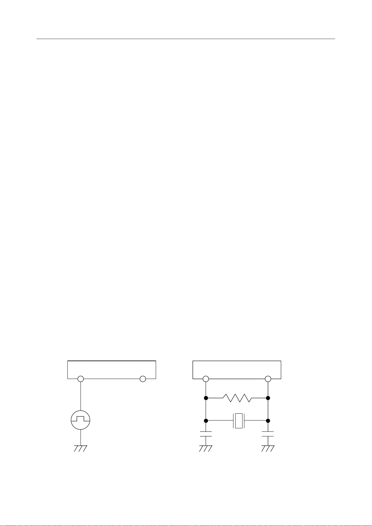
MCK/X1
This is the master clock input pin. The clock frequency is 19.2 MHz. The input clock may be
asynchronous with respect to the SYNC signal or the BCLK signal. Refer to Figure 2 (a) for an
example application of an external clock and Figure 2 (b) for an example oscillator circuit.
X2
This is the crystal oscillator output pin. If an existing external clock is to be used, leave this pin
open and input the clock to the MCK pin. Refer to Figure 2 (b) for an example oscillator circuit.
MCK/X1 X2 MCK/X1 X2
R
Figure 2 (a) External Clock Application
Crystal
CC
R
C
Crystal
Figure 2 (b) Oscillator Circuit Example
: T.B.D
: T.B.D
: 19.2 MHz
Example
6/43

¡ Semiconductor MSM7731-01
SYNC
This is the 8 kHz sync signal I/O pin for digital data communication. This pin is switched to
function as an input or output by the CLKSEL pin. If the internal clock mode is selected by the
CLKSEL pin, an 8 kHz clock synchronized to the BCLK signal is output and digital data
communication is performed. If the external clock mode is selected by the CLKSEL pin, this pin
becomes an input that requires an 8 kHz clock input synchronized to the BCLK pin, and digital
data communication is performed based on this input clock. Fixing this signal to a logic "1" or
logic "0" causes this device to internally write a logic "1" to the PDN/RST (CR0-B7) bit of the
control register, and to enter the power-down reset state. This automatic power-down control
is valid when external clock mode is selected by the CLKSEL pin and automatic power-down
control has been turned ON by the SYPDN (CR11-B0) bit of the control register.
BCLK
This is the shift clock I/O pin for digital data communication. This pin is switched to function
as an input or output by the CLKSEL pin. If the internal clock mode is selected by the CLKSEL
pin, a 64 kHz or 128 kHz clock synchronized to the SYNC signal is output and digital data
communication is performed. Switching between 64 kHz and 128 kHz is performed by the
PCMSEL pin. If m-law PCM is selected by the PCMSEL pin, a 64 kHz clock is output. Or, if 16bit linear mode is selected, a 128 kHz clock is output. If the external clock mode is selected by
the CLKSEL pin, this pin becomes an input that requires a clock input synchronized to the
SYNC. In this case, the clock frequency range is from 64 kHz to 2048 kHz.
CLKSEL
This pin selects internal or external clock modes for the SYNC and BCLK signals. A logic "0"
selects the internal clock mode. At this time, SYNC and BCLK pins are configured as output pins
and each internally generated clock is output to perform digital data communication. A logic
"1" selects the external clock mode and configures the SYNC and BCLK pins as input pins. At
this time, digital data communication is performed with the externally input SYNC and BCLK
clocks. If digital data communication is not used, set this pin to a logic "0" to select internal
clocks. If the pin setting is changed, reset must be activated by either the PDN/RST pin or the
PDN/RST bit (CR0-B7).
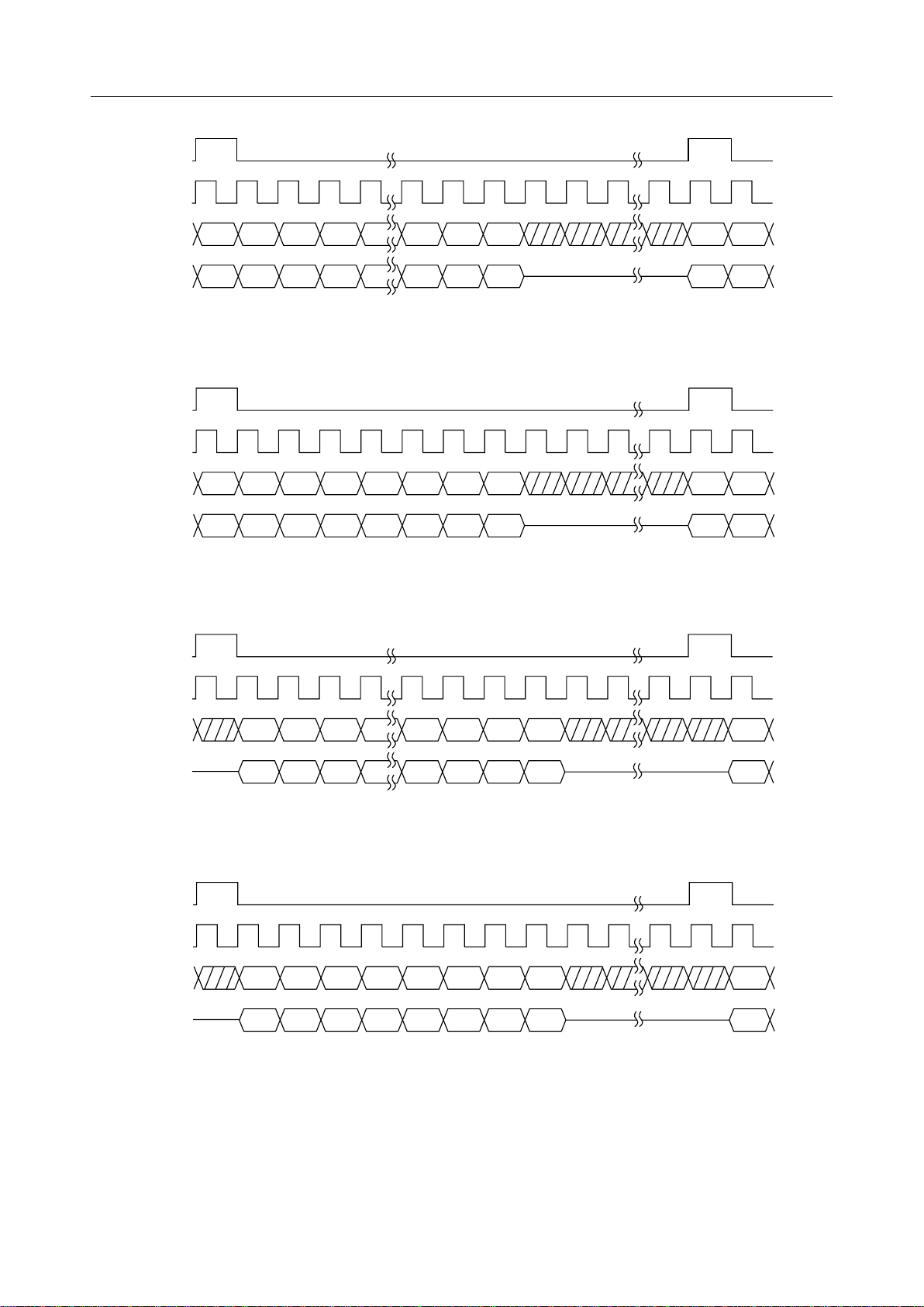
PCMI
This is the digital receive signal input pin on the line-side. This input signal is shifted at the
rising edge of the BCLK signal and input. The beginning of digital data is identified on the rising
edge of the SYNC signal. The coding format can be selected as m-law PCM or 16-bit linear (2's
complement) by the PCMSEL pin. If the PCMI pin is not used, set it to a logic "1" if m-law PCM
has been selected, or a logic "0" if 16-bit linear mode has been selected. The sync format can be
selected as normal-sync or short-frame-sync by the SYNCSEL pin. Refer to Figure 3 for the
timing. This digital input signal is added internally to the CODEC digital output signal. Be
careful of overflow when using the CODEC.
PCMO
This is the digital transmit signal output pin on the line-side. This output signal is synchronized
to the rising edge of the BCLK and SYNC signals and then output. When not used for output,
this pin is in the high impedance state. It is also at high impedance during the power-down reset
and the initial modes. The coding format can be selected as m-law PCM or 16-bit linear (2's
complement) by the PCMSEL pin. The sync format can be selected as normal-sync or shortframe-sync by the SYNCSEL pin. Refer to Figure 3 for the timing.
7/43

¡ Semiconductor MSM7731-01
PCMEI
This is the message signal input pin. Use this pin when a message is output to the speaker on
the acoustic-side. This input signal is shifted at the rising edge of the BCLK signal and then
input. The beginning of digital data is identified on the rising edge of the SYNC signal. The
coding format can be selected as m-law PCM or 16-bit linear (2's complement) by the PCMSEL
pin. If the PCMEI pin is not used, set it to a logic "1" if m-law PCM has been selected, or a logic
"0" if 16-bit linear mode has been selected. The sync format can be selected as normal-sync or
short-frame sync by the SYNCSEL pin. Timing is the same as for the PCMI pin (refer to Figure
3). This digital input signal is added internally to the echo canceler output signal. Be careful
of overflow during telephone conversations.
PCMEO
This output pin is for memo recording. Use it with the memo function. This output signal is
synchronized to the rising edge of the BCLK and SYNC signals and then output. When not used
for output, this pin is in the high impedance state. It is also at high impedance during the powerdown reset and the initial modes. The coding format can be selected as m-law PCM or 16-bit
linear (2's complement) by the PCMSEL pin. The sync format can be selected as normal-sync
or short-frame-sync by the SYNCSEL pin. Timing is the same as for the PCMO pin (refer to
Figure 3).
SYNCSEL
This is the sync timing selection pin for digital data communication. A logic "0" selects
normal-sync timing and a logic "1" selects short-frame-sync timing. Refer to Figure 3 for the
timing. If the pin setting is changed, reset must be activated by either the PDN/RST pin or the
PDN/RST bit (CR0-B7).
PCMSEL
This is the coding format selection pin for digital data communication. A logic "1" selects m-law
PCM and a logic "0" selects 16-bit linear (2's complement) coding format. When an internal clock
is selected, the BCLK signal determines the output clock frequency. If the digital interface is not
used, set this pin to logic "0" to select 16-bit linear coding format.
Since this pin is logically ORed with the PCMSEL bit (CR11-B1), set the pin to a logic "0" when
controlling by the control register.
If the pin setting is changed, reset must be performed by either the PDN/RST pin or the PDN/
RST bit (CR0-B7).
8/43
¡ Semiconductor MSM7731-01
SYNC
BCLK
PCMI
PCMEI
PCMO
PCMEO
SYNC
BCLK
PCMI
PCMEI
PCMO
PCMEO
SYNC
D15 D14 D13 D12 D2 D1 D0 D15 D14
D15 D14 D13 D12 D2 D1 D0 D15 D14
Hi-Z
(a) 16-bit linear coding format timing (normal sync)
D7 D6 D5 D4 D2 D1 D0 D7 D6
D7 D6 D5 D4D3D3 D2 D1 D0 D7 D6
mm
(b)
m-law PCM coding format timing (normal sync)
mm
Hi-Z
BCLK
PCMI
PCMEI
PCMO
PCMEO
SYNC
BCLK
PCMI
PCMEI
PCMO
PCMEO
D15 D14 D13 D2 D1 D0 D15
D15 D14 D13
D3
D3 D2 D1 D0 D15
Hi-ZHi-Z
(c) 16-bit linear coding format timing (short-frame sync)
D7 D6 D5 D4 D2 D1 D0 D7
D7 D6 D5 D4D3D3 D2 D1 D0 D7
mm
(c)
m-law PCM coding format timing (short-frame sync)
mm
Hi-ZHi-Z
Figure 3 Digital Interface Timing
9/43

¡ Semiconductor MSM7731-01
ECSEL
This is the echo canceler mode selection pin. A logic "1" selects the single echo canceler mode
and a logic "0" selects the dual echo canceler mode. Since this pin is ORed with the CR0-B0 bit
of the control register, set the pin to a logic "0" when controlling by the control register. If the
pin setting is changed, reset must be activated by either the PDN/RST pin or the PDN/RST bit
(CR0-B7). If the single echo canceler mode is selected, echo canceler control on the line-side is
unnecessary.
LTHR/ATHR
This is the "through mode" control pin for the echo canceler. In the "through mode", SinL/A and
RinL/A data is directly output to SoutL/A and RoutL/A respectively while each respective
echo coefficient is maintained. A logic "0" selects the normal mode (echo canceler operation) and
a logic "1" selects the "through mode." Since this pin is ORed with the CR4-B7 and CR5-B7 bits
of the control register, set the pin to a logic "0" when controlling the "through mode" by the
control register. Because data is shifted into this pin in synchronization with the rising edge of
the SYNC signal, hold the data at the pin for 250 ms or longer. For further details, refer to the
electrical characteristics.
LHD/AHD
This pin turns ON or OFF the function to detect and cancel the howling that occurs in an acoustic
system such as a handsfree communication system. A logic "0" turns the function ON and a logic
"1" turns the function OFF. Since this pin is ORed with the CR4-B4 and CR5-B4 bits of the control
register, set the pin to a logic "0" when controlling by the control register. Because data is shifted
into this pin in synchronization with the rising edge of the SYNC signal, hold the data at the pin
for 250 ms or longer. For further details, refer to the electrical characteristics.
LHLD/AHLD
This pin controls the updating of adaptive FIR filter coefficients for the echo canceler. A logic
"0" selects the normal mode (coefficient updating) and a logic "1" selects the fixed coefficient
mode. Since this pin is ORed with the CR4-B2 and CR5-B2 bits of the control register, set the pin
to a logic "0" when controlling by the control registers. Because data is shifted into this pin in
synchronization with the rising edge of the SYNC signal, hold the data at the pin for 250 ms or
longer. For further details, refer to the electrical characteristics.
LATT/AATT
This pin turns ON or OFF the ATT function to prevent howling by means of attenuators
(ATTsL/A, ATTrL/A) provided in the RinL/A inputs and SoutL/A outputs of the echo
canceler. If input is only to RinL/A, the ATTsL/A for SoutL/A is activated. If input is only to
SinL/A, or if there is input to both SinL/A and RinL/A, the ATTrL/A for RinL/A input is
activated. The ATT value of each attenuator is approximately 6 dB. A logic "0" turns ON and
a logic "1" turns OFF the ATT function. Since this pin setting is logically ORed with the CR4B1 and CR5-B1 bits of the control register, set the pin to a logic "0" when controlling by the control
register. Because data is shifted into this pin in synchronization with the rising edge of the SYNC
signal, hold the data at the pin for 250 ms or longer. For further details, refer to the electrical
characteristics.
10/43

¡ Semiconductor MSM7731-01
LGC/AGC
This pin turns ON or OFF the gain control function to control the input level and prevent
howling by means of gain controls (GainL/A) provided in the RinL/A inputs of the echo
canceler. The gain controller adjusts the RIN input level when it is –10 dBm0 or above, and it
has the control range of 0 to –8.5 dB. A logic "0" turns the function ON and a logic "1" turns the
function OFF. Since this pin is ORed with the CR4-B0 and CR5-B0 bits of the control register,
set the pin to a logic "0" when controlling by the control register. Because data is shifted into this
pin in synchronization with the rising edge of the SYNC signal, hold the data at the pin for 250
ms or longer. For further details, refer to the electrical characteristics.
Notes:
Lxx/Axx: In the above, Lxx refers to line echo canceler control pins and Axx to acoustic echo
canceler control pins.
xxL/xxA: In the above pin descriptions, xxL refers to line echo canceler functions and xxA to
acoustic echo canceler functions.
GLPADTHR
This is the mode control pin for the attenuators (LPADL/A) provided in the SinL/A inputs and
the amplifiers (GPADL/A) provided in the SoutL/A outputs of the echo canceler. A logic "0"
selects the "through mode" and a logic "1" selects the normal mode (PAD operation). The levels
are set by the CR10 register. Settings of ±18, ±12, ±6 and 0 dB are possible. The default setting
is ±12 dB. If the echo return loss (value of returned echo) is amplified, set the LPAD level such
that echo return loss will be attenuated. It is recommended to set the GPAD level to the positive
level equal to the LPAD level. Since this pin is ORed with the CR1-B2 bit of the control register,
set the pin to a logic "0" when controlling by the control register. Because data is shifted into this
pin in synchronization with the rising edge of the SYNC signal, hold the data at the pin for 250
ms or longer. For further details, refer to the electrical characteristics.
NCTHR
This is the noise canceler "through mode" control pin. In the "through mode" the noise canceler
is halted and data is directly output. A logic "0" selects the normal mode (noise canceler
operation) and a logic "1" selects the "through mode". Since this pin is ORed with the CR1-B0
bit of the control register, set the pin to a logic "0" when controlling by the control register.
Because data is shifted into this pin in synchronization with the rising edge of the SYNC signal,
hold the data at the pin for 250 ms or longer. For further details, refer to the electrical
characteristics. When this pin is changed from normal mode to "through mode", approximately
20 ms of data dropout will occur.
SLPTHR
This is the "through mode" control pin for the transmit slope filter. In the "through mode", the
filter is halted and data is directly output. A logic "0" selects the normal mode (slope filter
operation) and a logic "1" selects the "through mode". Since this pin is ORed with the CR1-B1
bit of the control register, set the pin to a logic "0" when controlling by the control register.
Because data is shifted into this pin in synchronization with the rising edge of the SYNC signal,
hold the data at the pin for 250 ms or longer. For further details, refer to the electrical
characteristics.
11/43

¡ Semiconductor MSM7731-01
RST
This input pin resets coefficients of the echo canceler and noise canceler. A logic "0" causes the
reset state to be entered. At this time, the filter coefficients for the echo canceler and noise
canceler are reset. Control register contents are preserved. While reset is being processed, there
is no sound. During normal operation, set this pin to a logic "1". Since this pin is ORed (negative
logic) with the CR0-B6 bit of the control register, set the pin to a logic "1" when controlling by
the control register. Use this pin in cases where the echo path changes (due to line switching
during a telephone conversation, etc.), or when resuming telephone communication. Because
data is shifted into this pin in synchronization with the rising edge of the SYNC signal, hold the
data at the pin for 250 ms or longer.
For further details, refer to the electrical characteristics.
DEN, EXCK, DIN, DOUT
This is the serial port for the microcomputer interface. 13 bytes of control registers are provided
in this LSI device. These pins are used to write and read data from an external microcomputer.
The DEN pin is an enable signal input pin, the EXCK pin is a clock signal input pin for data
shifting, the DIN pin is an address and data input pin, and the DOUT pin is a data output pin.
If the microcomputer interface is not used, set the DEN pin to a logic "1" and the EXCK and DIN
pins to a logic "0". In addition, use the MCUSEL pin to specify the "unused" setting of the
microcomputer interface. Figure 4 shows the input timing.
MCUSEL
This pin selects whether the microcomputer interface is used or unused. A logic "0" specifies
that the microcomputer interface is used and a logic "1" specifies that it is not used. If the
microcomputer interface is not used, this pin must be set to a logic "1". This pin is ORed with
the CR0-B1 bit of the control register.
12/43
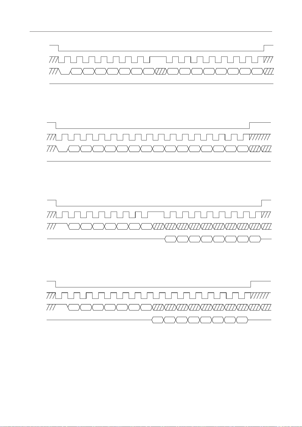
¡ Semiconductor MSM7731-01
DEN
1
EXCK
2 3 4 5 6 7 8 9 10 11 12 13 14 15 16
DIN
DOUT
DEN
EXCK
DIN
DOUT
DEN
EXCK
A6W A5A4A3A2A1A0 B7B6B5B4B3B2B1B0
Hi-Z
(a) Data Write Timing 1 (8-Bit MCU)
1
2 3 4 5 6 7 8 10 11 12 13 14 15 16
A6W A5A4A3A2A1A0B7B6B5B4B3B2B1B0
9
Hi-Z
(b) Data Write Timing 2 (16-Bit MCU)
1
2 3 4 5 6 7 8 9 10 11 12 13 14 15 16
DIN
DOUT
DEN
EXCK
DIN
DOUT
A6R A5A4A3A2A1A0
Hi-Z Hi-Z
B6B7 B5 B4 B3 B2 B1 B0
(c) Data Read Timing 1 (8-Bit MCU)
1
2 3 4 5 6 7 8 9 10 11 12 13 14 15 16
A6R A5A4A3A2A1A0
Hi-Z Hi-Z
B6B7 B5 B4 B3 B2 B1 B0
(d) Data Read Timing 2 (16-Bit MCU)
Figure 4 Microcomputer Interface I/O Timing
13/43
 Loading...