

OKI MSM7728GS-K Datasheet

E2U0053-28-81
¡ Semiconductor MSM7728
¡ Semiconductor
This version: Aug. 1998
Previous version: Apr. 1997
MSM7728
Single Rail Linear CODEC
GENERAL DESCRIPTION
The MSM7728 is a single-channel linear CODEC CMOS IC for voice signals that contains filters
for A/D and D/A conversions.
Designed especially for a single-power supply and low-power applications, the device is
optimized for applications for the analog interfaces of audio signal processing DSPs and digital
wireless systems.
The analog outputs include the speaker drive output, earphone drive output and ringer output.
Therefore, the sound interface can be configured with a few external circuits.
FEATURES
• Single power supply : 2.5 V to 3.6 V
• Low power consumption
Operating mode : 36 mW Typ.
Power down mode : 0.003 mW Typ.
• Digital signal input/output interface : 14-bit serial code in 2's complement format
• Transmission clock frequency : 112 kHz min., 2048 kHz max.
• Filter characteristics : Complies with ITU-T Recommendation G.714
• Built-in PLL eliminates a master clock
• Built-in PB tone signal generator
• Built-in service tone generator
• Built-in ringer tone generator
• General latch output: 1 bit
• Both transmit and receive gain adjustable by external control
• Receive interface: Speaker direct drive output
Earphone interface output : 600 W, 1 mW max.
Ringer output : 70 nF, 4 V
• Transmit gain adjustable using an external resistor
• Transmit microphone amplifier is eliminated by the gain setting of a maximum of 36 dB.
• Built-in reference voltage supply
• Serial 8-bit processor interface
• Package:
30-pin plastic SSOP (SSOP30-P-56-0.65-K) (Product name: MSM7728GS-K)
PP
1/23
¡ Semiconductor MSM7728
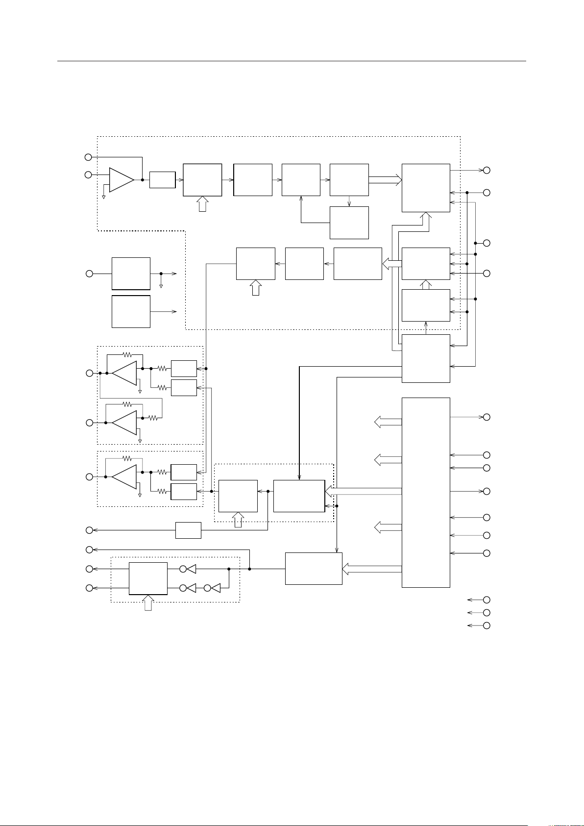
BLOCK DIAGRAM
MAO
MAIN
SGC
SPKP
SPKN
CODEC
–
+
GEN
GEN
SW1
SG
VR
SPK
–
+
–
+
VOL1
SW 2
SW 4
RC
LPF
VOL2
8th
BPF
5th
LPF
14 BIT
ADCONV
AUTO
ZERO
14 BIT
DACONV
SW CONTROL
TCONT
RCONT
RTIM
PLL
PCMOUT
SYNC
BCLK
PCMIN
LA
EAR
TOUT
LED
RINGP
RINGN
EAR
–
+
VOL4
SW 3
SW 5
SW 6
Tone GEN
VOL3
PB Tone
SERVICE Tone
RINGER
Tone
VOL CONTROL
POWER-DOWN
CONTROL
MCU
INF.
WRN
RDN
CDOUT
CDIN
DCLK
RSTN
V
DD
AG
DG
2/23

¡ Semiconductor MSM7728
PIN CONFIGURATION (TOP VIEW)
SPKP
SPKN
EAR
RINGP
RINGN
TOUT
LED
LA
NC
RDN
CDOUT
WRN
DCLK
CDIN
DG
1
2
3
4
5
6
7
8
9
10
11
12
13
14
15
NC: No connection
30
29
28
27
26
25
24
23
22
21
20
19
18
17
16
AG
NC
NC
SGC
MAO
MAIN
NC
V
DD
NC
NC
RSTN
SYNC
BCLK
PCMOUT
PCMIN
30-Pin Plastic SSOP
3/23
¡ Semiconductor MSM7728
PIN AND FUNCTIONAL DESCRIPTIONS
V
DD
Power supply pin for 2.5 to 3.6 V (Typically 3.0 V).
AG
Analog signal ground.
DG
Ground pin for the digital signal circuits.
This ground is separated from the analog signal ground in this device. The DG pin must be
connected to the AG pin on the printed circuit board.
SGC
Bypass capacitor pin for generating the signal ground voltage level.
Insert a 0.1 mF capacitor with excellent high frequency characteristics between the AG pin and
the SGC pin.
MAIN, MAO
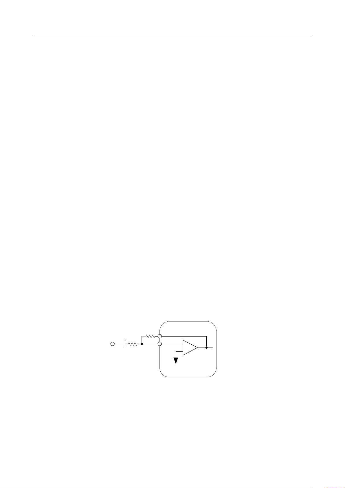
Transmit microphone input and level adjustment.
MAIN is connected to the inverting input of the op-amp, and MAO is connected to the output
of the op-amp. This amplifier can set up a gain to a maximum of 36dB by using an external
resistor.
Level adjustment should be performed in a way below.
A transmit level of +6, 0, –6, or –12dB can be selected using control data from the processor
interface.
When CODEC is turned off, the MAO output goes high impedance.
R1 : variable
R2 > 20 kW
C1 > 1/(2 ¥ 3.14 ¥ 30 ¥ R1) (F)
Gain = R2/R1 < 63
Microphone input
C1
R1
R2
MAO
MAIN
–
+
SG
4/23

¡ Semiconductor MSM7728
SPKP, SPKN
These pins are used for speaker driving.
The SPKN output is reversed in phase against the SPKP output when the gain is 1.
The receive output signal amplitude is 2.2VPP at maximum.
These outputs swing around the SG potential (signal ground potential, VDD/2) and can drive the
minimum 0.6kW load in pushpull driving mode.
The maximum output amplitude is 4.4VPP in pushpull driving mode (a load is inserted between
SPKN and SPKP).
Control data from the processor interface allows selecting the D/A conversion output, PB tone
output, or service tone output and also can provide a level control and mute control. When SPK
is turned off, the SG potential is output with high resistance.
EAR
Analog output for external accessary circuit.
This output swings around the SG potential and can drive the minimum 0.6kW against the SG
potential.
Control data from the processor interface allows selecting the D/A conversion output, PB tone
output, or service tone output and also can provide a level control and mute control. When EAR
is turned off, the SG potential is output with high resistance.
BCLK
Shift clock signal input for PCMIN and PCMOUT.
The frequency is equal to the data signaling rate.
SYNC
Synchronizing signal input.
In the transmit section, the PCM output signal from the PCMOUT pin is output synchronously
with this synchronizing signal. This synchronizing signal triggers the PLL and synchronizes all
timing signals of the transmit section.
In the receive section, 14 bits required are selected from serial input of PCM signals on the PCMIN
pin by the synchronizing signal.
Signals in the receive section are synchronized by this synchronizing signal. This signal must be
synchronized in phase with the BCLK.
When this signal frequency is 8 kHz, the transmit and receive paths have the frequency
characteristics specified by ITU-T G. 714. The frequency characteristics for 8 kHz are specified in
this data sheet.
For different frequencies of the SYNC signal, the frequency values in this data sheet should be
translated according to the following equation:
Frequency values described in the data sheet
8 kHz
¥ the SYNC frequency values to be actually used
5/23
¡ Semiconductor MSM7728
PCMIN
PCM signal input.
A serial PCM signal input to this pin is converted to an analog signal synchronously with the
SYNC signal and BCLK signal.
The data signaling rate of the PCM signal is equal to the frequency of the BCLK signal.
The PCM signal is shifted at the falling edge of the BCLK signal. The PCM signal is latched into
an internal register when shifted by 14 bits.
The top of the data (MSD) is identified at the rising edge of SYNC.
The input signal should be input in the 14-bit 2's complement format.
The MSD bit represents the polarity of the signal with respect to the signal ground.
PCMOUT
PCM signal output.
The PCM output signal is output starting with MSD in sequential order, synchronously with the
rising edge of the BCLK signal.
MSD may be output at the rising edge of the SYNC signal, depending on the timing between
BCLK and SYNC.
This pin is in a high impedance state except during 14-bit PCM output. It is also high impedance
when the CODEC is turned off.
A pull-up resistor must be connected to this pin, because its output is configured as an open
drain.
The output coding format is in 14-bit 2's complement.
The MSD represents a polarity of the signal with respect to the signal ground.
Input/Output Level
+Full scale
+1
0
–1 1111 1111 1111 11
–Full scale
Table 1
PCMIN/PCMOUT
MSD
0111 1111 1111 11
0000 0000 0000 01
0000 0000 0000 00
1000 0000 0000 00
6/23

¡ Semiconductor MSM7728
WRN, RDN, DCLK, CDIN, CDOUT
Serial control ports for microcontroller interface.
Writing data to 8-bit control registers allows controling the transmit speech path/receive speech
path mute, transmit speech path/receive speech path level, PB tone, service tone, and ringer.
WRN is the write control signal input, RDN is the read control signal input, DCLK is the clock
signal input for data shift, CDIN is the control data input, CDOUT is the control data output.
When reset (RSTN=0), the control registers are reset to the initial values as described in "Control
Data Description".
The initial values remains unchanged until control data is written after reset.
Writing of control data: When WRN is at digital "0", data that is entered in CDIN is shifted at the
rising edge of the DCLK signal pulse and is latched in an internal control register.
Reading of control data: When RDN is at digital "0", control data is output from CDOUT at the
rising edge of a DCLK signal pulse.
See Figure 2 for write and read timings.
RINGP, RINGN
Ringer (sounder) drive outputs.
The sounder can be structured by putting a piezo-electric type sounding body (equivalent
capacitance: less than 70nF) between RINGP and RINGN.
LED
Ringer digital level output. This pin is used for LED blinking synchronous with the ringer.
LA
General latch output. This output is used as a control signal for a peripheral circuit because this
output can be set to digital "0" or "1" by writing data from a microcontroller interface.
TOUT
PB tone/service tone output. When SW6 is in the ON state, tone is output.
The output resistance of this pin is approximately 10kW, which should be taken into account
when using it externally.
RSTN
Control register reset signal input. When this pin is set to digital "0" level.
All control registers are reset to the initial values.
Be sure to reset the control registers after turning on the power.
7/23
 Loading...