E2A0030-16-X1
¡ Semiconductor MSM7715
¡ Semiconductor
This version: Jan. 1998
Previous version: Nov. 1996
MSM7715
Multi-Function Telecommunication LSI
GENERAL DESCRIPTION
The MSM7715 is a signal transmitting and receiving LSI device for applications such as
telemeters. The MSM7715 uses a no-ringing communication mode. Built-in functions includes
a 300 bps full-duplex modem complying with ITU-T V.21, a DTMF signal (PB signal) generator
and receiver, and a call progress tone (CPT) detector. The answer tone (1650 Hz) generation can
be accomplished with the built-in modem.
A meter terminal can be configured using this transmitting and receiving device along with the
meter, NCU, and controller.
FEATURES
• 3 V power supply. (Voltage range is 2.5 V to 3.6 V.)
• Selectable modes, including DTMF signal sending mode, DTMF signal receiving mode, and
V.21 modem answer/originate mode.
• For DTMF signal reception, support for normal detection mode or high-speed detection mode.
• For call progress tone detection, support for rectangular wave output or detection output.
• DTMF signal receiving output, which is in a 3-state mode, is able to be connected externally
with the DTMF signal sending 4-bit input.
• Analog loopback test and remote digital loopback test supported.
• Dedicated pins for modem sending/receiving data, carrier detection, sending request, and call
progress tone detection.
• Independent external adjustment of the analog signal using the modem signal and DTMF
signal.
• External adjustment of the carrier detection level.
• Internal 3.579545 MHz crystal oscillation circuit.
• Power-down mode
• Package:
44-pin plastic QFP (QFP44-P-910-0.80-2K) (Product name : MSM7715GS-2K)
1/21

¡ Semiconductor MSM7715
2/21
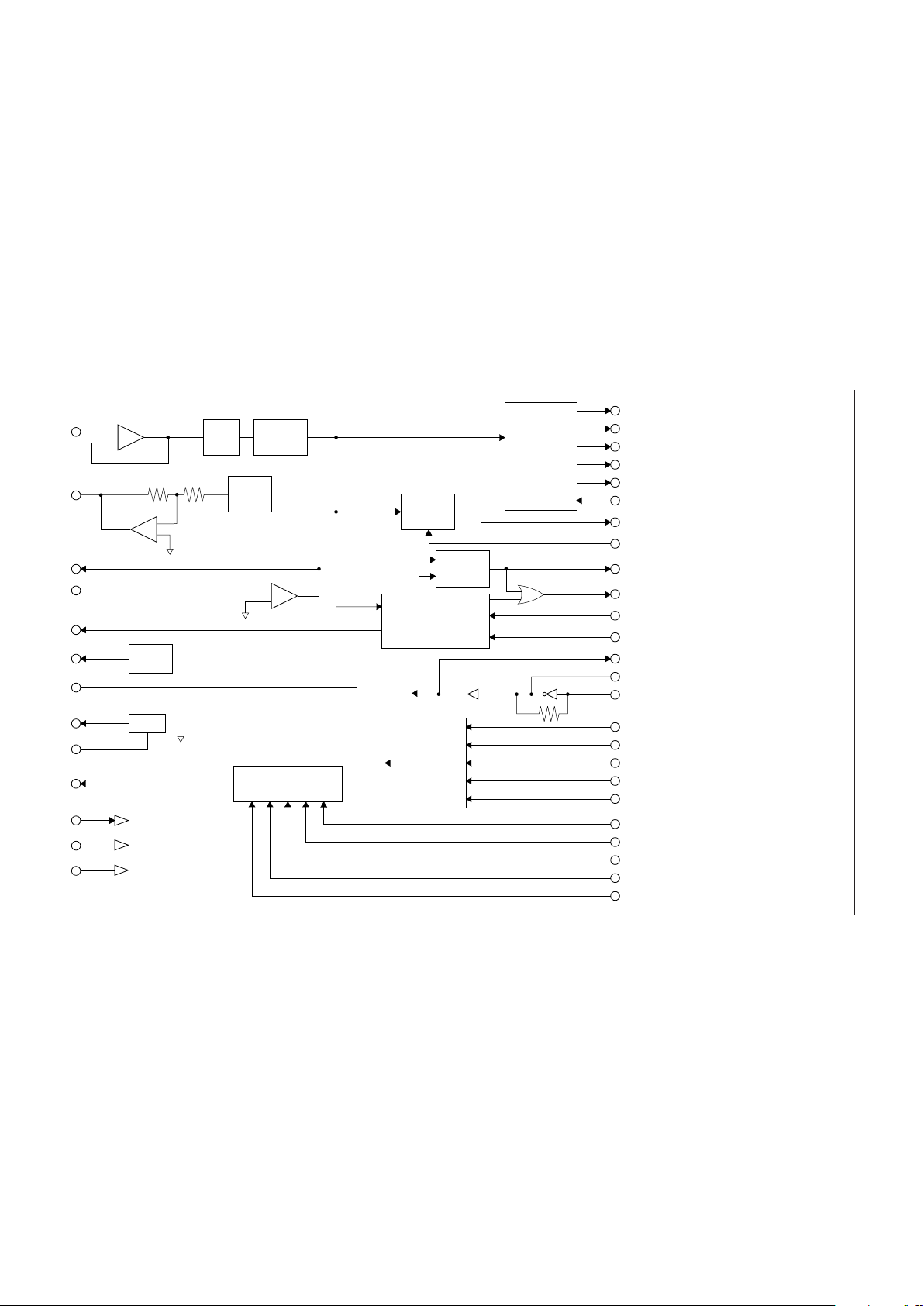
BLOCK DIAGRAM
DT1
DT2
DT3
DT4
SP
DTTIM
CP
CPW
CD
RD
TD
RS
CLK
X2
X1
MODE1
MODE2
MODE3
ICTA
ICTB
TEN
DTG1
DTG2
DTG3
DTG4
AIN
AOUT
GAT2
GAT1
MOD
VR1
VR2
SGO
SGC
DTO
PON
V
DD
GND
Mode
Select
&
Test
FSK Modem
Carrier
Detector
CPT
Detector
DTMF
Receiver
2765 Hz
BEF
PreLPF
Smooth
Voltage
Ref.
SG
DTMF
Generator
+
–
–
+
–
+
*
*
*
*
*
*
*
*
*
*
*
*
*
Power ON
+3 V
0 V
4 dB
Note)
DT1 to DT4 :
3-state outputs
* :
Input with
pull-up resistor
*
*

¡ Semiconductor MSM7715
PIN CONFIGURATION (TOP VIEW)
DTG343DTG242DTG141GND40VR239VR138DTO37MOD36GAT235GAT134SGC
44
DTG4
TEN
TD
RS
CPW
ICTA
ICTB
DTTIM
MODE1
MODE2
MODE3
10
11
1
2
3
4
5
6
7
8
9
12
13X214NC15
X1
16RD17CD18CP19
CLK
DT120DT221DT322DT4
33
32
31
30
29
28
27
26
25
24
23
NC
SGO
AIN
NC
V
DD
NC
AOUT
NC
NC
PON
SP
NC : No connect pin
44-Pin Plastic QFP
3/21

¡ Semiconductor MSM7715
PIN DESCRIPTION
Pin No. I/OName
DTG4
TEN 2
TD 3
RS 4
CPW 5
ICTA 6
ICTB 7
DTTIM 8
MODE1 9
MODE2 10
MODE3 11
X1 12
X2 13
CLK 15
Description
1
I*
Input for specifying the DTMF code to be sent.
Input for controlling output of the DTMF signal. (Transmit enable)
I*
DTG1 to DTG4 are latched at the falling edge of TEN and the DTMF signal is
output when “0” is input. See Fig. 2.
Input for data to be sent to the modem. Input the data string at a speed of 300 bps
I*
or lower.
Input for controlling the modem sending output. (Request to send)
I*
The sending signal is output when “0” is input.
Input for selecting the output waveform from the call progress tone detector.
When "1" is input, a rectangular wave that is synchronized with the input signal is
I*
output from the CP.
When "0" is input, presence of detected signal is output from the CP pin. See Fig.3.
Inputs for testing. Leave them open or connect them to V
I*
Input pin for controlling the detection timing of the DTMF receiver.
I*
When “0” is input, the high-speed detection mode is selected.
I*
Input for selecting the operation mode. See Table 1.
I
Input and output connected to the crystal oscillator. See “Oscillation Circuit” in
the Functional Description.
O
3.579545 MHz clock output
O
DD
.
RD 16
CD 17
CP 18
DT1 19
DT2 20
DT3 21
DT4 22
SP 23
PON 24
AOUT 27
Output for serial data received by the modem. It is held in the marked state
O
(“1”) when the carrier detector (CD) does not make detection.
Output for the carrier detector. “0” means detection, while “1” means
O
non-detection.
Output for call progress tone (CPT) detection. When the CPT is detected,
O
the waveform selected by the CPW pin is output. See Fig. 3.
Outputs for the code of the received DTMF signal. In a mode other than the
O
DTMF receiving mode, these pins are in a high-impedance state.
Output for presenting the DTMF signal receiving data. “1” means that the DTMF
O
signal is being received. Latch DT1 to DT4 at the rising edge of SP.
See Fig. 1.
Input for controlling power-on. When “1” is input, all lines of this device enter the
I*
power down state, and then the operation of each funciton stops and the receiver
timer is reset.
Analog signal output. The DTMF signal or modem sending signal is output.
O
4/21

¡ Semiconductor MSM7715
Pin No. I/OName
V
DD
29
—
AIN 31 I
SGO 32 O
SGC 34
—
GAT1 35 I
GAT2 36 O
MOD 37 O
DTO 38 O
VR1 39 O
VR2 40 I
GND 41
—
DTG1 42
DTG2 43
DTG3 44
Description
Power supply. Supply +2.5V to 3.6V.
Input for the analog receiving signal.
Output for the signal ground voltage. The output voltage is 1/2 V
Connect a capacitor of 0.1 mF or more between SGO and GND.
Pin for connecting the capacitor of the signal ground voltage generating circuit.
Connect a capacitor of 1 mF or more between SGC and GND.
Input for the sending output level-adjusting amplifier.
Output for the sending output level-adjusting amplifier.
Output for the sending modem signal.
Output for the DTMF signal.
Output for the reference voltage generating circuit.
The potential difference between VR1 and SGO is approximately +0.75 V.
Input for external adjustment of the modem’s carrier detection level.
Ground.
Inputs for specifying the DTMF code to be sent.
I*
Data is latched at the falling edge of TEN.
DD
.
Note: Digital inputs that are pulled up internally by a high resistance.
5/21

¡ Semiconductor MSM7715
ABSOLUTE MAXIMUM RATINGS
Parameter Condition UnitRating
Power Supply Voltage
Input Voltage
Storage Temperature
Symbol
V
DD
V
I
T
STG
Ta = 25°C
With respect to GND
—
RECOMMENDED OPERATING CONDITIONS
Parameter Min. Unit
Power Supply Voltage
Operating Temperature Range
Input Voltage
Input Clock Frequency
X1/X2 Load Capacitance
SGC Bypass Capacitance
SGO Bypass Capacitance
V
Bypass Capacitance
DD
Oscillation Frequency
Frequency Deviation
Temperature
Characteristics
V
DD
T
op
V
IH
V
IL
f
CLK
C1, C2
C3
C6
C5
—
—
—
Crystal
Equivalent Series
Resistance
—
ConditionSymbol Typ. Max.
—
—
—
Against 3.579545 MHz
—
—
— 0.1 — —
—
—
At 25°C ±5°C
At –40°C to +85°C
—
–0.3 to 7
–0.3 to VDD + 0.3
–65 to +150
2.5
3.0
–40
0.8 V
DD
0
–0.1
—
—
10
—
3.579545
–100
–50
—
—
—
—
—
12
—
—
—
—
V
V
°C
3.6
+85
V
DD
0.2 V
+0.1
—
1
—
V
°C
V
DD
%
pF
mF
—
MHz
—
+100
ppm
+50
90
W
Load Capacitance
—
—
—
16
—
pF
ELECTRICAL CHARACTERISTICS
DC Characteristics
= 2.5 V to 3.6 V, Ta = –40°C to +85°C)
(V
DD
Parameter Min. Unit
I
Power Supply Current
Input Current
*1
Output Voltage
*2
I
I
V
V
V
V
DD1
DD2
DDS
I
IH
I
IL
OH1
OL1
OH2
OL2
PON = "0"
V
= V
IH
DD
VIL = 0 V
CLK
C
£10 pF
L
Notes: *1 The following pins have an internal pull-up resistor. : DTG1 to DTG4, TEN, TD, RS,
CPW, ICTA, ICTB, DTTIM, MODE1 to MODE3, and PON
*2 RD, CD, CP, DT1 to DT4, and SP
ConditionSymbol Typ. Max.
Modem mode
DTMF mode
Power-downPON = "1"
—
—
—
–10
–50
V
*2
IOH = –100 mA
I
= 100 mA
OL
I
= –100 mA
OH
I
= 100 mA
OL
– 0.1
DD
0
0.9 V
0
DD
3
2.4
1
—
–10
—
—
—
—
6
5
20
10
10
V
DD
0.1
V
DD
0.1 V
mA
mA
V
DD
6/21

¡ Semiconductor MSM7715
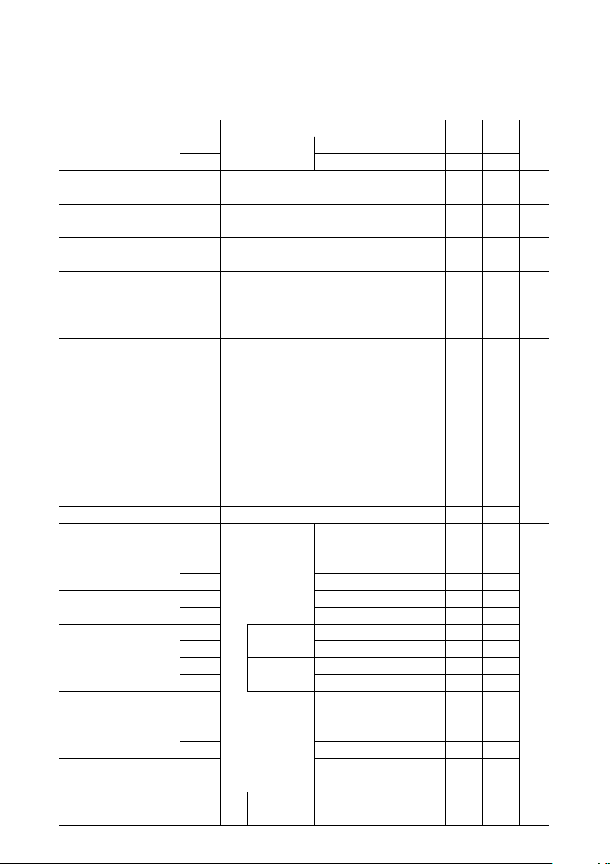
AC Characteristics (DTMF)
(
VDD = 2.5 V to 3.6 V, Ta = –40°C to +85°C)
Parameter Min. Unit
V
Transmit Level
Transmit Signal Level
Relative Value
V
V
DTTL
DTTH
DTDF
AOUT, R1 = R3
High-group tone/low-group tone
ConditionSymbol Typ. Max.
Low-group tone
High-group tone
–16.5
–15.5
0
–14.5
–13.5
–12.5
–11.5
1
2
dBm
*1
dB
Transmit Frequency
Deviation
Transmit Signal
Distortion Rate
DTG1 to DTG4 Input Data
Setup Time
DTG1 to DTG4 Input Data
Hold Time
Receive Detect Level
Receive Reject Level
Receive Frequency
Detect Band
Receive Frequency
Reject Band
Allowable Receive Level
Difference
Allowable Receive
Noise Level ratio
f
DDT
THD
t
SDT
t
HDT
V
DETDT
V
REJDT
f
DETDT
f
REJDT
V
TWIST
V
N/S
With respect to the nominal frequency
Harmonics/Fundamental frequency
DT
See Fig. 2.
See Fig. 2.
For each single tone
For each single tone
With respect to the nominal frequency
With respect to the nominal frequency
High-group tone/low-group tone
Noise (0.3 kHz to 3.4 kHz)
level/tone level
–1.5
—
250
250
–46
—
—
±3.8
–6
—
—
—
—
—
—
—
—
—
—
–12
+1.5
–23
—
—
–10
–60
±1.5
—
+6
—
%
dB
ns
dBm
*1
%
dB
Dial Tone Reject Ratio
Signal Repetition Time
Tone Time for Detect
Tone Time for No Detect
Output Delay Time
Interdigit Pause Time
Acceptable Drop Out Time
SP Delay Time
Output Trailing Edge
Delay Time
V
REJ400
t
t
t
t
t
t
t
G11
t
G12
t
G21
t
G22
t
t
t
t
t
SP1
t
SP2
t
t
D1
D2
C1
C2
S1
S2
P1
P2
B1
B2
380 Hz to 420 Hz
DTTIM = "1"
DTTIM = "0"
DTTIM = "1"
37
120
70
49
—
—
—
—
—
—
—
—
See Fig. 1
DTTIM = "0"
I1
I2
Normal
condition *2
Just after
mode change *3
DTTIM = "1"
DTTIM = "0"
DTTIM = "1"
DTTIM = "0"
DTTIM = "1"
DTTIM = "0"
DTTIM = "1"
DTTIM = "0"
DTTIM = "1"
DTTIM = "0"
DTTIM = "1"
DTTIM = "0"
> 80 ms
t
S
> 44 ms
t
S
DTTIM = "1"
DTTIM = "0"
34
—
—
30
20 42
30
21
—
—
6
1
21
15 27
—
—
—
45
32
4830 77
3520 62
—
—
—
—
8
1.7
29
21
—
24
9
57
ms
—
—
10
3
10
3
35
7/21
 Loading...