OKI MSM7652GS-2K Datasheet

Preliminary
¡ Semiconductor MSM7652
This version: Jun. 1998
¡ Semiconductor
MSM7652
NTSC/PAL Digital Video Encoder
GENERAL DESCRIPTION
The MSM7652 is a digital NTSC/PAL encoder. By inputting digital image data conforming to
ITU Rec. 656 or ITURBT 601, it outputs selected analog composite video signals, analog S video
signals or Y, R-Y, B-Y signals. For the scanning system, interlaced or noninterlaced mode can be
selected.
Since the MSM7652 is provided with pins dedicated to overlay function, text and graphics can
be superimposed on a video signal.
In addition, this encoder has an internal 10-bit DAC. So, when compared with using a conventional
analog encoder, the number of components, the board space, and points of adjustment can
greatly be reduced, thereby realizing a low cost and high-accuracy system.
The MSM7652 provides the optional functions such as Closed Caption Signal Generation
Function.
The host interface provided conforms to Philips's I2C specifications, which reduces
interconnections between this encoder and mounting components.
The internal synchronization signal generator (SSG) allows the MSM7652 to operate in master
mode.
FEATURES
• Video signal system: NTSC/PAL
• Scanning system: interlaced/noninterlaced (NTSC : 262 lines/PAL : 312 lines)
• Input digital level: conforms to ITU-R601 (CCIR601)
• Input-output timing: conforms to ITU Rec. 656 or ITURBT 624-4
• Input signal sampling ratio : Y:Cb:Cr = 4:2:2
• Supported input formats
· ITU Rec. 656
· YCbCr 27 MHz format (8-bit input)
· ITU-R601 13.5 MHz (8-bit (Y) + 8-bit (CbCr) input)
• Output video signals
· NTSC/PAL composite video signals and S video signals
· Y, R-Y, B-Y analog signals (selectable)
• Sampling frequency : 27 MHz
• Internal SSG circuit (Can operate as a master in other operation modes than CCIR Rec. 656
mode)
• Internal 3ch 10-bit DAC
• 3-bit title graphics can be displayed
• Color bar function
•I2C-bus host interface function
• 3.3 V single power supply (each I/O pin is 5 V tolerable)
• Closed caption function
• Package
56-pin plastic QFP (QFP56-P-910-0.65-2K) (Product name: MSM7652GS-2K)
1

MSM7652 ¡ Semiconductor
APPLICATIONS
• Video CD
• Video game equipment
• Electronic still cameras
• Video file systems
• Video cameras
• Videophones
• Multimedia equipment
• Video printers
• Videoconferencing systems
• Scanners
• Video graphics boards
2
¡ Semiconductor MSM7652
3
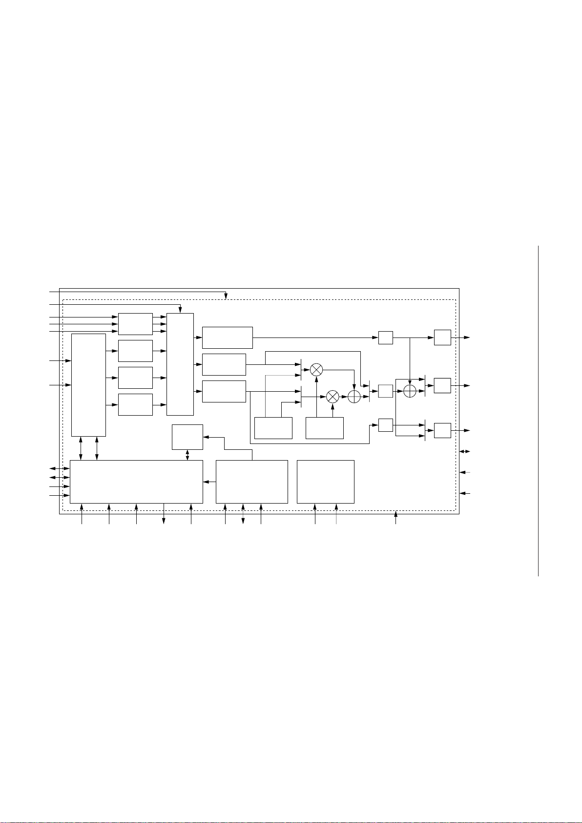
BLOCK DIAGRAM
Sync Generator & Timing Controller
Prologue
Block
I2C Control logic Test Control logic
IPF
Overlay
Control
YUV color
Generator
RESET_L
Black &
Blank Pedestal
Interpolator
+ LPF
Interpolator
+ LPF
Color Burst
Generator
Y Level
converter
U Level
converter
V Level
converter
Closed
Caption
Block
OLC
OLG
OLB
CD[7:0]
CLKX2
MODE
CLKX1O CLKSEL
SCL SDA
ADRS
Subcarrier
Generator
TENB TEST1
CVBSO (B-Y)
MSSEL[2:1]
BLANK_L
HSYNC_L
VSYNC_L
YD[7:0]
OLR
DAC
IPF
YA (Y)
DAC
IPF
IPF = Interpolation Filter
CA (R-Y)
DAC
VREF
FS
OUTSEL
COMP

MSM7652 ¡ Semiconductor
PIN CONFIGURATION (TOP VIEW)
DV
DD
MS
SDA
SCL
ADRS
RESET_L
MODE
OLC
OLR
OLG
10
DD
AGND
YA (Y)
AV
DGND
56
55
54
53
1
2
3
4
5
6
7
8
9
DD
AV
CVBSO (B-Y)
52
51
AGND
CA (R-Y)
50
49
COMP
48
FS
47
VREF
46
TENB
45
TEST1
44
DGND
43
42
41
40
39
38
37
36
35
34
33
DV
DD
SEL2
SEL1
CLKSEL
CD0
CD1
CD2
CD3
CD4
CD5
OLB
CLKX1O
OUTSEL
DV
DD
11
12
13
14
15
DGND
16
17
VSYNC_L
HSYNC_L
18
19
20
YD6
YD7
BLANK_L
NC : No-connection pin
56-Pin Plastic QFP
21
NC
22
YD5
23
YD4
24
YD3
25
YD2
26
YD1
27
YD0
32
31
30
29
28
DGND
CD6
CD7
CLKX2
DV
DD
4
¡ Semiconductor MSM7652
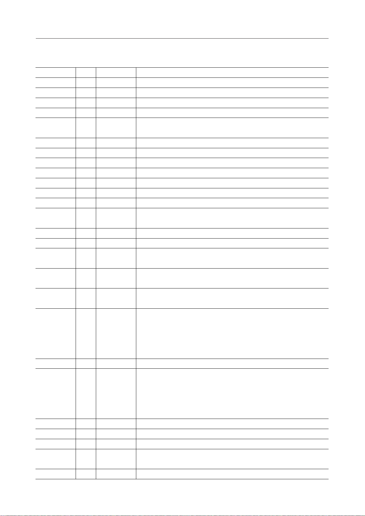
PIN DESCRIPTIONS (1/2)
Pin I/O Symbol Description
1DV
DD
2IMS
3 I/O SDA I2C interface data bus
4 I SCL I
5 I ADRS
6 I RESET_L System reset signal. Negative porality
7 I MODE Broadcasting mode select pin. "0" : NTSC/"1" : PAL. Pulled down
8 I OLC
9 I OLR Overlay text color (Red component)
10 I OLG Overlay text color (Green component)
11 I OLB Overlay text color (Blue component)
12 O CLKX1O 13.5 MHz divided clock output signal
13 I OUTSEL
14 DV
DD
15 DGND Digital GND
16 I/O VSYNC_L
17 I/O HSYNC_L
18 I BLANK_L
19, 20 I YD7 to YD6
21 NC Not connected
22 to 27 I YD5 to YD0
28 DGND Digital GND
29 DV
DD
30 I CLKX2 Clock input pin (27 MHz)
31 to 38 I/O CD7 to CD0
39 I CLKSEL
3.3 V digital power supply
Selects between Master and Slave at 27 MHz or 13.5 MHz YCbCr operation. Pulled down
2
C interface clock bus
2
C-bus Slave address setting pin ("0" : 1000100 / "1" : 1000110).
I
Pulled down
Transparent control signal. "1" indicates overlay signal. Normally fixed to "0".
. Normally fixed to "0".
. Normally fixed to "0".
. Normally fixed to "0".
Video output signal format select pin. "0" : Y/C & Composite signal,
"1" : Y/B-Y/R-Y (component) signal. Pulled down
3.3 V digital power supply
Vertical sync signal input/output pin (ITU656: O, YCbCr: I/O)
Negative polarity
Horizontal signal input/output pin (ITU656 : O, YCbCr: I/O)
Negative polarity
Composite blank signal. Negative polarity. See the description on page 15
for the operating requirement.
MSB 2 bits of 8-bit digital image data input pins (for ITU656 and
YCbCr 27 MHz). Level conforms to ITU-601.
MSB 2 bits of 8-bit digital image luminance signal input pins (for YCbCr).
Level conforms to ITU-601.
YD7 is MSB.
LSB 6 bits of 8-bit digital image data input pins (for ITU656 and
YCbCr 27 MHz). Level conforms to ITU-601.
LSB 6 bits of 8-bit digital image luminance signal input pins (for YCbCr).
Level conforms to ITU-601.
YD0 is LSB.
3.3 V digital power supply
8bit digital image chrominance signal data input pins (13.5 MHz mode).
Level conforms to ITU-601. Fixed to "0" for ITU Rec. 656, 27 MHz-YCbCr mode.
Operation mode select pin. "0" : 27 MHz mode / "1" : 13.5 MHz mode.
5
MSM7652 ¡ Semiconductor
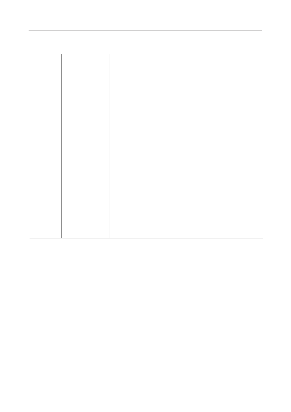
PIN DESCRIPTIONS (2/2)
Pin I/O Symbol Description
40 I SEL1
Enable pin. Normally fixed to "0". Sleep mode "1" with TEST1 = "0"
(See Page 32 for details)
41 I SEL2
42 DV
DD
Pulled down
3.3 V digital power supply
43 DGND Digital GND
Interface select pin. ITU656 : "0", YCbCr 27 MHz : "1" (See Page 32 for details)
44 I TEST1
45 I TENB
Input pin1 for testing. Normally fixed to "0". (See Page 32 for details)
Pulled down
Input pin2 for testing.
Normally fixed to "0"
.
Pulled down
46 I/O VREF Reference voltage for DAC
47 I FS DAC full scale adjustment pin.
48 I COMP DAC phase complement pin.
49 AGND Analog GND
50 O CA
51 AV
DD
52 O CVBSO
Analog color chrominance signal output pin or component B-Y signal
output pin.
3.3 V analog power supply
Analog composite signal output pin or component R-Y signal output pin.
53 AGND Analog GND
54 O YA Analog luminance signal output pin or component Y signal output pin.
55 AV
DD
3.3 V analog power supply
56 DGND Digital GND
6
¡ Semiconductor MSM7652
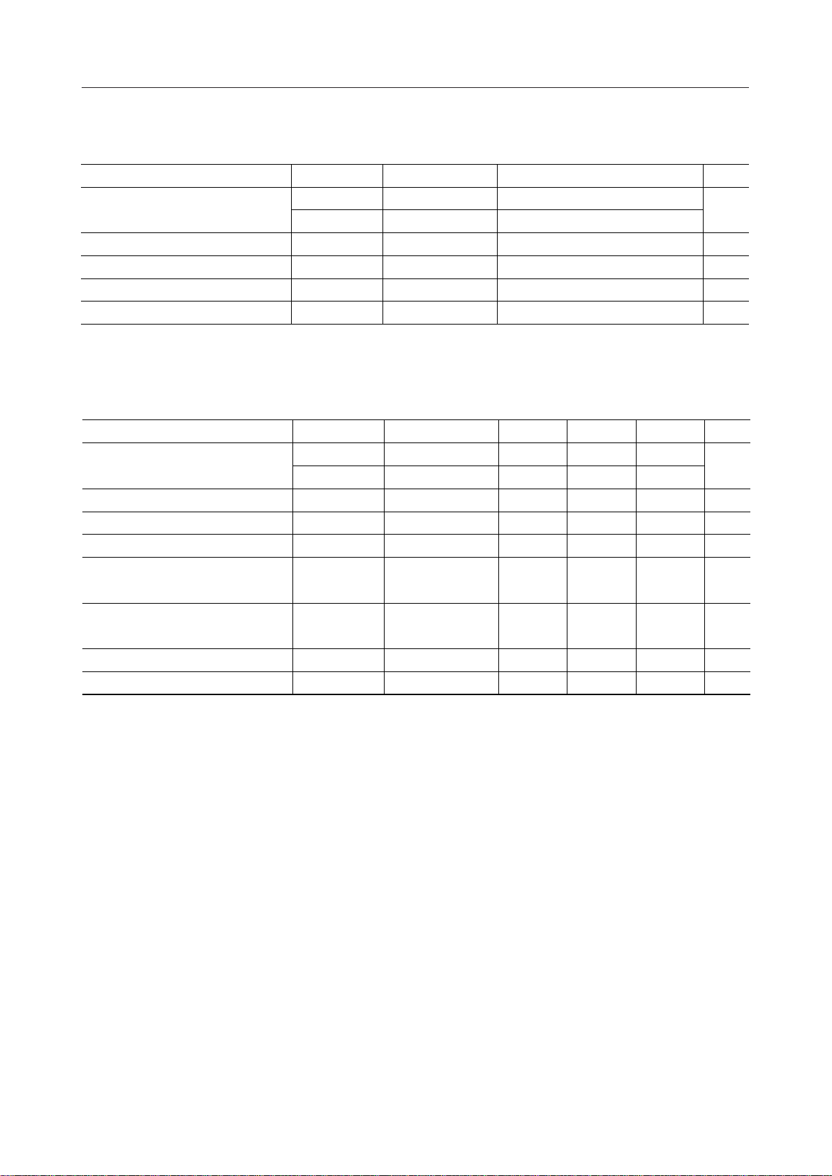
ABSOLUTE MAXIMUM RATINGS
Parameter
Power Supply Voltage
Input Voltage
Analog Output Current
Power Consumption
Storage Temperature
Symbol
DV
DD
AV
DD
V
I
I
O
P
W
T
STG
Condition
—
—
= 3.3 V
DV
DD
—
—
—
RECOMMENDED OPERATING CONDITIONS
Parameter
Power Supply Voltage (*1)
"H" Level Input Voltage
"L" Level Input Voltage
Operating Temperature 1 Ta1
Operating Temperature 2 Ta2
Symbol
DV
DD
AV
DD
V
IH
V
IL
Condition
—
—
—
—
DVDD = AVDD = 3.3 V
DVDD = AVDD = 3.3 V
DA output load = 37.5 W
Min.
3.0
3.0
2.2
—
0
Rating
Unit
–0.3 to +4.5
V
–0.3 to +4.5
–0.3 to +5.5
50
600
–55 to +150
Typ.
3.3
Max.
3.6
V
mA
mW
°C
Unit
V
3.3
—
—
25 ˚C
3.6
—
0.8
70
V
V
25 ˚C065
DVDD = AVDD = 3.3 V,
External Reference Voltage Vrefex
Ta = 25˚C
1.25 V——
DA Current Setting Resistance Riadj (*2) 385 W——
DA Output Load Resistance R
L
(*3) 75 W——
(*1) Supply an equal voltage to both DVDD and AVDD.
(*2) A volume control resistor of approx. 500 W is recommendable for adjusting the output
current. When a DA converter analog output is terminated with a 37.5 W load, Riadj
= approx. 192 W.
(*3) Indicates the value when Riadj = 385 W (typical value).
7
MSM7652 ¡ Semiconductor
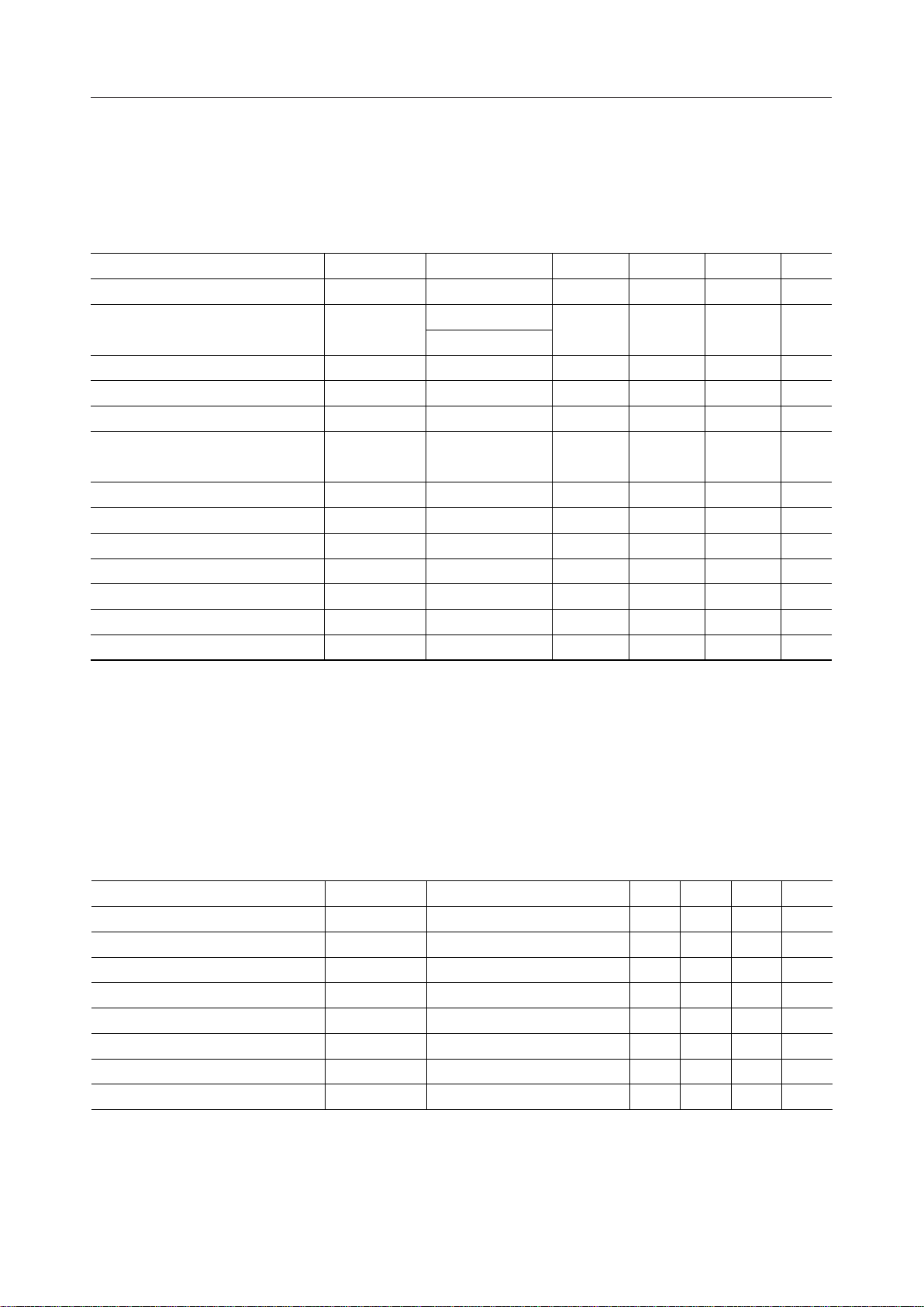
ELECTRICAL CHARACTERISTICS
DC Characteristics
(Ta = 0 to 70°C, DV
Parameter Symbol
"H" Level Output Voltage V
"L" Level Output Voltage V
Input Leak Current I
Output Leak Current I
Power Supply Current (operating) I
V
OH
OL
O
DDO
I
Condition
= –4 mA (*1)
I
OH
= 4 mA (*1)
I
OL
IOL = 6 mA (*2)
VI = GND to DV
DD
VI = GND to DVDD (*3)
— 120 mA— 140
= 3.3 V ±0.3 V, AVDD = 3.3 V ±0.3 V)
DD
Min.
0.7V
—
DD
Typ.
—
—V
Max.
—
0.4
— mA–10 +10
— mA–10 +10
Unit
RESET_L = "L"
Power Supply Current (standby) I
Power Supply Current (Sleep mode)
DDS
I
DDSM
I2 C-bus SDA Output Voltage SDAV
I2C-bus SDA Output Current SDAI
CLKX2 = 0 MHz
SEL2 = "H" 0.05 mA0.03 0.5
Low level, IOL = 3 mA
L
O
During Acknowledge
60 mA—65
—V0 0.4
—mA3—
Internal Reference Voltage Vrefin — 1.25 V——
DA Output Load Resistance R
L
—75W
Integral Linearity SINL — ±2 LSB
Differential Linearity SDNL — ±1 LSB
(*1) VSYNC_L, HSYNC_L, CD[7:0]
(*2) CLKX1O
(*3) SDA
AC Characteristics
Parameter Symbol Condition Min. Typ. Max. Unit
CLKX2 Cycle Time T
Input Data Setup Time
Input Data Hold Time
Output Delay Time
CLKX1O Delay Time
2
C-bus Clock Cycle Time t
I
2
C-bus High Level Cycle t
I
2
C-bus Low Level Cycle t
I
S
t
s1
t
h1
t
d1
t
d2
C_SCL
H_SCL
L_SCL
(Ta = 0 to 70°C, DV
—
—
—
—
—
Rpull_up = 4.7 kW
= 3.3 V ±0.3 V, AVDD = 3.3 V ±0.3 V)
DD
——
36.4 ns
7ns
5ns
525ns
525ns
200
100 —
100
—
—
—
—
——
—ns
——
—
—
nsRpull_up = 4.7 kW
nsRpull_up = 4.7 kW
8
¡ Semiconductor MSM7652
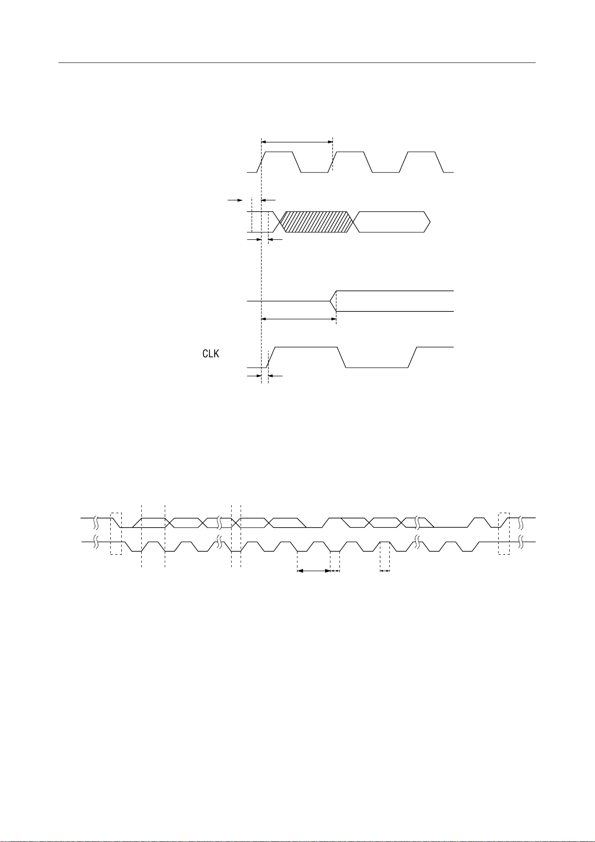
INPUT/OUTPUT TIMING
Input timing
TS
CLKX2
ts1
td1
Invalid data
th1
valid data
HSYNC_L,
VSYNC_L, BLANK_L,
YD, CD, MS, MODE,
OLR, OLG, OLB, OLC
Output timing
HSYNC_L, VSYNC_L
CLKX1O
td2
I2C-bus Interface Input/Output Timing
The following figure shows I2C-bus basic input/output timing.
SDA
SCL
S
Start Condition
Data Line Stable: Data Valid
MSB
12 789
Change of Data Allowed
ACK
t
C_SCL
I2C-bus Basic Input/Output Timing
12
t
L_SCL
t
H_SCL
3-8
9
ACK
P
Stop Condition
9

MSM7652 ¡ Semiconductor
BLOCK FUNCTIONAL DESCRIPTION
1. Prologue Block
This block separates input data at the ITU Rec.656 format into a luminance signal (Y) and a
chrominance signal (Cb & Cr), and also generates information concerning sync signals
HSYNC_L, VSYNC_L, and BLANK_L.
This block separates input data at the 27 MHz YCbCr (8-bit input) format into a luminance
signal (Y) and a chrominance signal (Cb & Cr).
This block separates input data at the 13.5 MHz YCbCr (16-bit input) format into a chrominance
signal Cb and a chrominance signal Cr.
Of the processed input data, luminance and chrominance signals other than valid pixel data
are replaced by 8'h10 and 8'h80 respectively.
2. Y Limiter Block
This block limits the luminance input signal by clipping the lower limit of an input signal outside
the ITU601 Standard
• Signals are limited to YD = 16 when YD < 16.
• Signals are limited to TD = 254 when YD (input during a valid pixel period) = 255.
In other cases, signals are fed as is to next processing.
3. C Limiter Block
This block limits the chrominance signal by clipping the upper and lower limits of the input
signal outside the ITU601 Standard.
CD = 1 when CD = 0 is input during a valid pixel period.
CD = 254 when CD = 255 is input during a valid pixel period.
• Y Level Converter
Converts ITU-601 standard luminance signal level to DAC digital input level.
• U Level Converter
Converts ITU-601 standard chrominance signal level to DAC digital input level.
• V Level Converter
Converts ITU-601 standard chrominance signal level to DAC digital input level.
• YUV Color Generator
This block generates luminance and chrominance signals from over lay color signals OLR,
OLG and OLB. Control signals (CR [2:0] ) control the output content (overlay or color bar) and
output level (100%, 75%, 50%, 25%).
• Overlay Control
This block selects input image data or YUV Color Generator output signals.
It is determined by the level of the control signal (OLC, CR [2]), as shown below: (x : don't care)
CR [2] = 1, OLC = x: Selects color bar signal (YUV Color Generator output signal).
CR [2] = 0, OLC = 1: Selects overlay signal (YUV Color Generator output signal).
CR [2] = 0, OLC = 0: Selects input image data.
10

¡ Semiconductor MSM7652
• Black & Blank Pedestal
This block adds sync signals at the luminance side to luminance signals.
• Interpolator + LPF
This block executes data interpolation and the elimination of high frequency components by
LPF for input chrominance signals.
•I2C Control Logic
This is the serial interface block based on I2C standard of Phillips Corporation.
Internal registers MR and CR can be set from the master side.
When writing to the internal registers other than MR [1] (black level control) and CR [1:0]
(overlay level), written contents are immediately set to them. It is during the vertical blanking
period that written contents are set to MR [1] and CR [1:0].
• Sync Generator & Timing Controller
This block generates sync signals and control signals.
This block operates in slave mode, which performs external synchronization, and in master
mode, which internally generates sync signals.
• Color Burst Generator
Outputs U and V components of amplitude of burst signals.
• Subcarrier Generator
Executes color subcarrier generation.
• Interpolation Filter (IPF)
This block performs upsampling at CLKX2 for luminance signals and chrominance signals
modulated with CLKX1 divided from CLKX2. Interpolation processing is executed in this
process.
• Closed Caption Block
This block generates the signal for closed caption.
11
 Loading...