OKI MSM7650GS-BK Datasheet

E2F0003-27-X1
¡ Semiconductor MSM7650
¡ Semiconductor
This version: Jan. 1998
Previous version: Oct. 1997
MSM7650
NTSC/PAL Digital Encoder
GENERAL DESCRIPTION
The MSM7650 is a digital NTSC/PAL encoder. By inputting digital image data conforming to
CCIR Rep624-4, it outputs analog composite video signals and analog S video signals. For the
scanning system, interlaced or noninterlaced mode can be selected.
Since the MSM7650 is provided with pins dedicated to overlay function, text and graphics can
be superimposed on a video signal.
In addition, this encoder has an internal 9-bit DAC. So, when compared with using a conventional
analog encoder, the number of components, the board space, and points of adjustment can
greatly be reduced, thereby realizing a low cost and high-accuracy system.
The host interface provided conforms to Philips's I2C specifications, which reduces
interconnections between this encoder and mounting components.
The internal synchronization signal generator (SSG) allows the MSM7650 to operate in master
or slave mode.
FEATURES
• Video signal system: NTSC/PAL
• Scanning system: interlaced/noninterlaced
• Input digital level: conforms to ITU-601 (CCIR601)
• Input-output timing: conforms to CCIR Rep 624-4
• Input signal (sampling ratio)
Y:Cb:Cr (4:2:2/4:1:1)
• Supported sampling rates
• NTSC 4Fsc (14.32 MHz)
• NTSC ITU-R601 (13.5 MHz)
• NTSC Square Pixel (12.27 MHz)
• PAL ITU-R601 (13.5 MHz)
• PAL Square Pixel (14.75 MHz)
• Internal SSG circuit (internally generates sync signals)
• Operation by external synchronization possible
• Internal 3ch 9-bit DAC (samples by double frequency)
• 3-bit title graphics can be displayed
•I2C-bus host interface function
• Package
80-pin plastic QFP (QFP80-P-1420-0.80-BK) (Product name: MSM7650GS-BK)
1/34

¡ Semiconductor MSM7650
APPLICATIONS
• Video game equipment • CD-ROM
• Electronic still camera • Video graphics board
• Video printer • Videophone
• Video camera • Video conference system
• Scanner • Multimedia equipment
• Image file system • Digital VTR
2/34
¡ Semiconductor MSM7650
3/34
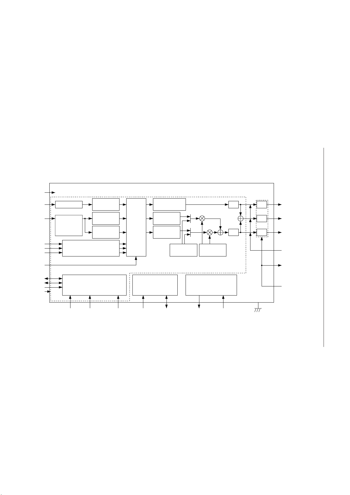
BLOCK DIAGRAM
Y Limitter
Y Level
Converter
Overlay
Control
Black &
Blank Pedestal
IPF
C Limitter
&
UV Selector
YD[7:0]
CD[7:0]
OLR
OLG
OLB
OLC
VSYNC_L
HSYNC_L
BLANK_L
CLKX1
U Level
Converter
Interpolator
+ LPF
V Level
Converter
Interpolator
+ LPF
YUV Color
generator
DAC
DAC
IPF DAC
Color Burst
Generator
Subcarrier
Generator
Sync Generator
&
Timing Controller
I2C Control Logic Test Control Logic
YA
CVBSO
CA
CT [8:0]
CLKX2O
RESET_L
TEST[4:1]TOUT[2:1]
SDASCLMODE[2:0]INTERLACEMS
CLKX2
X
¡ Semiconductor MSM7650
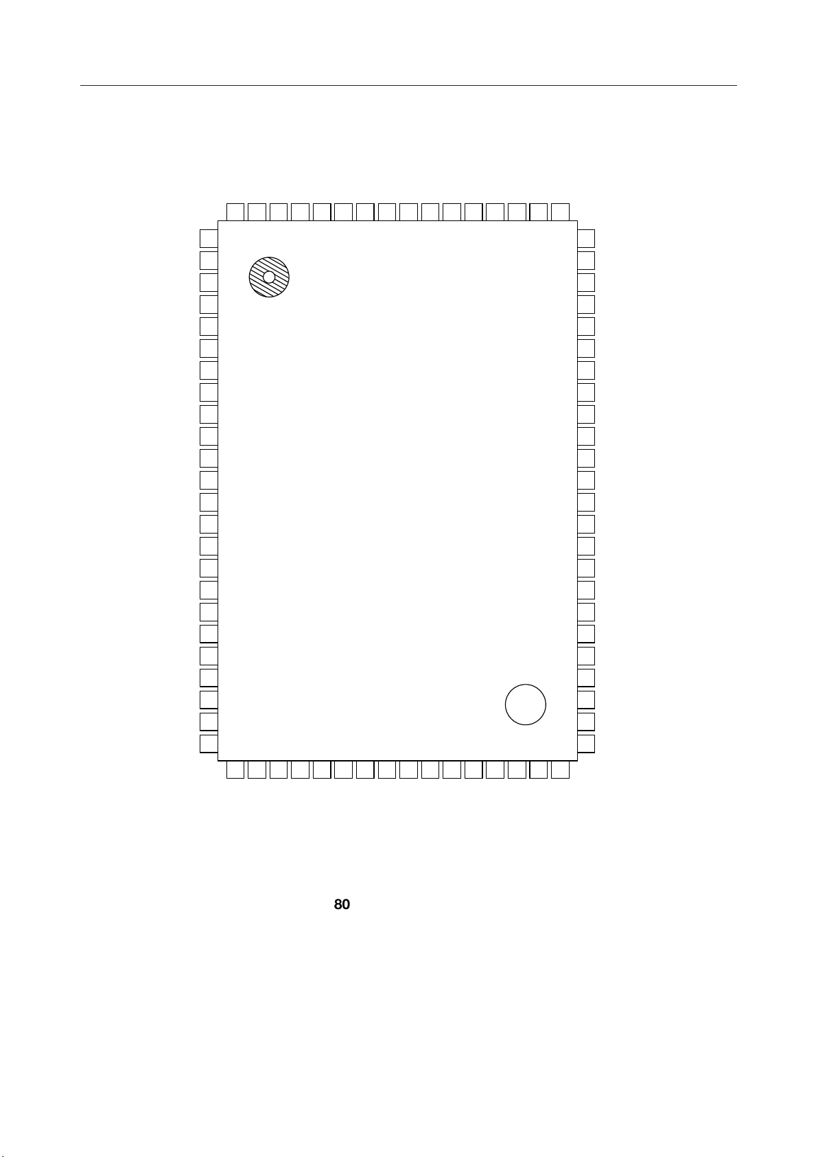
PIN CONFIGURATION (TOP VIEW)
CD7
CD6
CD5
CD4
CD3
CD2
CD1
CD0
YD7
YD6
YD5
YD4
YD3
YD2
YD1
YD0
806579
78
77
76
75
74
73
72
71
70
69
68
67
66
V
DD5
V
DD3
GND
VSYNC_L
HSYNC_L
BLANK_L
CLKX1
CLKX2
CLKX2O
X_L
V
DD3
GND
CT8
CT7
CT6
CT5
CT4
CT3
CT2
CT1
CT0
V
DD5
GND
1
2
3
4
5
6
7
8
9
10
X
11
MSM7650
12
13
14
15
16
17
18
19
20
21
22
23
24
64
V
63
V
62
GND
61
OLR
60
OLG
59
OLB
58
OLC
57
MODE[0]
56
MODE[1]
55
MODE[2]
54
INTERLACE
53
MS
52
RESET_L
51
SCL
50
SDA
49
ADRS
48
TOUT2
47
TOUT1
46
TEST4
45
TEST3
44
TEST2
43
TEST1
42
GND
41
V
DD5
DD3
DD3
254026
NC
DD3
V
27
VREF
28
29
30
31
32
FS
AGNDYAAGND
COMP
NC : No-connection pin
80-Pin Plastic QFP
33
DDAVDD
AV
34
35
36
AGND
CVBSO
37
CA
38
DD
AV
39
GND
NC
4/34
¡ Semiconductor MSM7650
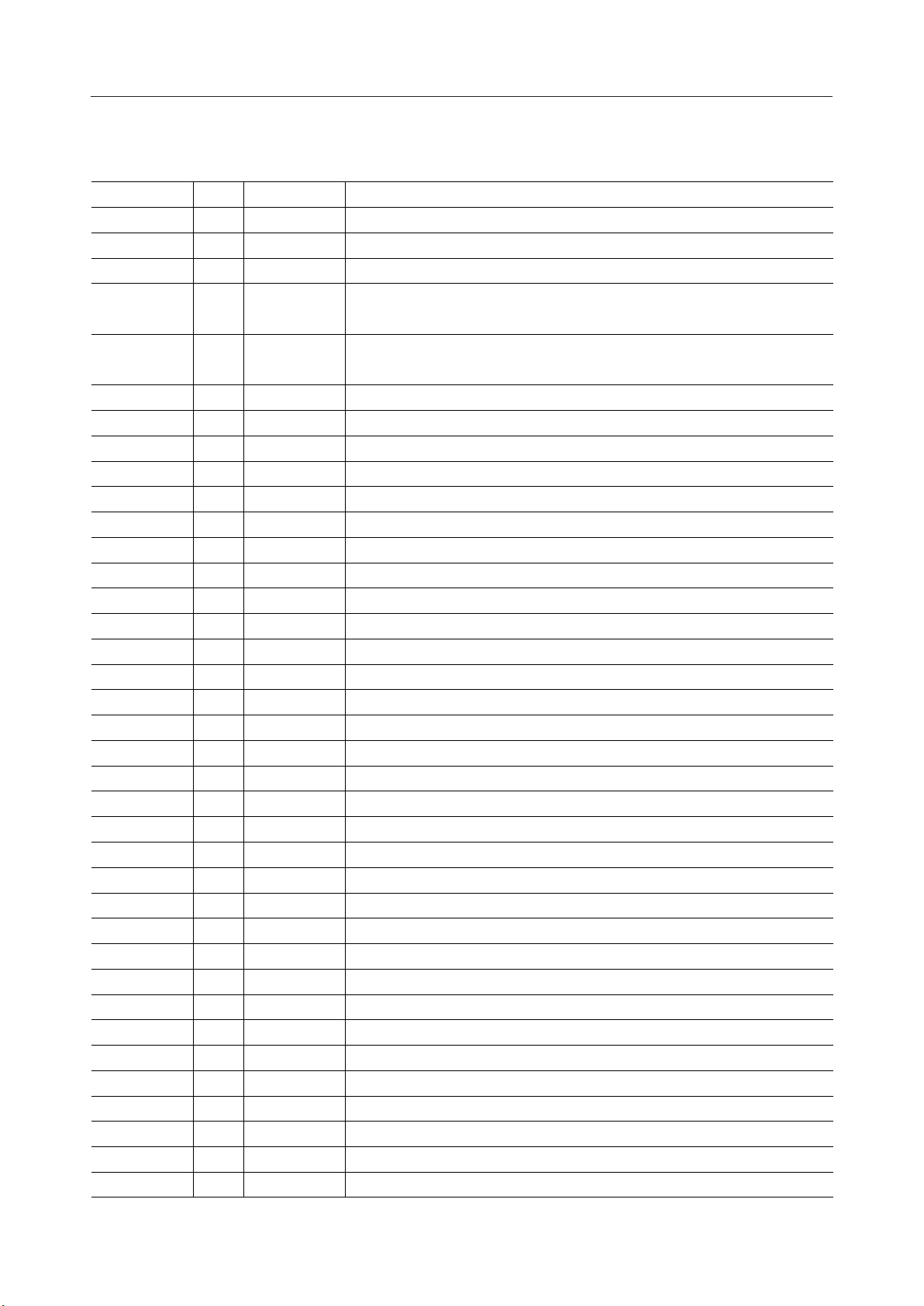
PIN DESCRIPTIONS (1/2)
Pin
1
2
3
4
5
6
7
8
9
10
11
12
13
14 to 22
23
24
25
26
27
28
29
30
31
32
33
34
35
36
37
38
39
40
41
42
43
44
45
I/O
I/O
I/O
I
I
I
O
I
O
I
I/O
I
I
I
O
O
O
I
I
Symbol
V
DD5
V
DD3
GND
VSYNC_L
HSYNC_L
BLANK_L
CLKX1
CLKX2
CLKX2O
X
X_L
V
DD3
GND
CT8 to CT0
V
DD5
GND
V
DD3
NC
VREF
FS
COMP
AGND
YA
AGND
AV
DD
AV
DD
CVBSO
AGND
CA
AV
DD
GND
NC
V
DD3
GND
TEST1
TEST2
TEST3
Description
5.0V power supply
3.3V power supply
Digital GND
Vertical sync signal
Polarity is negative. Output pin in master mode; input pin in slave mode.
Horizontal sync signal
Polarity is negative. Output pin in master mode; input pin in slave mode.
Composite blank signal. Polarity is negative.
Pixel clock input pin
Double pixel clock input pin
Double pixel clock output pin
Test pin. Normally, fixed to "0".
Test pin
3.3V power supply
Digital GND
Input pin for testing. Normally, fixed to "0" or "1".
5.0V power supply
Digital GND
3.3V power supply
Not connected
Reference voltage for DAC
DAC full scale adjustment pin
DAC phase compensation pin
Analog GND
Analog luminance signal output pin
Analog GND
Analog power supply
Analog power supply
Analog composite video signal output pin
Analog GND
Analog chrominance signal output pin
Analog power supply
Digital GND
Not connected
3.3V power supply
Digital GND
Input pin 1 for testing. Normally, fixed to "0".
Input pin 2 for testing. Normally, fixed to "0".
Input pin 3 for testing. Normally, fixed to "0".
5/34
¡ Semiconductor MSM7650
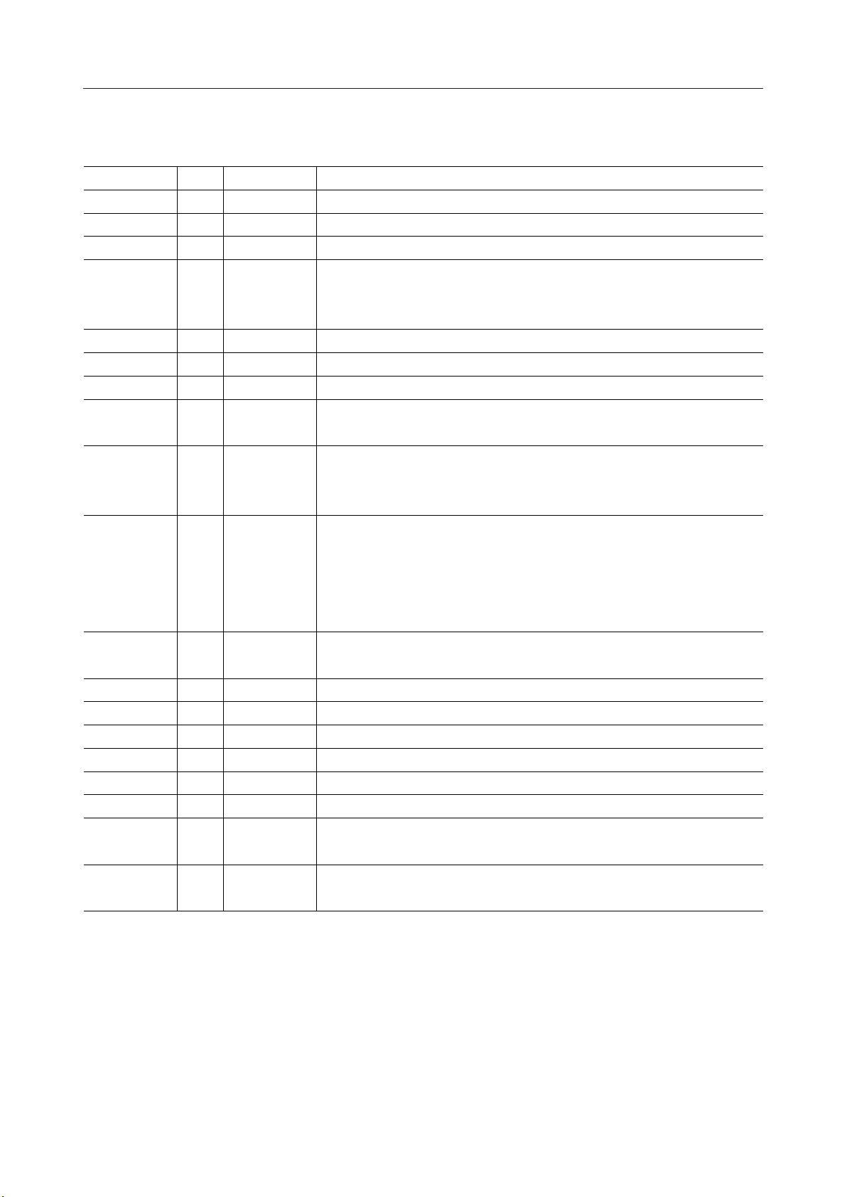
PIN DESCRIPTIONS (2/2)
Pin
46
47
48
49
50
51
52
53
54
55 to 57
58
59
60
61
62
63
64
65 to 72
73 to 80
I/O
I
O
O
I
I/O
I
I
I
I
I
I
I
I
I
I
I
Symbol
TEST4
TOUT1
TOUT2
ADRS
SDA
SCL
RESET_L
MS
INTERLACE
MODE[2]
to MODE[0]
OLC
OLB
OLG
OLR
GND
V
DD3
V
DD5
YD0 to YD7
CD0 to CD7
Description
Input pin 4 for testing. Normally, fixed to "0".
Output pin for testing
Output pin for testing
2
C-bus subaddress setting pin. One of two addresses switchable can be
I
selected as subaddress.
1: 1000110/0: 1000100
2
I
C-bus data pin
2
I
C-bus clock pin
System reset pin. "1" at an open state by an internal pull-up resistor
Operation mode select signal pin for synchronization circuit.
1: master/0: slave. "1" at an open state by an internal pull-up resistor
Interlace/noninterlace select signal pin.
1: interlaced/0: noninterlaced. "1" at an open state by an internal pull-up
resistor
Video mode select pins
These pins are valid when MR[7] is "1".
000: NTSC CCIR
100: PAL CCIR
001: NTSC Square Pixel
101: PAL Square Pixel
010: NTSC 4Fsc
"000" at an open state by an internal pull-down resistor
Transparent control signal
Overlay signal is displayed when this pin is "H".
Overlay text color (Blue component)
Overlay text color (Green component)
Overlay text color (Red component)
Digital GND
3.3V power supply
5.0V power supply
Digital image luminance signal data input pin
Level is based on ITU-601. YD7 is MSB.
Digital image chrominance signal data input pin
Level is based on ITU-601. CD7 is MSB.
6/34
¡ Semiconductor MSM7650
ABSOLUTE MAXIMUM RATINGS
Parameter
Power Supply Voltage
Input Voltage
Analog Output Current
Power Consumption
Storage Temperature
Symbol
V
DD5
V
DD3
AV
DD
V
I
I
O
P
W
T
STG
Condition
Ta=25°C
Ta=25°C
Ta=25°C
Ta=25°C
—
—
—
RECOMMENDED OPERATING CONDITIONS
Parameter
Power Supply Voltage
Power Supply Voltage
High Level Input Voltage
Symbol
V
DD5
V
DD3
AV
DD
GND
AGND
V
IH1
V
IH2
V
IH3
Condition
Ta=25˚C
Ta=25˚C
Ta=25˚C
Ta=25˚C
Ta=25˚C
SDA, CLKX1,
Except CLKX2,
Ta=25˚C
SDA, Ta=25˚C — V0.8
CLKX1,CLKX2,
Ta=25˚C
Min.
4.5
3.0
3.0
—
—
2.2
V
DD5
Rating
–0.3 to +7
–0.3 to +4.5
–0.3 to +4.5
–0.3 to V
800
–55 to +150
Typ.
5.0
3.3
3.3
0.0
0.0
40
—
—V2.4
DD5
+0.3
Max.
5.5
3.6
3.6
—
—
V
DD5
V
DD5
V
DD5
Unit
V
V
mA
mW
°C
Unit
V
V
V
Low Level Input Voltage
V
IL
Operating Temperature Range Ta — — ˚C
—
0.0
0.0
—
0.5
70
V
External Reference Voltage (*1) Vrefex — 1.25 V——
DA Current Setting Resistance (*2) Riadj — 330 W——
DA Output Load Resistance R
L
—75W——
(*1) When external reference voltage is not supplied, internal reference voltage is as
follows.
Internal Reference Voltage Vrefin — — V1.15 1.45
(*2) A volume control resistor of approx. 500W is recommendable for adjusting the output
current.
7/34
¡ Semiconductor MSM7650
ELECTRICAL CHARACTERISTICS
DC Characteristics
(Ta=0 to +70°C, V
Parameter Symbol
High Level Output Voltage V
Low Level Output Voltage V
Input Leak Current I
Output Leak Current I
V
OH
OL
I
O
Condition
=–4mA (*1)
I
OH
I
=–8mA (*2)
OH
=4mA (*1)
I
OL
IOL=8mA (*2)
VI=GND to V
VI=GND to V
DD5
DD5
(*3)
Min.
0.8V
DD5
0
=3.3V±0.3V, V
DD3
Typ.
—
—V
— mA–10 10
— mA–10 10
DD5
Max.
V
DD5
0.6
=5V±10%)
Unit
CLKX1=13.5MHz
Power Supply Current (operating) I
DDO
CLKX2=27.0MHz
120 mA— 140
RESET_L="L"
Power Supply Current (standby) I
DDS
I2 C-bus SDA Output Voltage SDAV
I2C-bus SDA Output Current SDAI
CLKX1=CLKX2=0Hz
L
O
Low level, IOL=3mA
During Acknowledge
65 mA—80
—V0 0.4
—mA3—
Internal Reference Voltage Vrefin — — V1.15 1.45
DA Output Load Resistance R
L
—75W
Integral Linearity SINL ±2 LSB
Differential Linearity SDNL ±1 LSB
(*1) HSYNC_L, VSYNC_L, SDA, TO, CT[7:0]
(*2) CLKX2O
(*3) SDA
8/34
¡ Semiconductor MSM7650
AC Characteristics
Parameter Symbol Condition Min. Typ. Max. Unit
CLKX Cycle Time T
Input Data Setup Time
Input Data Hold Time
Output Delay Time
CLKX2O Delay Time
Clock Cycle Time t
Clock Duty Cycle t
Low Level Cycle t
C_SCL
D_SCL
L_SCL
(Ta=0 to +70°C, V
PAL Square Pixel 67.8 ns
NTSC 4Fsc 69.8 ns
S
NTSC Square Pixel 81.5 ns
ITU-RS601 74.1 ns
t
s1
t
h1
t
d1
t
d2
—
—
—
—
=3.3V±0.3V, V
DD3
—
—
—
—
7.03 ns
9.48 ns
18.35 24.12 ns
7.69 9.53 ns
—
—
—
—
200
——
50 %
100
=5V±0.5V)
DD5
—
—
—
—
—
—
nsRpull_up=4.7kW
nsRpull_up=4.7kW
9/34
¡ Semiconductor MSM7650
CLKX1
t
s1
valid
invalid
t
h1
t
d1
Input timing
RESET_L, HSYNC_L, VSYNC_L,
YD[7:0], CD[7:0], MS, MODE[2:0],
INTERLACE, OLR, OLG, OLB,
OLC
Output timing
HSYNC_L, VSYNC_L
CLKX2
t
d2
CLKX2O
t
C_SCL
SCL
SDA
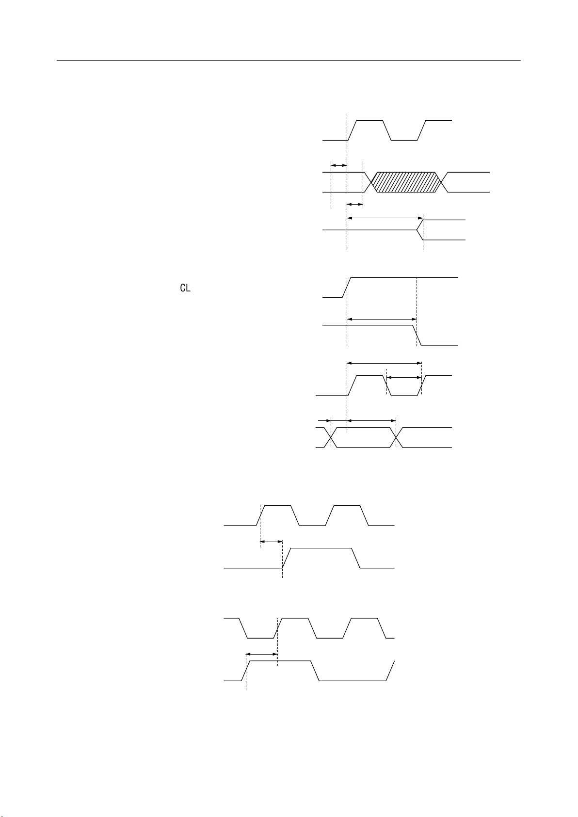
The phase relations between CLKX1 and CLKX2 are shown below.
1. When the CLKX1 pulse rises later than the CLKX2 pulse.
t
L_SCL
valid
CLKX2
Tccd1
CLKX1
2. When the CLKX1 pulse rises earlier than the CLKX2 pulse.
CLKX2
Tccd2
CLKX1
Tccd1: 20.14 [ns]
Tccd2: 3.27 [ns]
10/34

¡ Semiconductor MSM7650
BLOCK FUNCTIONAL DESCRIPTION
Y Limitter
This block limits the contents outside the specified range as follows for input luminance signal
YD specified by the ITU-601 standard.
• Signals are limited to YD = 235 when YD_IN > 235
• Signals are limited to YD = 16 when YD_IN < 16
• In other cases, signals are fed as is to next processing
C Limitter
This block limits the contents outside the specified range as follows for input chrominance
signals specified by the ITU-601 standard.
The input chrominance signal is output as a 2’s complement format.
The processing procedure follows.
1) Format processing for input chrominance signals
• If MR [6] = 0, CD is in offset binary format. CD is converted to 2’s complement format and is
fed to next processing.
• If MR [6] = 1, CD is in 2’s complement format. CD is fed as is to next processing.
2) Clipping processing
• Signals are limited to CD = 112 when CD>112
• Signals are limited to CD = -112 when CD < -112
• In other cases, signals are fed to next processing
In addition, this block separates U and V components from the input chrominance signal CD into
which data of U and V components has been inserted using time sharing, and then passes signals
to the next process.
• Y Level Converter
Converts ITU-601 standard luminance signal level to DAC digital input level.
• U Level Converter
Converts ITU-601 standard chrominance signal level to DAC digital input level.
• V Level Converter
Converts ITU-601 standard chrominance signal level to DAC digital input level.
• YUV Color Generator
This block generates luminance and chrominance signals from over lay color signals OLR,
OLG and OLB. Control signals (CR [2:0] ) control the output content (overlay or color bar) and
output level (100%, 75%, 50%, 25%).
• Overlay Control
This block selects input image data or YUV Color Generator output signals.
It is determined by the level of the control signal (OLC, CR [2]), as shown below:
CR [2] = 1, OLC = ?: Selects color bar signal (YUV Color Generator output signal).
CR [2] = 0, OLC = 1: Selects overlay signal (YUV Color Generator output signal).
CR [2] = 0, OLC = 0: Selects input image data.
11/34
 Loading...