OKI MSM7630GS-BK Datasheet

E2F0005-29-12
¡ Semiconductor
This version: Jan. 1999
Previous version: Mar. 1998
MSM7630¡ Semiconductor
MSM7630
Universal Speech Processor
GENERAL DESCRIPTION
The MSM7630 is a speech processor LSI device with internal D/A converter. It is optimized for
speech output applications such as text-to-speech conversion.
FEATURES
• Parallel and serial interfaces
• Single 3.3V power supply
• 5V interface available
• Internal 16-bit x 16-bit to 32-bit multiplier (2-clock data throughput)
• 26 VAX MIPS performance at 40 MHz operation (when using ordinary ROM/SRAM)
• Package: 100-pin plastic QFP (QFP100-P-1420-0.65-BK)(Product name: MSM7630GS-BK)
1/95
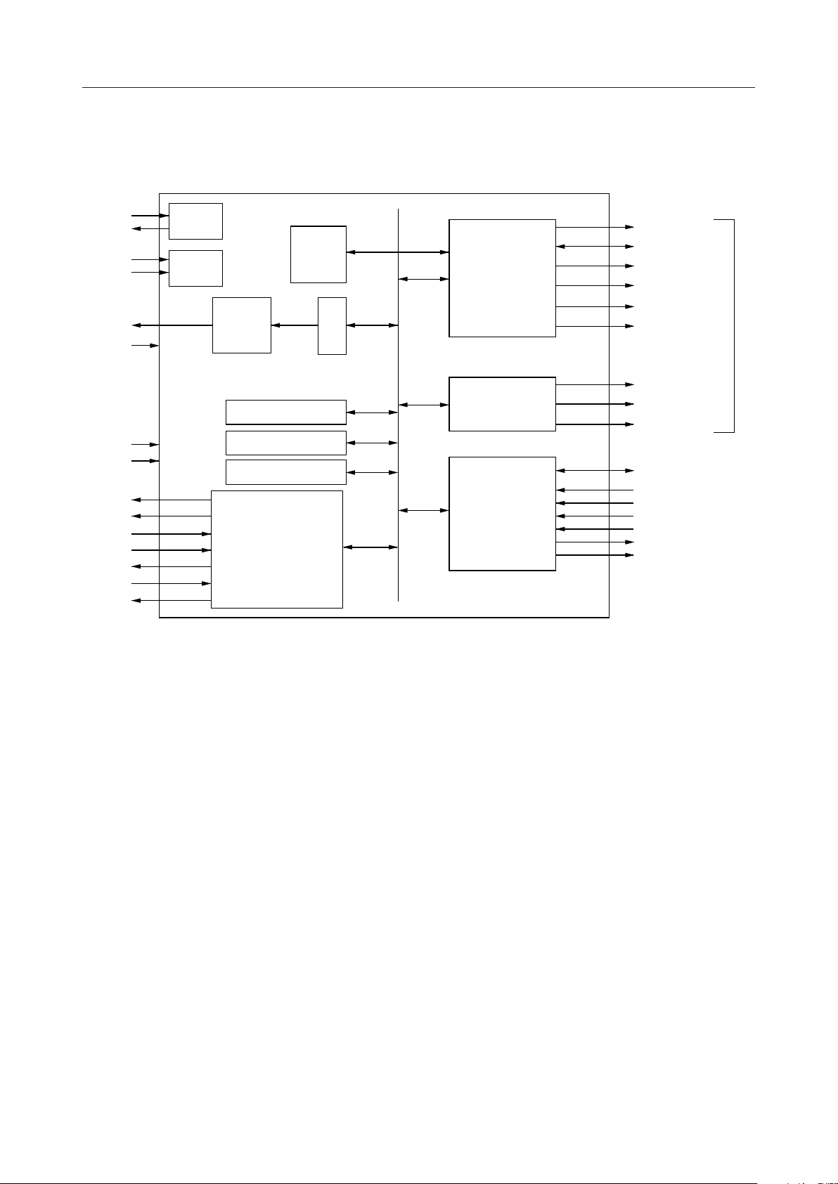
BLOCK DIAGRAM
MSM7630¡ Semiconductor
CLK
MCLKA
TSTM
EXINT
DAO1
SG
RST
STBY
SCLK
TXD
RXD
DSR
DTR
CTS
RTS
PLL
TST
DAC
TMR
TMR
TMR
SIO
MPY
REG
CPU
DRAMC
PIO
A23-0
D31-16
WR0,1
RD
ROM
SRAM
Local Bus
RAS
CAS0,1
WE
PD7-0
PSTB
PACK
PCS
PIOA
POBF
PIBF
2/95

PIN CONFIGURATION (TOP VIEW)
DAO1
TEST0SGVDDVDDGND
99989796959493929190898887868584838281
100
GNDXOCLK
CLKA
UPORT
TSTM2
TSTM1
VDDEXTINT
A23
A22
A21
A20
MSM7630¡ Semiconductor
A19
GND
GND
RST
RD
STBY
WR1
WR0
AS
ROM
V
DD
SRAM
D31
D30
D29
D28
D27
GND
D26
D25
D24
D23
D22
D21
V
DD
D20
D19
D18
D17
D16
PD7
10
11
12
13
14
15
16
17
18
19
20
21
22
23
24
25
26
27
28
29
30
80
79
78
77
76
75
74
73
72
71
70
69
68
67
66
65
64
63
62
61
60
59
58
57
56
55
54
53
52
51
A18
GND
A17
A16
A15
A14
A13
A12
V
DD
A11
A10
A9
A8
A7
A6
A5
GND
A4
A3
A2
A1
A0
CAS1
CAS0
V
DD
WE
SCLK
RXD
RAS
TXD
1
2
3
4
5
6
7
8
9
31323334353637383940414243444546474849
PD6
GND
PD5
PD4
PD3
PD2
PD1
PD0
PIOA
V
PCS
PACK
PIBF
PSTB
POBF
DSR
RTS
GND
CTS
DD
100-Pin Plastic QFP
50
DTR
3/95

PIN DESCRIPTIONS
MSM7630¡ Semiconductor
Symbol
D31-16
A23-0
ROM
SRAM
RD
WR0,1
WE
AS
TXD
RXD
DTR
DSR
RTS
CTS
SCLK
PD7-0
PACK
PSTB
PCS
PIOA
POBF
PIBF
UPORT
TEST0
DAO1
SG
CLK
XO
CLKA
RST
STBY
EXTINT
TSTM2,1
Type
I/O
O
O
O
O
O
ORAS
OCAS0,1
O
O
O
I
O
I
O
I
O
I/O
I
I
I
I
3-state
3-state
O
I
O
I
I
O
O
I
I
I
I
Description
16-bit data bus. 8-bit devices are accessed through D31-24.
24-bit address bus. DRAM addresses are output from A13-0.
ROM select signal. ROM indicates that ROM space is assigned to the specified address.
It is used as a chip select signal.
SRAM select signal. SRAM indicates that SRAM space is assigned to the specified address.
It is used as a chip select signal.
Read signal. RD is active during both 8-bit and 16-bit reads.
Write signals. WR0 corresponds to writes from D31-24, and WR1 corresponds to
writes from D23-16.
Row address strobe. RAS is active during both 8-bit and 16-bit reads.
Column address strobe. CAS0 corresponds to accesses from D31-24, and CAS1
corresponds to accesses from D23-16.
Write enable. WE is active during writes to DRAM space as the DRAM write signal.
Address strobe.
Serial data output.
Serial data input.
Control signal indicating SIO can transmit and receive.
Input signal indicating that modem is in operable state.
SIO transmit request signal.
Input signal indicating that modem can transmit.
Synchronous transfer clock output.
Parallel port data input/output.
Parallel port read signal. Set high for Centronics interface.
Parallel port write signal. Strobe signal for Centronics interface.
Parallel port chip select signal.
Parallel port address signal. Selects data or status during an access.
Output port buffer full. Indicates that data has been set in the output buffer.
Input port buffer full. Indicates that there is data in the input buffer.
Busy output signal for Centronics interface.
General flag output signal.
Connects with SG.
D/A converter output.
Signal ground. Connects with TEST0.
Clock input signal.
Clock signal. Inverse of CLK.
Internal clock signal.
Reset input.
Standby signal. STBY suspends operation and places the MSM7630 in a standby state.
External interrupt signal.
Test mode select input signal.
4/95

ABSOLUTE MAXIMUM RATINGS
MSM7630¡ Semiconductor
Parameter Symbol Condition
Power Supply Voltage V
Input Voltage V
Storage Temperature T
DD
IN
STG
Ta = 25°C
(excluding TEST0)
Ta = 25°C
—
RECOMMENDED OPERATING CONDITIONS
Parameter Symbol Conditon
Power Supply Voltage V
Operating Temperature T
DD
op
—
—
ELECTRICAL CHARACTERISTICS
DC Characteristics
Parameter Symbol Condition
"H" Input Voltage V
"L" Input Voltage V
"H" Input Voltage V
"L" Input Voltage V
"H" Output Voltage V
"L" Output Voltage V
Input Leakage Current I
Output Leakage Current I
Dynamic Supply Current I
Static Supply Current I
D/A Output Relative Accuracy V
D/A Output Impedance R
IH
IL
IH
IL
OH
OL
LI
LO
DO
DS
DAE
DA
Excluding CLK
Excluding CLK
CLK
CLK
= –4 mA
I
OH
I
= 4 mA
OL
0 £ V
0 £ V
f
V
DD
OPE
£ V
IN
DD
£ V
OUT
= 3.6 V,
= 20 MHz
—
No load
—
DD
Rating
–0.3 to +4.5
–0.3 to +5.5 V
–55 to +125 °C
Range
3.0 to 3.6
–40 to +85 °C
= 3.0 to 3.6 V, Ta = –40 to +85°C)
(V
DD
Min. Typ. Max.
2.2
—
0.8 ¥ V
—
2.4
—
–10
–10
—
—
—
12
DD
—
—
—
—
—
—
—
—
—
—
—
20
0.2 ¥ V
Unit
V
Unit
V
Unit
—
V
0.8 V
—V
DD
V
—V
0.4 V
+10 mA
+10 mA
120 mA
1.5 mA
10 mV
28 kW
5/95

AC Characteristics
MSM7630¡ Semiconductor
Parameter Symbol Condition
Source Oscillation Period t
Input Clock Low-Level
t
W_CLKL
Minimum Width
Input Clock High-Level
t
W_CLKH
Minimum Width
Operating Period t
CLKA Delay Time t
XO Delay Time t
Required RST Time t
W_RST
A Delay Time t
D Setup Time t
D Hold Time t
D Delay Time t
RD Delay Time t
WR Delay Time t
UPORT Delay Time t
EXINT Setup Time t
UPORT
S_EXINT
OSC
CYC
CLK
XO
A
S_D
H_D
D
RD
WR
—
—
—
—
—
—
—
—
—
—
—
—
Falling
Rising
—
—
(VDD = 3.0 to 3.6 V, T
= –40 to +85°C)
OPE
Min. Typ. Max.
25
13
8
25
—
—
1024
—
2
6
—
—
—
—
—
2
—
—
—
—
—
—
—
—
—
—
—
—
—
—
—
—
50
—ns
—ns
50 ns
12 ns
7ns
—t
22 ns
—ns
—ns
25 ns
20 ns
22 ns
22 + 0.5 t
20 ns
—ns
CYC
Unit
ns
CYC
ns
6/95

ROM, SRAM Access
Parameter Symbol Condition
RD Pulse Width t
WR Pulse Width t
A to RD Time t
A to WR Time t
WR to SRAM Time t
ROM Delay Time t
SRAM Delay Time t
ROM Pulse Width t
SRAM Pulse Width t
WR to D Time t
W_RD
W_WR
W_ARD
W_AWR
W_WRSRAM
ROM
SRAM
W_ROM
W_SRAM
W_WRD
ROM, SRAM
3t to 12t Access
SRAM
3t to 12t Access
ROM, SRAM
3t, 4t Access
ROM, SRAM
5t to 12t Access
SRAM
3t to 12t Access
SRAM
3t to 12t Access
—
—
ROM
3t to 12t Access
SRAM
3t to 12t Access
SRAM
3t Access
SRAM
4t to 12t Access
(V
= 3.0 to 3.6 V, T
DD
= –40 to +85°C)
OPE
Min. Typ. Max.
2
1.5
—
—
—
—
—
—
3
3
—
—
—
—
—
—
—
—
11 t
10.5 t
1
2
1
1
—t
—t
—t
—t
20 + 0.5 t
20 + 0.5 t
12 t
12 t
0
1
—t
—t
MSM7630¡ Semiconductor
CYC
CYC
Unit
CYC
CYC
CYC
CYC
CYC
CYC
ns
ns
CYC
CYC
CYC
CYC
7/95

DRAM Access
Parameter Symbol Condition
RAS Delay Time t
RAS Pulse Width t
A to RAS Time t
CAS Delay Time t
CAS Pulse Width t
A to CAS Time t
RAS to CAS Time t
WE to CAS Time t
WE Delay Time t
WE Pulse Width t
A to WE Time t
Required Precharge Time t
CAS to RAS Time t
CAS to D Time t
RAS
W_RAS
W_ARAS
CAS
W_CAS
W_ACAS
W_RASCAS
W_WECAS
WE
W_WE
W_AWE
W_PREC
W_CASRAS
W_EDO
—
—
—
2nt access falling
edge
Normal
Normal
Refresh
—
—
—
—
—
—
—
—
Hyper Mode
(V
= 3.0 to 3.6 V, T
DD
= –40 to +85°C)
OPE
Min. Typ. Max.
—
3
1
—
—
1.5
4
0.5
1.5
1.5
—
3
—
1
—
—
—
—
—
—
—
—
—
—
—
—
—
—
—
—
18 ns
Note 1 t
—t
18 + 0.5 t
18 ns
2t
5t
1ns
2t
2t
20 ns
Note 1 t
1
—t
Note 2 t
1
—t
1t
MSM7630¡ Semiconductor
CYC
Unit
CYC
CYC
ns
CYC
CYC
CYC
CYC
CYC
CYC
CYC
CYC
CYC
General Device Access
Parameter Symbol Condition
AS Delay Time t
AS
—
= 3.0 to 3.6 V, T
(V
DD
= –40 to +85°C)
OPE
Min. Typ. Max.
—
—
18 ns
Unit
8/95

When DS bit = 0
MSM7630¡ Semiconductor
Parameter Symbol Condition
AS Pulse Width t
A to AS Time t
RD Pulse Width t
A to RD Time t
WR Pulse Width t
A to WR Time t
D to WR Time t
W_AS
W_AAS
W_RD
W_ARD
W_WR
W_AWR
W_DWR
4t to 7t Access
(X bit = 0)
8t to 14t Access
(X bit = 1)
4t to 7t Access
(X bit = 0)
8t to 14t Access
(X bit = 1)
4t to 7t Access
(X bit = 0)
8t to 14t Access
(X bit = 1)
4t to 7t Access
(X bit = 0)
8t to 14t Access
(X bit = 1)
4t to 7t Access
(X bit = 0)
8t to 14t Access
(X bit = 1)
4t to 7t Access
(X bit = 0)
8t to 14t Access
(X bit = 1)
4t to 7t Access
(X bit = 0)
8t to 14t Access
(X bit = 1)
= 3.0 to 3.6 V, T
(V
DD
= –40 to +85°C)
OPE
Min. Typ. Max.
2
6
—
—
2
6
—
—
2
6
—
—
—
—
—
—
—
—
—
—
5t
12 t
1
1
—t
—t
5t
12 t
1
1
—t
—t
5t
12 t
1
1
0
0
—t
—t
—t
—t
Unit
CYC
CYC
CYC
CYC
CYC
CYC
CYC
CYC
CYC
CYC
CYC
CYC
CYC
CYC
9/95

When DS bit = 1
Parameter Symbol Condition
AS Pulse Width
Note 3
A to AS Time t
RD Pulse Width t
A to RD Time t
WR Pulse Width t
A to WR Time t
D to WR Time t
t
W_AS
W_AAS
W_RD
W_ARD
W_WR
W_AWR
W_DWR
4t to 7t Access
(X bit = 0)
8t to 14t Access
(X bit = 1)
4t to 7t Access
(X bit = 0)
8t to 14t Access
(X bit = 1)
4t to 7t Access
(X bit = 0)
8t to 14t Access
(X bit = 1)
4t to 7t Access
(X bit = 0)
8t to 14t Access
(X bit = 1)
4t to 7t Access
(X bit = 0)
8t to 14t Access
(X bit = 1)
4t to 7t Access
(X bit = 0)
8t to 14t Access
(X bit = 1)
4t to 7t Access
(X bit = 0)
8t to 14t Access
(X bit = 1)
(V
= 3.0 to 3.6 V, T
DD
= –40 to +85°C)
OPE
Min. Typ. Max.
2
6
—
—
2
6
—
—
2
6
—
—
—
—
—
—
—
—
—
—
5t
12 t
1
1
—t
—t
5t
12 t
1
1
—t
—t
5t
12 t
2
3
1
2
—t
—t
—t
—t
MSM7630¡ Semiconductor
Unit
CYC
CYC
CYC
CYC
CYC
CYC
CYC
CYC
CYC
CYC
CYC
CYC
CYC
CYC
10/95

Serial Interface
MSM7630¡ Semiconductor
Parameter Symbol Condition
RTS Delay Time t
Required RXD Time t
RXD Setup Time t
RXD Hold Time t
CTS Setup Time t
CTS Hold Time t
TXD Delay Time t
TXD Pulse Width t
DTR Delay Time t
SCLK Delay Time t
SCLK Pulse Width t
Parallel Interface
Parameter Symbol Condition
PACK to PD Delay Time t
PACK to PD Hi Z Delay Time t
PCS Setup Time for PSTB/PACK
PCS Hold Time for PSTB/PACK t
PIOA Setup Time for PSTB/PACK
PIOA Hold Time for PSTB/PACK t
Required PACK Time t
Required PSTB Time t
PD Setup Time for PSTB t
PD Hold Time for PSTB t
RTS
W_RXD
S_RXD
H_RXD
S_CTS
H_CTS
TXD
W_TXD
DTR
SCLK
W_SCLK
PACK
PRDZ
t
S_PCS
H_PCS
t
S_PIOA
H_PIOA
W_PACK
W_PSTB
S_PD
H_PD
—
—
—
—
—
—
—
—
—
—
—
—
—
—
—
—
—
—
—
—
—
= 3.0 to 3.6 V, T
(V
DD
Min. Typ. Max.
—
1/bps
0.5/bps
0.5/bps
0
0
—
1/bps
—
—
1/bps
(V
DD
—
—
—
—
—
—
—
—
—
—
—
= 3.0 to 3.6 V, T
Min. Typ. Max.
—
—
0
0
0
3
30 + t
30 + 2 t
–t
CYC
8
CYC
CYC
—
—
—
—
—
—
—
—
—
—
= –40 to +85°C)
OPE
Unit
20 ns
—s
—
—
—
—
s
s
ns
ns
20 ns
—s
20 ns
20 ns
—s
= –40 to +85°C)
OPE
Unit
22 ns
22 ns
—ns
—ns
—ns
—ns
—ns
—ns
—ns
—ns
Note 1 According to DRAM configuration
Note 2 By the DRAM access timing
Note 3 In the case of writing, increased by 1 clock when X bit = 0 and by 2 clocks when X bit
= 1.
Note 4 Flash memory access timing is the same with the SRAM timing.
11/95

TIMING DIAGRAM
Clock And Reset
t
OSC
CLK
XO
CLKA
RST
t
XO
t
CLKA
t
W_CLKLtW_CLKH
t
W_RST
t
MSM7630¡ Semiconductor
CYC
12/95
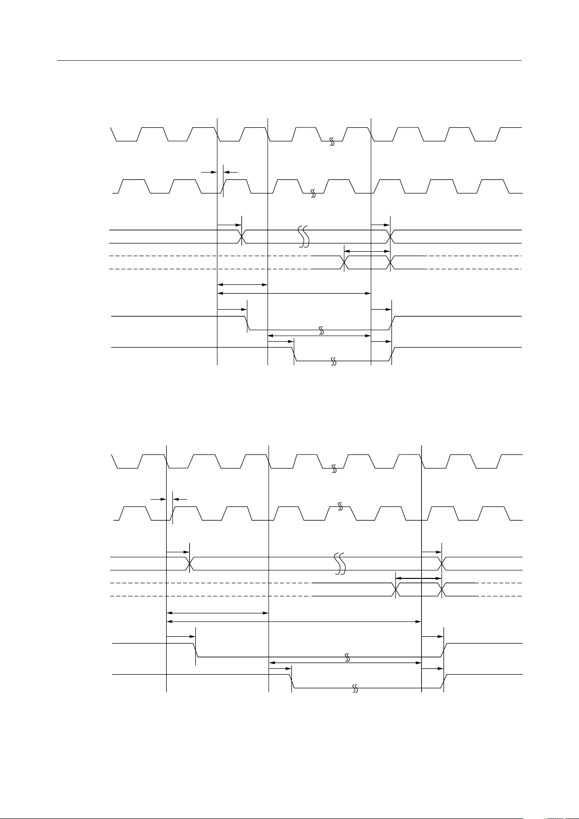
ROM Read
CLK
CLKA
t
CLKA
MSM7630¡ Semiconductor
ROM
RD
CLK
CLKA
t
A
A
t
S_D
D
t
t
CLKA
t
ROM
W_ARD
t
RD
tt
3
t/4
tt
tt
t Access
tt
t
W_ROM
t
W_RD
t
A
t
H_D
t
ROM
t
RD
ROM
RD
t
A
A
t
S_D
D
t
t
ROM
W_ARD
5
tt
t/6
tt
t
tt
t/8
tt
RD
tt
t/10
tt
t
W_ROM
tt
t/12
tt
tt
t Access
tt
t
W_RD
t
A
t
H_D
t
ROM
t
RD
13/95
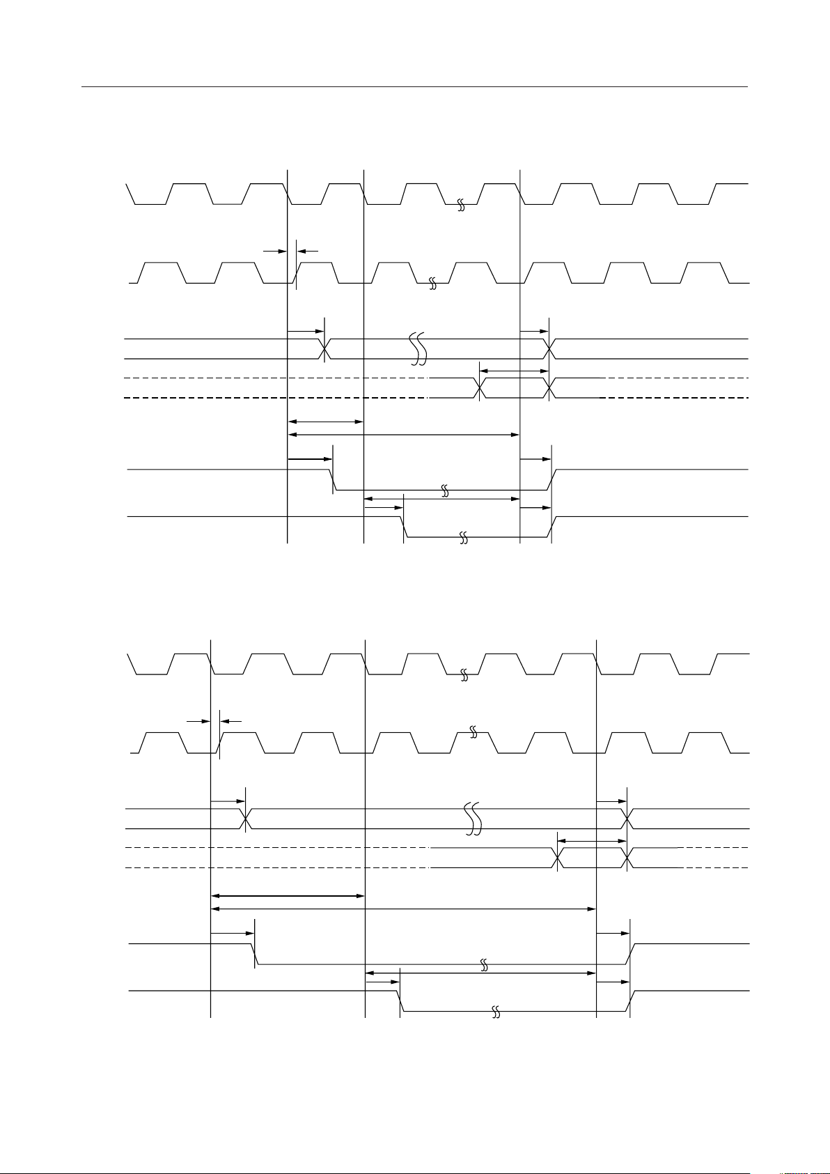
SRAM Read
CLK
CLKA
t
CLKA
MSM7630¡ Semiconductor
SRAM
RD
CLK
CLKA
t
A
t
A
A
t
S_D
t
H_D
D
t
t
CLKA
t
SRAM
W_ARD
t
W_SRAM
t
SRAM
t
RD
tt
tt
3
t/4
t Access
tt
tt
t
W_RD
t
RD
SRAM
RD
t
A
t
A
A
t
S_D
t
H_D
D
t
t
SRAM
W_ARD
5
tt
t/6
tt
t
RD
tt
t/8
tt
t
W_SRAM
tt
t/10
tt
tt
t/12
tt
t
W_RD
tt
t Access
tt
t
SRAM
t
RD
14/95
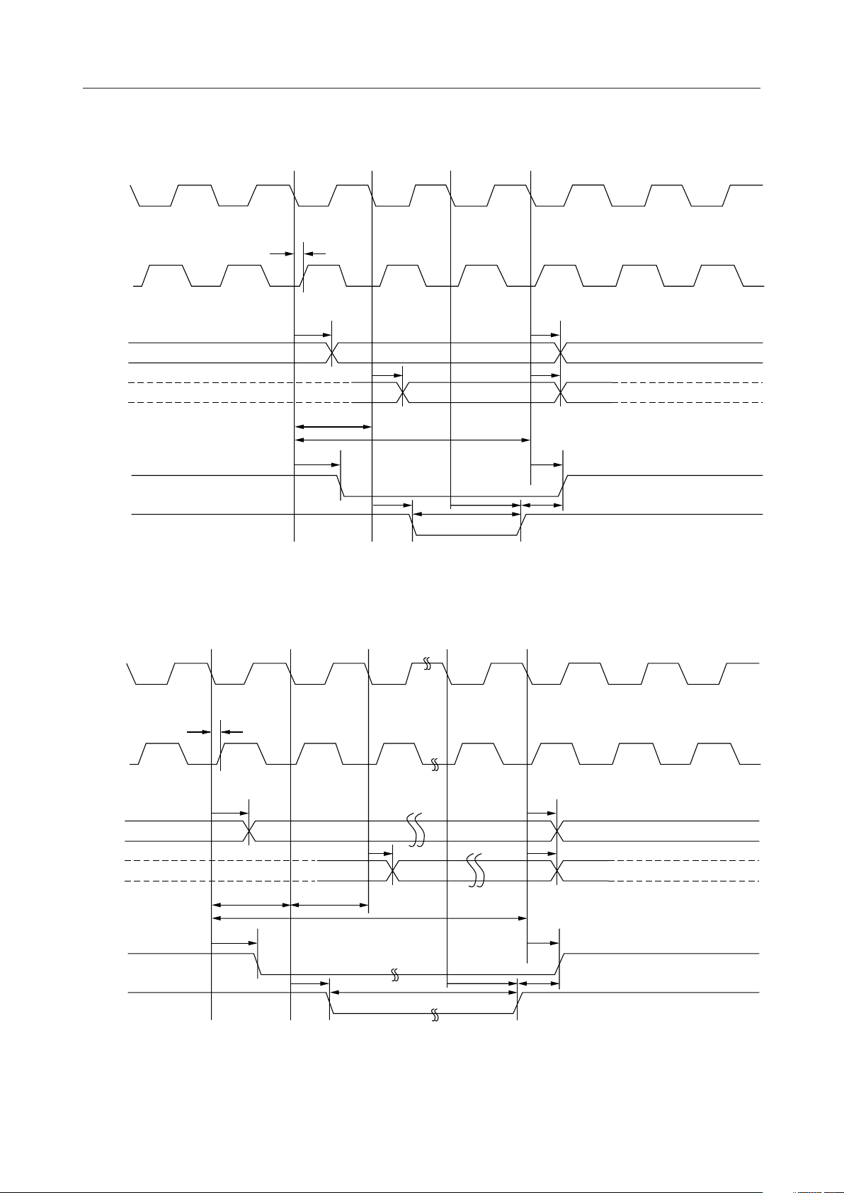
SRAM Write
CLK
CLKA
t
CLKA
MSM7630¡ Semiconductor
SRAM
WR
CLK
CLKA
t
A
t
A
A
t
D
t
D
D
t
t
CLKA
t
SRAM
W_AWR
t
WR
t
W_SRAM
t
tt
3
t Access
tt
WR
t
W_WR
t
SRAM
t
W_WRSRAM
SRAM
WR
t
A
t
A
A
t
D
t
D
D
t
SRAM
t
W_AWR
t
WR
t
W_WRD
tt
4
t/5
tt
tt
t/6
tt
tt
t/8
tt
t
W_SRAM
t
W_WR
tt
t/10
tt
t
WR
tt
t/12
tt
tt
t Access
tt
t
SRAM
t
W_WRSRAM
15/95
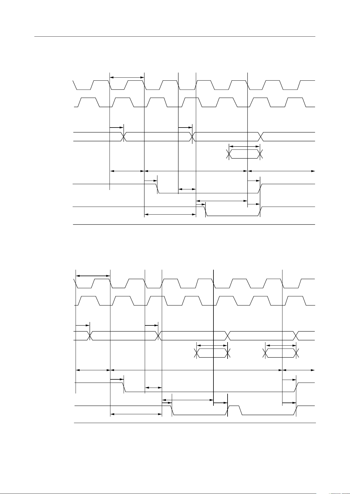
DRAM Read
CLK
CLKA
t
OSC
MSM7630¡ Semiconductor
RAS
CAS
WE
CLK
t
A
A
row address column address
t
A
t
S_D
t
H_D
D
t
OSC
t
W_ARAS
t
RAS
t
W_RASCAS
tt
2n
t Access (Fast Page Mode)
tt
t
CAS
t
W_RAS
t
W_ACAS
t
W_CAS
t
RAS
t
CAS
t
W_PREC
CLKA
RAS
CAS
WE
t
A
A
row address column address
t
A
column address
t
S_D
t
H_D
t
S_D
t
H_D
D
t
W_ARAS
t
RAS
t
W_ACAS
t
CAS
t
W_RASCAS
tt
2n
t Access (Fast Page Mode)
tt
t
t
W_CAS
W_RAS
t
CAS
t
t
RAS
W_PREC
t
CAS
16/95
CLK
CLKA
t
OSC
MSM7630¡ Semiconductor
CLK
RAS
CAS
WE
t
A
A
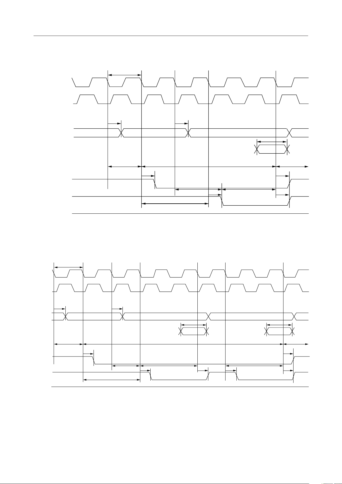
row address
t
A
column address
t
S_D
t
H_D
D
t
OSC
t
W_ARAS
t
RAS
t
W_RASCAS
tt
3n
t Access (Fast Page Mode)
tt
t
W_ACAS
t
CAS
t
W_RAS
t
W_CAS
t
W_PREC
t
RAS
t
CAS
CLKA
RAS
CAS
WE
t
A
A
D
t
W_ARAS
t
RAS
t
t
W_RASCAS
A
column addressrow address
t
S_D
t
W_RAS
t
W_ACAS
t
CAS
tt
3n
t Access (Fast Page Mode)
tt
t
W_CAS
t
t
CAS
H_D
column address
t
S_D
t
W_CAS
t
CAS
t
W_PREC
t
RAS
t
t
H_D
CAS
17/95
CLK
CLKA
t
MSM7630¡ Semiconductor
OSC
RAS
CAS
WE
CLK
t
A
A
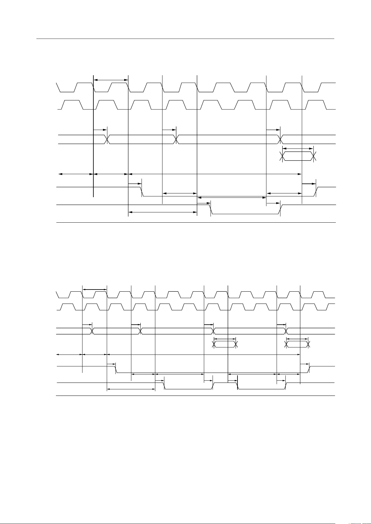
row address
t
A
t
A
column address
t
S_D
t
H_D
D
t
OSC
t
W_ARAS
t
W_RAS
t
RAS
t
W_ACAS
t
t
W_RASCAS
tt
3n
t Access (Hyperpage Mode)
tt
CAS
t
W_CAS
t
W_EDO
t
CAS
t
RAS
t
W_PREC
CLKA
RAS
CAS
WE
t
A
A
D
t
W_PREC
t
W_ARAS
t
RAS
t
t
W_RASCAS
3n
A
t
A
column addressrow address
t
S_D
t
W_RAS
t
W_ACAS
t
CAS
tt
t Access (Hyperpage Mode)
tt
t
W_CAS
t
CAS
column address
t
H_D
t
W_CAS
t
CAS
t
t
S_D
t
A
W_EDO
t
CAS
t
RAS
t
H_D
18/95
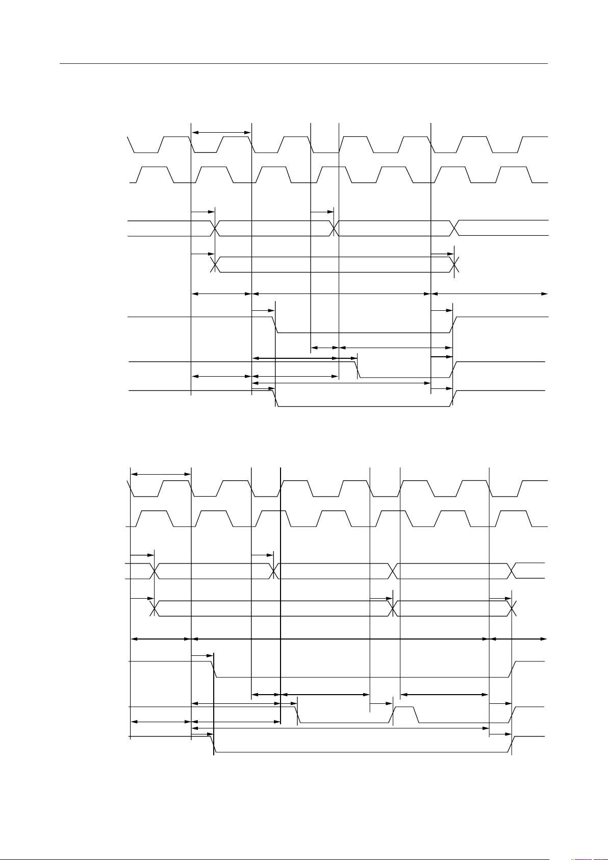
DRAM Write
CLK
CLKA
t
MSM7630¡ Semiconductor
OSC
RAS
CAS
WE
CLK
t
A
A
t
D
row address column address
t
A
t
D
D
t
OSC
t
W_ARAS
t
RAS
t
t
W_WECAS
WE
W_ACAS
t
W_RASCAS
t
W_AWE
t
tt
2n
t Access (Fast Page Mode)
tt
t
W_RAS
t
W_WE
t
CAS
t
W_CAS
t
RAS
t
WE
t
CAS
t
W_PREC
CLKA
RAS
CAS
WE
t
A
A
t
D
row address
t
A
column address column address
t
D
t
D
D
t
CAS
t
t
W_CAS
W_RAS
t
W_WE
t
CAS
t
W_CAS
t
CAS
t
WE
t
W_PREC
t
W_ARAS
t
W_AWE
t
RAS
t
W_RASCAS
t
W_ACAS
t
W_WECAS
t
WE
tt
2n
t Access (Fast Page Mode)
tt
19/95
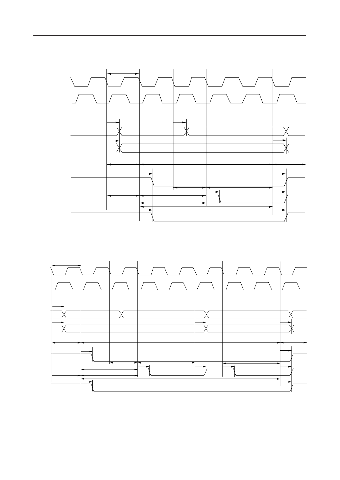
CLK
CLKA
t
MSM7630¡ Semiconductor
OSC
CLK
RAS
CAS
WE
D
A
t
OSC
t
A
t
A
row address column address
t
D
t
W_ARAS
t
RAS
t
W_ACAS
t
W_AWE
tt
3n
t Access (Fast Page Mode/Hyperpage Mode)
tt
t
W_RASCAS
t
W_WECAS
t
WE
t
W_RAS
t
CAS
t
W_CAS
t
W_PREC
t
RAS
t
t
CAS
t
D
WE
CLKA
RAS
CAS
WE
t
A
A
t
D
D
t
W_ARAS
t
W_AWE
row address
t
RAS
t
W_RASCAS
t
W_CAS
t
WE
3n
t Access (Fast Page Mode/Hyperpage Mode)
t
W_ACAS
tt
tt
column address column address
t
D
t
W_RAS
t
CAS
t
W_CAS
t
W_WE
t
CAS
t
CAS
t
W_CAS
t
CAS
t
t
t
RAS
WE
t
D
W_PREC
20/95
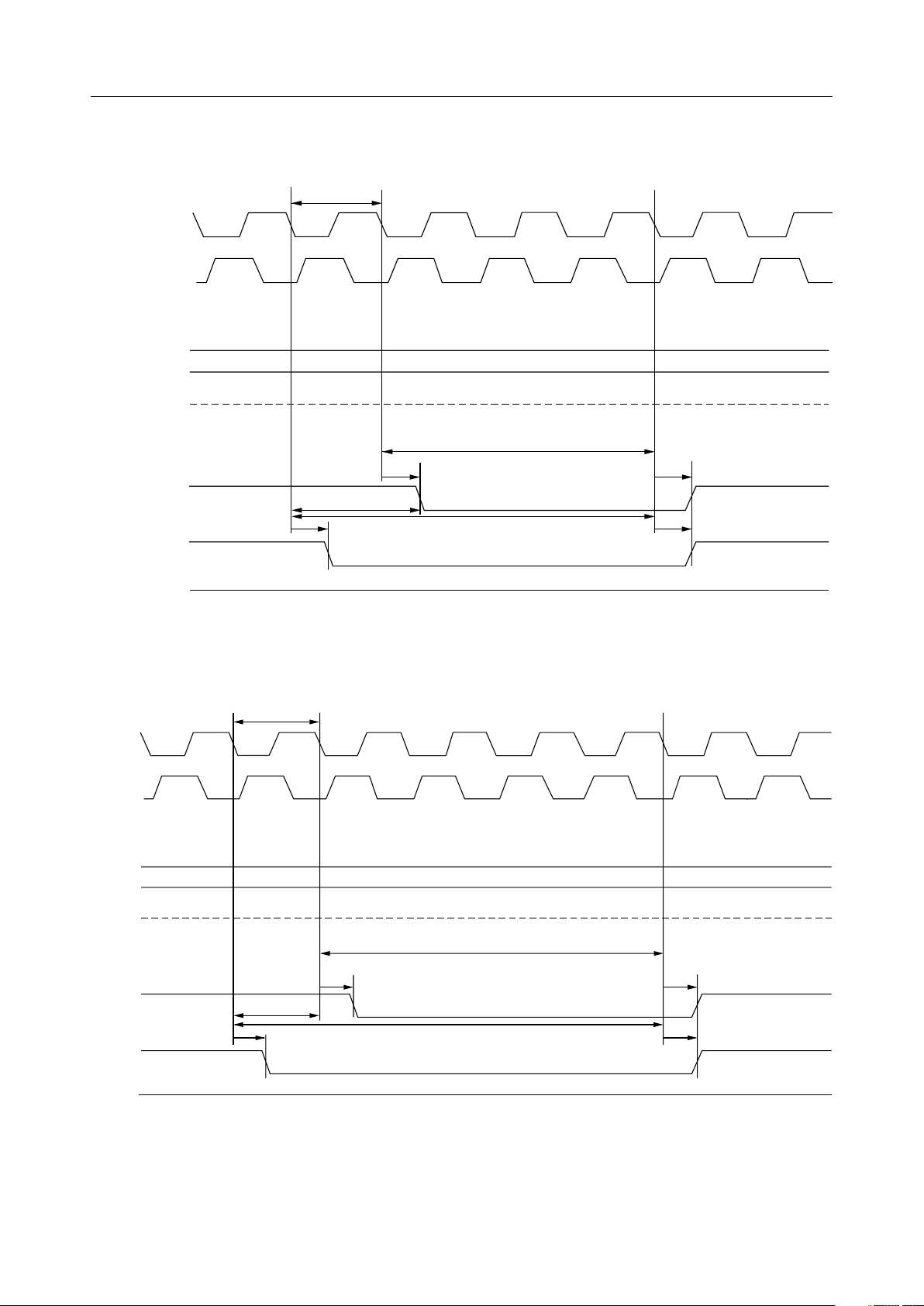
DRAM Refresh
CLK
CLKA
t
OSC
MSM7630¡ Semiconductor
CLK
CLKA
RAS
CAS
WE
A
D
t
RAS
t
W_CASRAS
t
CAS
tt
2n
t CAS-Before-RAS Refresh
tt
t
OSC
ignore
ignore
t
W_RAS
t
W_CAS
t
RAS
t
CAS
RAS
CAS
WE
A
D
t
RAS
t
W_CASRAS
t
CAS
tt
3n
t CAS-Before-RAS Refresh
tt
ignore
ignore
t
W_RAS
t
W_CAS
t
RAS
t
CAS
21/95
CLK
CLKA
t
OSC
MSM7630¡ Semiconductor
RAS
CAS
WE
A
D
t
RAS
t
W_CASRAS
t
CAS
ignore
ignore
t
W_RAS
t
W_CAS
t
RAS
t
CAS
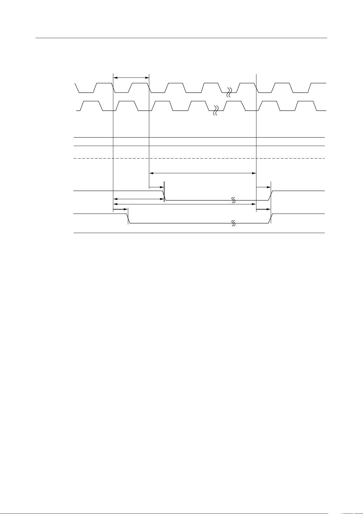
CAS-Before-RAS Self-Refresh
22/95
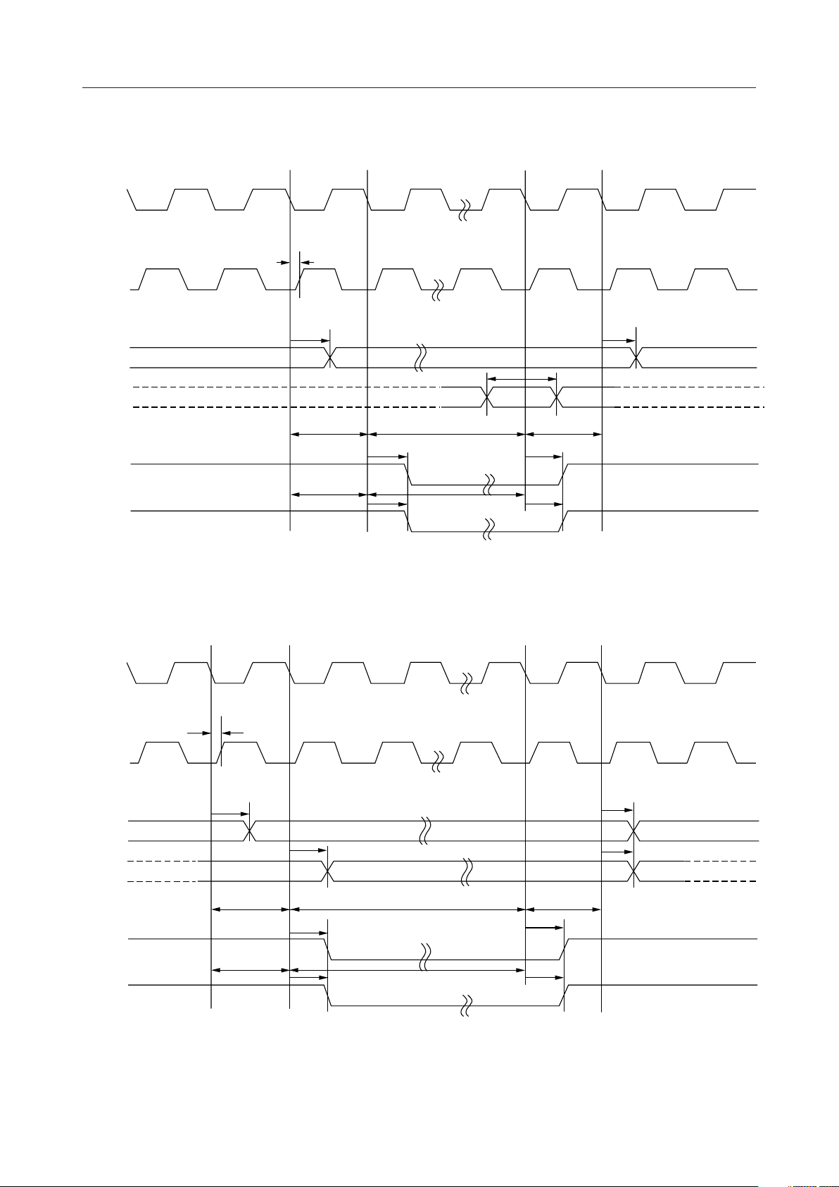
General Device Access
CLK
CLKA
t
CLKA
MSM7630¡ Semiconductor
AS
RD
CLK
CLKA
t
A
t
A
A
t
S_D
t
H_D
D
t
W_AAS
t
W_ARD
t
W_AS
t
AS
t
W_RD
t
RD
t
t
AS
W_AAS
t
RD
Bus Read
t
CLKA
AS
WR
t
t
A
A
A
t
D
t
D
D
t
W_WR
t
W_AS
t
W_AAS
t
t
AS
WR
t
W_AAS
t
W_AWR
t
AS
t
WR
Bus Write (When DS bit in the SCR register is "0")
23/95
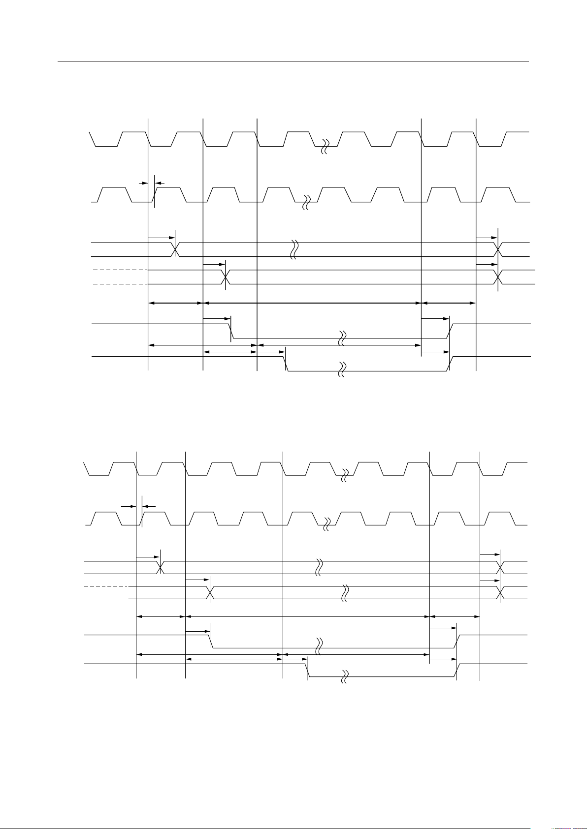
CLK
CLKA
t
CLKA
MSM7630¡ Semiconductor
WR
CLK
CLKA
AS
t
A
t
A
A
t
D
t
D
D
t
W_AAS
t
W_AWR
t
AS
t
W_DWR
t
W_AS
t
W_WR
t
WR
t
W_AAS
t
AS
t
WR
Bus Write (When DS bit is "1" and X bit is "0" in the SCR register)
t
CLKA
AS
WR
t
t
A
A
A
t
D
t
D
D
t
W_AAS
t
W_AWR
t
AS
t
W_DWR
t
W_AS
t
WR
t
W_WR
t
W_AAS
t
AS
t
WR
Bus Write (When DS bit is "1" and X bit is "1" in the SCR register)
24/95
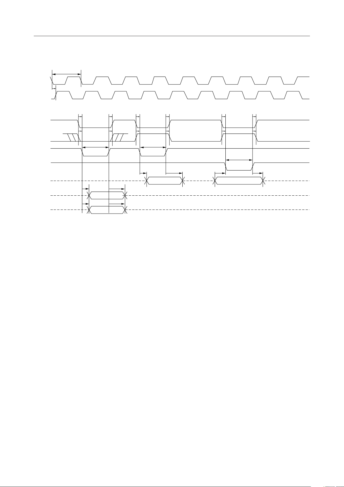
Parallel Interface
t
OSC
CLK
t
CLKA
CLKA
MSM7630¡ Semiconductor
PCS
PIOA
PACK
PSTB
PD
PIBF
POBF
t
S_PCS
t
S_PIOA
t
W_PACK
t
PACK
t
PACK
t
H_PCS
t
H_PIOA
t
PACK
t
PRDZ
t
PRDZ
t
S_PCS
t
S_PIOA
t
W_PACK
t
PRDZ
t
H_PCS
t
H_PIOA
t
S_PD
t
S_PCS
t
S_PIOA
t
W_PSTB
t
H_PCS
t
H_PIOA
t
H_PD
25/95
MSM7630¡ Semiconductor
26/95
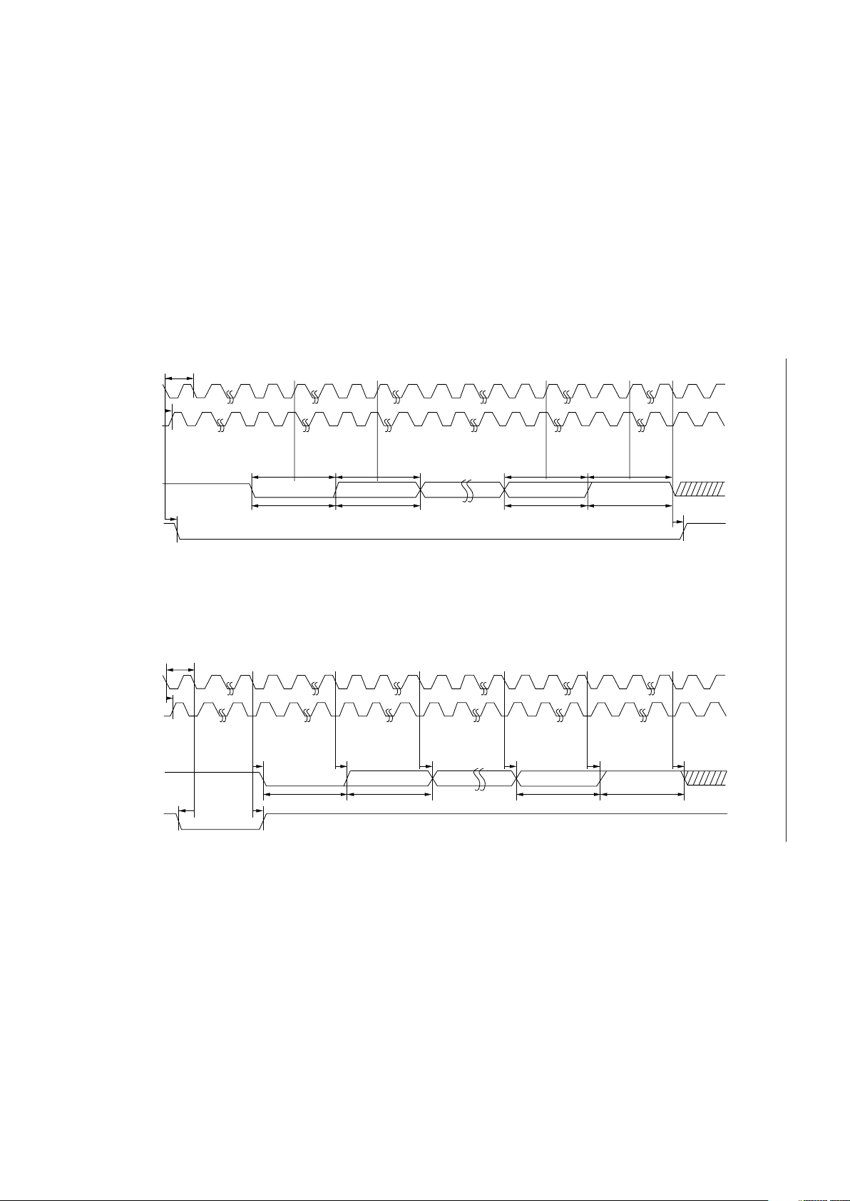
Serial Interface
CLK
CLKA
RXD
RTS
t
OSC
t
CLKA
t
RTS
t
H_RXD
t
S_RXD
t
W_RXD
t
W_RXD
bit 7 Stop_bit (= 1)
t
H_RXD
t
S_RXD
bit 6bit 1bit 0Start_bit (= 0)
t
H_RXD
t
S_RXD
t
H_RXD
t
S_RXD
t
W_RXD
t
W_RXD
t
RTS
bit 6bit 1
bit 0
Stop_bit (= 1)bit 7
Start_bit (= 0)
t
TXD
t
TXD
t
TXD
t
TXD
t
TXD
t
TXD
t
W_TXD
t
W_TXD
t
W_TXD
t
W_TXD
t
H_CTS
t
S_CTS
t
OSC
t
CLKA
CLK
CLKA
TXD
CTS
CLK
CLKA
t
CLKA
MSM7630¡ Semiconductor
t
SCLK
SCLK
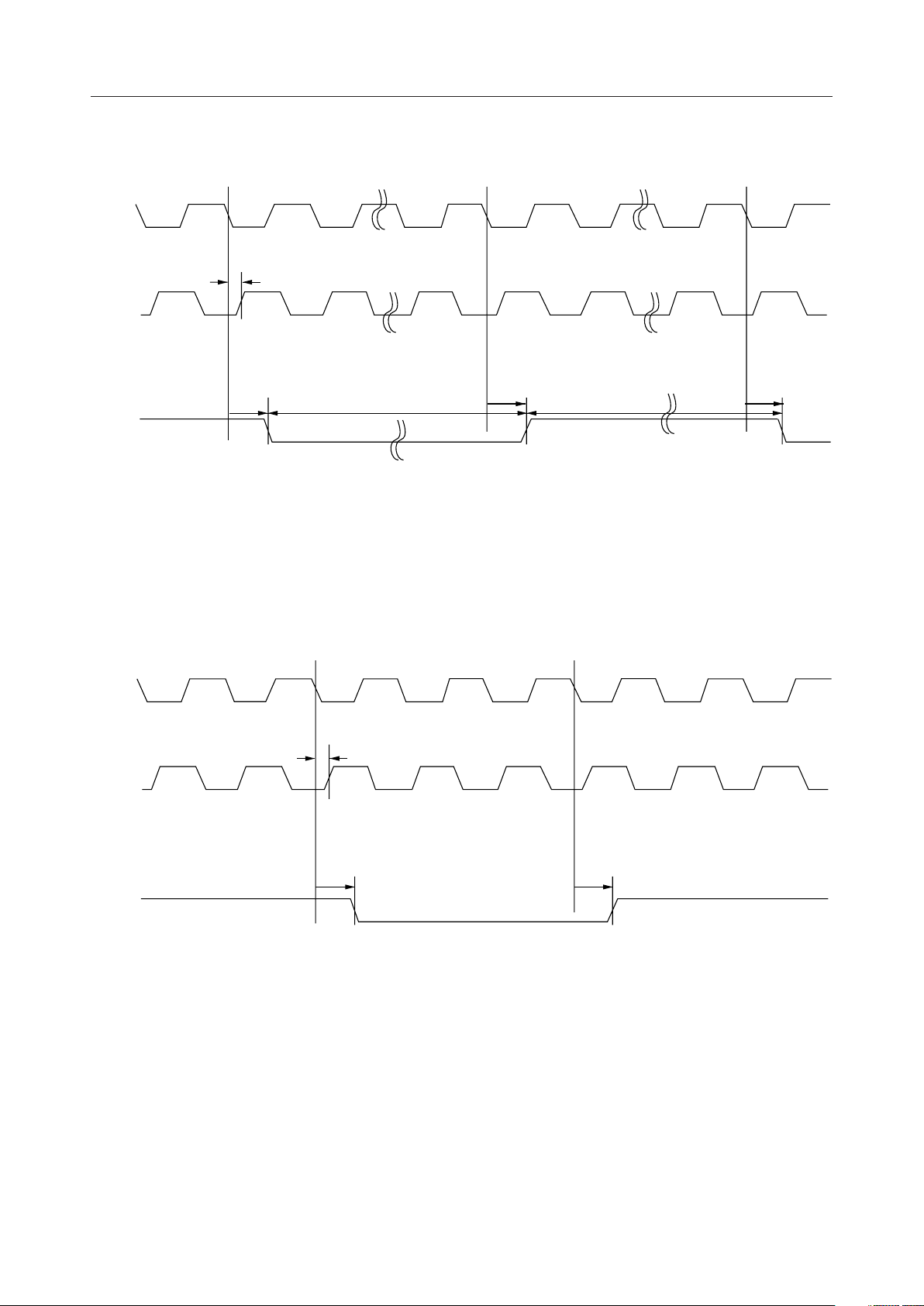
General Port Output
CLK
CLKA
t
t
W_SCLK
SCLK
Synchronous Transfer Output
t
CLKA
t
W_SCLK
t
SCLK
UPORT
t
UPORT
General Port Output
t
UPORT
27/95
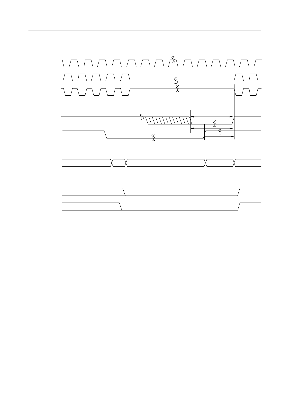
Standby Operation
CLK
XO
CLKA
RST*
STBY
t
RSTSTBY_S
t
W_RST
MSM7630¡ Semiconductor
t
RSTSTBY_H
t
STBYCLKA
CPU Operation
Operating
Suspend
Process
Suspend Resume Process Operating
RAS
CAS
Maintain the pin level on the STBY signal until the CPU has completed its suspend process and clock
signal CLKA has stopped.
After the STBY signal is released, the CPU will not resume until oscillation has stabilized (1024 t
CYC
* The RST signal is not necessary for self-refresh DRAM.
).
28/95

MSM7630¡ Semiconductor
Interrupt Process
CLK
XO
CLKA
EXTINT
The external interrupt signal EXTINT requests an interrupt to the CPU. The pin level on EXTINT
must be maintained until the CPU accepts the interrupt. Also, be sure to clear the interrupt source
within the interrupt routine.
29/95
 Loading...