E2U0057-38-21
¡ Semiconductor MSM7617
¡ Semiconductor
This version: Feb. 1999
Previous version: Aug. 1998
MSM7617
2-Channel Echo Canceler
GENERAL DESCRIPTION
The MSM7617 cancels echoes (acoustic or line echoes) generated in voice channels. It is a lowpower CMOS LSI device with two channels.
MSM7617 echo canceling is performed by digital signal processing. It negates echoes by
estimating the echo channel and then generating a pseudo-echo signal.
When used as an acoustic echo canceler, the MSM7617 can cancel acoustic echoes between
speaker and microphone that occur during hands-free speaking with car phones, conferencing
system phones, etc. When used as a line echo canceler, the MSM7617 can cancel line echoes
returned by hybrid impedance mismatches.
By setting its mode for use as a single cross-connected channel, the MSM7617 can cancel both
acoustic and line echoes.
Also, the MSM7617 can improve voice communication by using its howling detection, doubletalk detection, attenuation, and gain control functions to prevent and suppress howling levels,
and by using its center clipping function to suppress low level noise.
Furthermore, the MSM7617 can disable echo canceling during data communication with its 2100
Hz tone detector and 2100 Hz phase reversal detector. It also provides the ability to attenuate SIN
levels, to amplify SOUT levels, and to adjust input/output levels.
An economical and highly efficient echo canceler unit can be constructed by using a 2-channel
single-chip CODEC like the MSM7533 together with the MSM7617.
1/28

¡ Semiconductor MSM7617
FEATURES
•Echo canceler has two channels, which can be used for acoustic and line echoes. Set as a single
cross-connected channel, it can be used for both acoustic and line echoes.
•ITU-T G164/G165 standard tone disabler.
•PCM line level adjustment possible with SIN level attenuator (SA pin) and SOUT level
amplifier (SG pin). Can also be used for ERL amplification with the SIN level attenuator (SA
pin).
•RGC pin provides input/output adjustment mode (±6LR mode) that can prevent malfunction
due to excessive inputs without changing the RIN-ROUT input/output levels.
•Cancelable echo delay time: 55 ms (max.)
•Echo attenuation: 30 dB (typ.)
•Clock frequency: 18 to 20 MHz
19.2 MHz if using internal clock signal
•Power supply voltage: 4.5 to 5.5 V
•Package: 64-pin plastic QFP (QFP64-P-1414-0.80-BK)
•Product name: MSM7617-001GS-BK (m-law)
2/28

¡ Semiconductor MSM7617
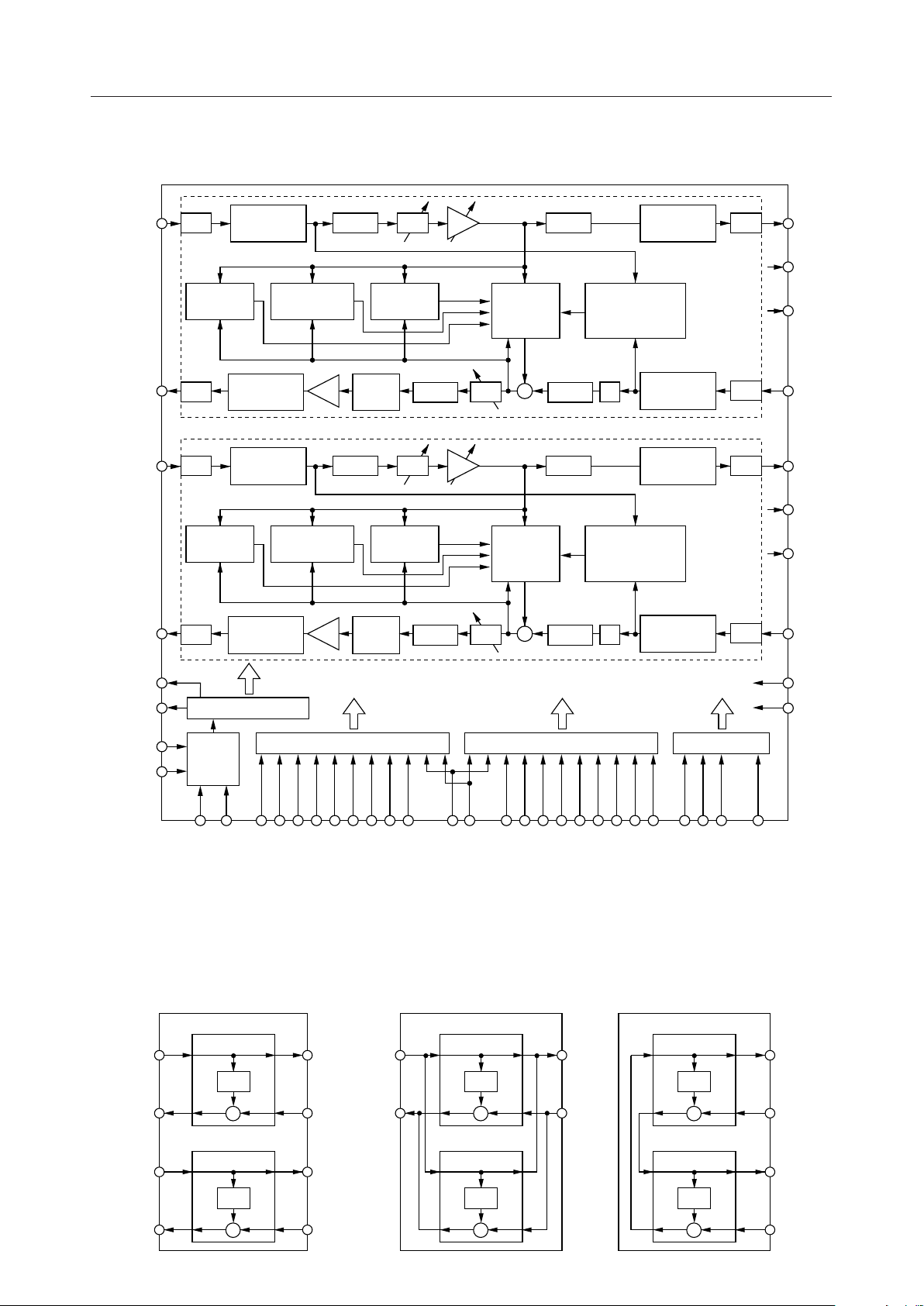
BLOCK DIAGRAM
RIN1
SOUT1
RIN2
SOUT2
Linear/
Non-linear
CH1
Howling
Detector
Non-linear/
Linear
Double Talk
Detector
ATT GC
Power
Calculator
Adaptive
FIR Filter
(AFF)
2100 Hz Tone,
Phase Reverse
Detector
S/P –6LR +6LR P/S
–
P/S
S/P –6LR +6LR P/S
Howling
Detector
Linear/
Non-linear
Non-linear/
Linear
Double Talk
Detector
SG
Center
Clip
Calculator
+6LR
ATT GC
Power
ATT
+
+
Adaptive
FIR Filter
–6LR
2100 Hz Tone,
Phase Reverse
(AFF)
SA
Detector
Non-linear/
Linear
Linear/
Non-linear
CH2
S/P
–
P/S
Linear/
Non-linear
SG
Center
Clip
+6LR
ATT
+
–6LR
+
SA
Non-linear/
Linear
S/P
ROUT1
DF1
WDT1
SIN1
ROUT2
DF2
WDT2
SIN2
SYNCO
SCKO Clock Generator
V
(PLL)
DD
V
(PLL)
SS
PLL
CLKIN
PWDWN
EC-A Controller EC-B Controller I/O Controller
HCL1
NLP1
RST1
ADP1
HD1
ATT1
SA10,11
SG10,11
RGC1011
ECM
ECDM0,1
NLP2
HCL2
RST2
ADP2
HD2
ATT2
SA20,21
SG20,21
GC20,21
SCK
SYNC2
SYNC1
IOM0,1
V
DD
V
SS
The above diagram shows internal connections for 2-channel parallel mode. The internal
connections for 2-channel serial I/O mode and 1-channel cross-connected mode are shown
below.
2-channel parallel I/O mode
CH1
RIN ROUT
AFF
SOUT SIN
+
ROUT1RIN1
SIN1SOUT1
RIN1
2-channel serial I/O mode
CH1
RIN ROUT
AFF
SOUT SIN
+
1-channel cross-connected mode
CH1
ROUT1
SIN1SOUT1
RIN ROUT
AFF
SOUT SIN
+
ROUT1
SIN1
CH2
RIN ROUT
AFF
SOUT SIN
+
CH2
ROUT2RIN2
SIN2SOUT2
RIN ROUT
AFF
SOUT SIN
+
CH2
RIN ROUT
AFF
SOUT SIN
+
ROUT2
SIN2
3/28

¡ Semiconductor MSM7617
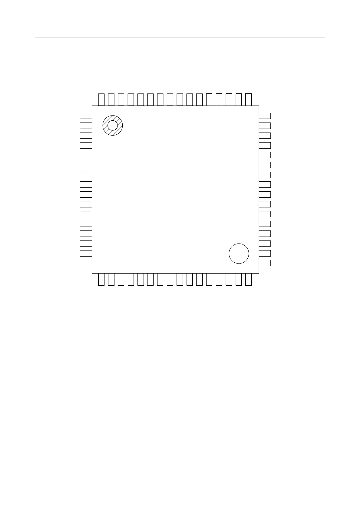
PIN CONFIGURATION (TOP VIEW)
SS
ROUT2
RIN2
SG21
SG20
SA21
55
SA20
54
53 VDD52 RGC21
51 RGC20
50 DF2
49 WDT2
HD2
64
ATT2
63
SOUT2
SIN2
62
61
V
60
59
58
57
56
RST2
ADP2
HCL2
SYNC2
V
DD
NLP2
IOM0
IOM1
SCK
ECM
NLP1
SS
10
11
12V
13SYNC1
14HCL1
15ADP1
16RST1
1
2
3
4
5
6
7
8
9
48
47
46
45
44
43
42
41
40
39
38
37 V
36 V
35 V
34 V
33 V
17
18
19
20
21
22
23
24
25
26
27
HD1
ATT1
SIN1
SOUT1
V
DD
RIN1
ROUT1
SG11
SG10
SA11
28VSS29RGC11
SA10
30RGC10
31DF1
32WDT1
(PLL)
V
SS
(PLL)
V
DD
CLKIN
V
SS
V
SS
TST
PWDWN
ECDM1
ECDM0
SCKO
SYNCO
DD
DD
DD
DD
DD
64-Pin Plastic QFP
4/28

¡ Semiconductor MSM7617
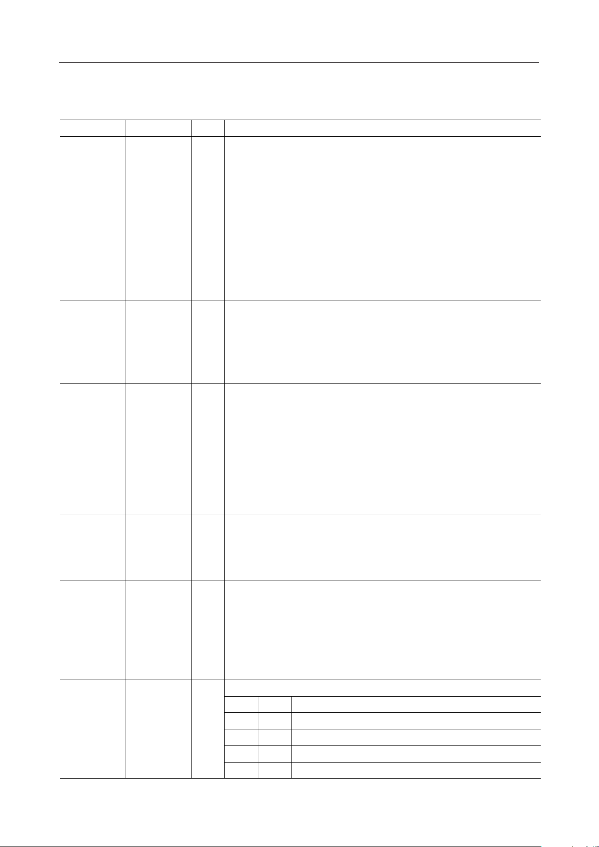
PIN DESCRIPTIONS
Pin Symbol Type Description
1 RST2 I Reset signal input pin for channel 2.
"L": Reset
"H": Normal operation
Input signals are invalid for 100 ms after reset (after RST returns to "H"
from "L") for setting initial values.
Input the basic clock during reset. Output pins will be placed in the
following states during reset.
Hi-Z: ROUT2, SOUT2
No effect: SYNCO, SCKO, ROUT1, SOUT1, DF1, WDT1
Previous state: DF2, WDT2
2 ADP2 I AFF coefficient control pin for channel 2.
This pin stops coefficient variation of the adaptive FIR filter (AFF), fixing the
coefficients. It allows once acquired AFF coefficients to be saved.
"H": Fixed coefficient mode
"L": Normal mode (variable coefficients)
3 HCL2 I Echo canceler disable pin for channel 2.
This pin disables the echo canceler and enables data from SIN to SOUT to be output
in "through mode". The input and output levels of SIN and SOUT are changed by the
setting of the SG and SA pins; therefore, to output data from SIN to SOUT in
"through mode", set the SA and SG pins to "0 dB".
It simultaneously clears the adaptive FIR filter coefficients.
"H": Disable mode
"L": Normal mode (echo canceller enabled)
4 SYNC2 I Sync signal input pin for channel 2 transmit/receive PCM data while in
parallel I/O mode.
Input the transmit/receive sync signal (8 kHz) of the PCM CODEC connected
to channel 2. Input "L" if not in parallel I/O mode.
6 NLP2 I NLP control pin for channel 2.
This pin controls center clipping, forcing SOUT2 output to the minimum
positive value when it is below –54 dBm0. It is effective for reducing
uncanceled echoes and low-level noise.
"H": Center clipping on
"L": Center clipping off
7
8
IOM0
IOM1
I Sets I/O mode of PCM data.
IOM1
IOM0
0
0
1
1
Mode Setting
0
2-channel parallel I/O mode
1
2-channel serial I/O mode
0
1-channel cross-connected mode
1
Inhibited
5/28

¡ Semiconductor MSM7617
PIN DESCRIPTIONS (Continued)
Pin Symbol Type Description
9 SCK I Common pin for channel 1 and channel 2. Clock input pin for PCM data
transmission.
Input the same clock as the transmit/receive clock of the PCM CODEC.
Frequencies below 128 kHz cannot be used in serial mode.
10 ECM I Not used. Fix input to "H".
11 NLP1 I NLP control pin for channel 1.
This pin controls center clipping, forcing SOUT1 output to the minimum
positive value when it is below –54 dBm0. It is effective for reducing
uncancelled echoes and low-level noise.
"H": Center clipping on
"L": Center clipping off
13 SYNC1 I Sync signal input pin for channel 1 transmit/receive PCM data while in 2-
channel parallel I/O mode, 2-channel serial I/O mode, or 1-channel cross-
connected mode.
Input the transmit/receive sync signal (8 kHz) of the PCM CODEC.
14 HCL1 I Echo canceler disable control pin for channel 1.
This pin disables the echo canceler and enables data from SIN to SOUT to be output
in "through mode". The input and output levels of SIN and SOUT are changed by the
setting of the SG and SA pins; therefore, to output data from SIN to SOUT in "through
mode", set the SA and SG pins to "0 dB".
It simultaneously clears the adaptive FIR filter coefficients.
"H": Disable mode
"L": Normal mode (echo canceler enabled)
15 ADP1 I AFF coefficient control pin for channel 1.
This pin stops coefficient variation of the adaptive FIR filter (AFF), fixing the
coefficients. It allows once acquired AFF coefficients to be saved.
"H": Fixed coefficient mode
"L": Normal mode (variable coefficients)
16 RST1 I Reset signal input pin for channel 1.
"L": Reset
"H": Normal operation
Input signals are invalid for 100 ms after reset (after RST returns to "H" from
"L") for setting initial values.
Input the base clock during reset. Output pins will be placed in the following
states during reset.
Hi-Z: ROUT1, SOUT1
No effect: SYNCO, SCKO, ROUT2, SOUT2, DF2, WDT2
Previous state: DF1, WDT1
6/28

¡ Semiconductor MSM7617
PIN DESCRIPTIONS (Continued)
Pin Symbol Type Description
17 HD1 I Howling detection control pin for channel 1.
This pin controls detection and canceling of howling generated by the
acoustics of handsfree telephones.
"L": Howling detector on
"H": Howling detector off
18 ATT1 I ATT control pin for channel 1.
This pin controls the ATT function for preventing howling with the
attenuators (ATT) provided on RIN and SOUT. When input is only on RIN,
the SOUT attenuator is activated. When there is no input on RIN or there is
input on both SIN and RIN, the RIN input attenuator is activated. Either the
ATT for the RIN output or the ATT for the SOUT is always activated in all
cases, and the attenuation of ATT is 6 dB.
"H": Attenuator off
"L": Attenuator on
Because the attenuator is inserted opposite the speaker, it is effective for
further reducing echo.
19 SOUT1 O PCM data output pin. Output signal changes depending on the setting of
the IOM pins (refer to the block diagram).
Data is always output on the rising edge of SCK. This pin is put in high
impedance state while there is no data or during reset.
In 2-channel parallel I/O mode, this pin becomes SOUT for channel 1 and
outputs the PCM signal synchronous with SYNC1. In 2-channel serial I/O
mode, this pin outputs the SOUT signal as a multiplexed PCM signal of
SOUT signal for channel 1 and channel 2 synchronous with SYNC1.
In 1-channel cross-connected mode, this pin becomes high impedance.
7/28

¡ Semiconductor MSM7617
PIN DESCRIPTIONS (Continued)
Pin Symbol Type Description
20 SIN1 I PCM data input pin. Pin use changes depending on the setting of the IOM
pins (refer to the block diagram).
In 2-channel parallel I/O mode, this pin becomes SIN for channel 1 and
inputs the PCM signal synchronous with SYNC1. In 2-channel serial I/O
mode, this pin sequentially inputs SIN as a multiplexed PCM signal from
channel 1 and channel 2 synchronous with SYNC1. In 1-channel cross-
connected mode, this pin becomes the cross-connected SIN pin for channel
1, and inputs the PCM signal synchronous with SYNC1.
Data is captured on the falling edge of SCK.
22 ROUT1 O PCM data output pin. Output signal changes depending on the setting of
the IOM pins (refer to the block diagram).
Data is always output on the rising edge of SCK. This pin becomes high
impedance while there is no data or during reset.
In 2-channel parallel I/O mode, this pin becomes ROUT for channel 1 and
outputs the PCM signal synchronous with SYNC1. In 2-channel serial I/O
mode, this pin outputs the ROUT signal as a multiplexed PCM signal of ROUT
signals for channel 1 and channel 2 synchronous with SYNC1.
In 1-channel cross-connected mode, this pin becomes the cross-connected
ROUT pin for channel 1, and outputs the PCM signal synchronous with SYNC1.
23 RIN1 I PCM data input pin. Pin use changes depending on the setting of the IOM
pins (refer to the block diagram).
In 2-channel parallel I/O mode, this pin becomes RIN for channel 1 and
inputs the PCM signal synchronous with SYNC1. In 2-channel serial I/O
mode, this pin sequentially inputs RIN as a multiplexed PCM signal from
channel 1 and channel 2 synchronous with SYNC1. In 1-channel cross-
connected mode, this pin is not used, and should be fixed at "L".
Data is captured on the falling edge of SCK.
8/28

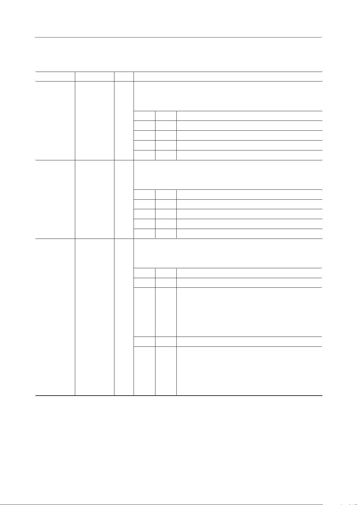
¡ Semiconductor MSM7617
PIN DESCRIPTIONS (Continued)
Pin Symbol Type Description
24
25
SG11
SG10
I S output gain control pins for channel 1 (refer to the block diagram).
These pins amplify the output level of SOUT. The gain level can be set even
during the echo canceler disable mode.
SG11
SG10
0
0
1
1
0
1
0
1
Gain Level
0 dB
+6 dB
+12 dB
Not used
26
27
29
30
SA11
SA10
RGC11
RGC10
I S input attenuator control pins for channel 1 (refer to the block diagram).
These pins attenuate the input level of SIN. Use them if ERL is large.
The attenuation level can be set even during the echo canceler disable mode.
SA11
I R input level control pins for channel 1 (refer to the block diagram).
Excessive input (PCM level is at maximum value) causes a malfanction.
Use these pins when there is a possibility of excessive input.
RGC11
SA10
0
0
1
1
RGC10
0
0
1
1
Attenuation Level
0
0 dB
1
–6 dB
0
–12 dB
1
Not used
Level Control Mode
0
Off
1
GC: On (control level = –20 dBm0)
By the R gain controller, levels from –20 to –11.5 dBm0 will
be suppressed to –20 dBm0 and those above –11.5 dBm0 will
always be attenuated by 8.5 dB. This is effective to prevent
excessive input and howling for hands-free applications.
0
Inhibited
1
±6LR: On
Applies –6 dB to excessive inputs using the level adjuster
provided on R and S I/O. Since +6 dB also is applied at the
output, the total level will not change, making this effective
against line echo.
9/28
 Loading...