E2U0036-28-81
¡ Semiconductor
This version: Aug. 1998
Previous version: Nov. 1996
MSM7583¡ Semiconductor
MSM7583
p/4 Shift QPSK MODEM
GENERAL DESCRIPTION
The MSM7583 is a CMOS IC for the p/4 shift QPSK modem developed for the digital cordless
telephone systems.
The device, which contains one system of modulator and two systems of demodulater, is
optimized for applications for cell stations in a cordless telephone system.
FEATURES
• Single +5 V Power Supply: 4.5 V to 5.5 V
(Modulator Block)
• Built in Root Nyquist Filter for Baseband Limitting (50% Roll-off)
• Ramp Bit for Burst Signal Rise-up (Fall-down) : 2 Symbols
• Built-in D/A converters for Analog Outputs of Quadrature Signal I/Q Components and
22
I + Q
• Differential I/Q Analog Output Type
• I/Q Output, DC Offset/Amplitude Adjustable
(Analog) Power Envelope Output.
(Demodulator Block)
• Built-in Diversity-corresponding Demodulation Circuit: 2 Systems
• Full Digital p/4 Shift QPSK Demodulation System
• Input IF Signal Frequency Selectable: 1.2/10.7/10.75/10.8 MHz
• Built-in Clock Recovery: 4 Circuits
• Transmit/Receive Independent Power-down Control capability
• Built-in Precise Analog Voltage Reference
• MCU Serial Interface for Mode Setting and Built-in Test Circuit
• Test Modes: Eye Pattern/AFC Compensating Signal/Phase Detection Signal Monitoring
Capability
• Transmission Speed: 384 kbps
• Low Power Consumption
Operating Mode: 16 mA Typ./Modulator (VDD = 5.0 V)
28 mA Typ./Demodulator (VDD = 5.0 V)
Whole Power-down Mode: 0.03 mA Typ. (VDD = 5.0 V)
• Package:
64-pin plastic QFP (QFP64-P-1414-0.80-BK)(Product name : MSM7583GS-BK)
1/23

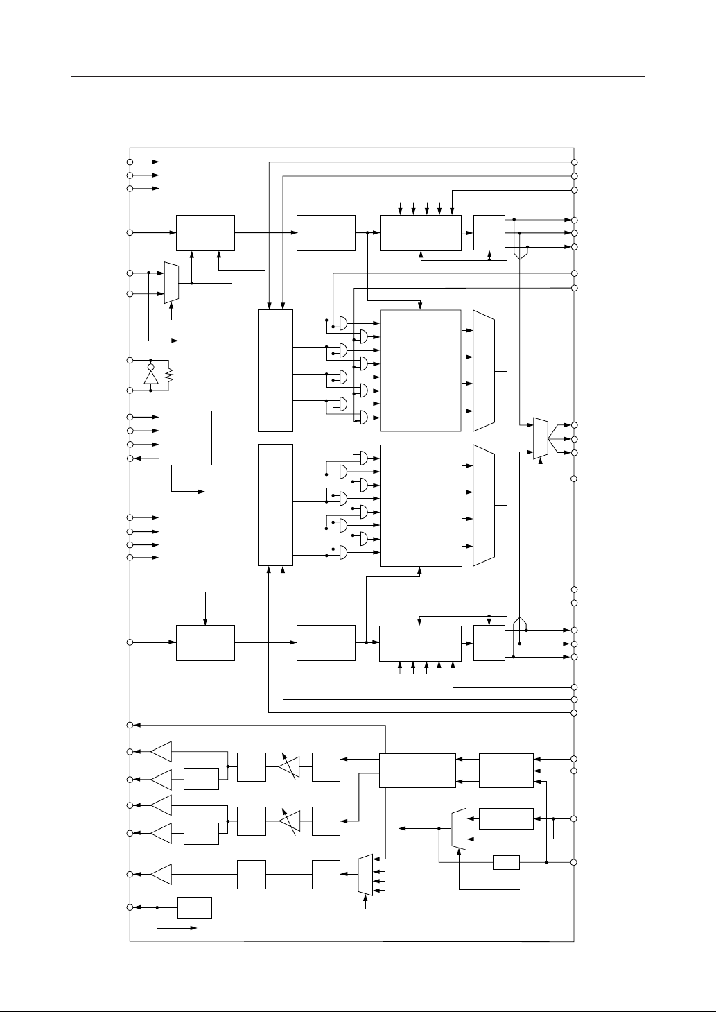
BLOCK DIAGRAM
MSM7583¡ Semiconductor
V
DGND
AGND
IFIN1
MCK
IFCK
DEN
EXCK
DIN
DOUT
PDN0
PDN1
PDN2
RESET
DD
SL41
SL41
SL41
SL41
Phase Detector Delay Detector
IFSEL0
S
(From CR)
AFC
Decision
E
L
IFSEL1
(From CR)
To each block
X2
X1
Control
Register
To each block
SL11
SL21
D
E
SL31
C
SL41
DPLL
S
E
L
S
E
L
SL11
D
SL21
E
C
SL31
SL41
DPLL
S
E
L
SLS11
SLS21
AFC1
RXD1
RXC1
RXSC1
RCW1
RPR1
RXD0
RXC0
RXSC0
RXSEL
IFN2
BST0
ENV
SG
RPR2
RCW2
RXCS2
Phase Detector Delay Detector
AFC
Decision
RXC2
RXD2
SL42
SL32
SL22
SL12
AFC2
SLS21
SLS22
I+
I–
Q+
Q–
+1
DC Offset
–1
Adjust
LPF
I output gain adjust
D/A
Root Nyquist
LPF
S/P
MAPPING
TXD
TXW
+1
DC Offset
–1
Adjust
+1
LPF
Q output gain adjust
LPF
VREF
To internal SG
D/A
D/A
3.84 MHz
To D/A
To monitor
output of
each block
TEST1, TEST0 (From CR)
S
E
L
PLL
1/10
TXCEL (From CR)
384 kHZ
TXCI
TXCO
2/23

PIN CONFIGURATION (TOP VIEW)
NC
X2
X1
RPR2
AFC2
64
63
62
61
60
1
NC
2
IFCK
3
MCK
4
DGND
5
IFIN2
6
DGND
7
IFIN1
8
DGND
9
V
DD
10
DOUT
11
DIN
12
EXCK
13
DEN
14
RESET
15
PDN0
16 33
PDN1
RCW2
59
RPR1
58
AFC1
57
RCW1
56
RXSC0
55
RXC0
54
RXD0
53
RXSEL
52
RXSC2
51
RXC2
50
RXD2
49
48
47
46
45
44
43
42
41
40
39
38
37
36
35
34
MSM7583¡ Semiconductor
NC
SLS22
SLS12
RXSC1
RXC1
RXD1
SLS21
SLS11
V
DD
ENV
Q–
Q+
I–
I+
SG
AGND
NC : No connect pin
17
NC
18
PDN2
19
BSTO
20
TXW
21
22
23
24
TXD
TXCO
64-Pin Plastic QFP
TXCI
NC
25
NC
26
NC
27
NC
28
NC
29
NC
30
NC
31
NC
32
NC
3/23

MSM7583¡ Semiconductor
PIN AND FUNCTIONAL DESCRIPTIONS
TXD
Transmit data input for 384 kbps.
TXCI
Transmit clock input.
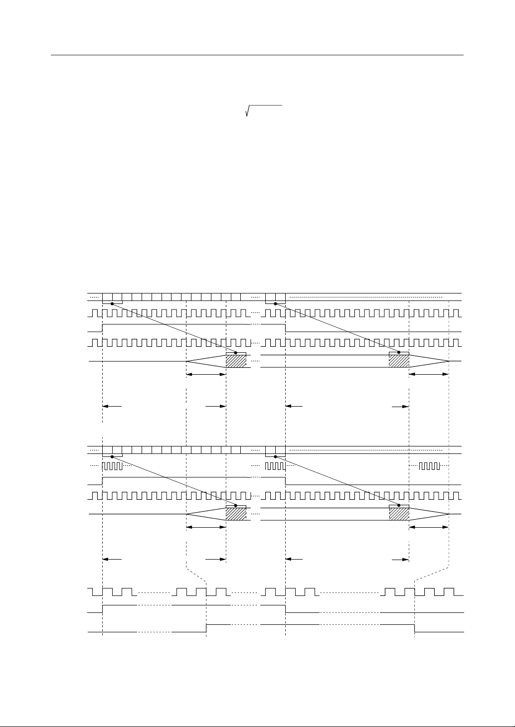
When the control register CR0 - B6 is “0”, a 384 kHz clock pulse synchronous with TXD should
be input to this pin. This clock pulse should be continuous because this device uses APLL to
generate internal clock pulses.
When CR0 - B6 is “1”, a 3.84 MHz clock pulse should be input to this pin. When the 3.84 MHz
clock pulse is applied to TXCI, TXCO outputs a 384 kHz clock pulse, which is generated by
dividing the TXCI input by 10. The transmit data, synchronous 384 kHz clock pulse, should be
input to the TXD. In this case the device does not use APLL, and the 3.84 MHz clock pulse need
not be continuous. (Refer to Fig. 1.)
TXCO
Transmit clock output.
When CR0 - B6 is “0”, TXCO outputs the 384 kHz clock pulse (APLL output) for monitoring
purposes. When CR0 - B6 is “1”, this pin outputs a 384 kHz clock pulse generated by dividing
the TXCI input by 10. (Refer to Fig. 1.)
TXW
Transmit data window signal input.
The transmit timing signal for the burst data is input to the device through this pin. If TXW pin
is “1”, modulation data is output. (Refer to Fig. 1.)
I+, I–
Quadrature modulation signal I component differential analog outputs.
The level of the outputs is 500 mVpp with 1.6 Vdc as center value. The output pin load
conditions are: R ≥ 10 kW, C £ 20 pF. The gain of these pins can be adjusted using the control
registers CR1 - B7 to B4, and the offset voltage at the I– pin can be adjusted using CR3 - B7 to
B3.
Q+, Q–
Quadrature modulation signal Q component differential analog outputs.
The level of the outputs is 500 mVpp with 1.6 Vdc as center value. The output pin load
conditions are: R ≥ 10 kW , C £ 20 pF. The gain of these pins can be adjusted using the control
registers CR1 - B3 to B0, and the offset voltage at the Q– pin can be adjusted using CR4 - B7 to
B3.
4/23

ENV
MSM7583¡ Semiconductor
Quadrature modulation signal envelope (
22
I + Q
) output.
Its output level is 500 mVpp with 1.6 Vdc as a center value. The output pin load conditions are:
R ≥ 10 kW , C £ 20 pF. The gain of this output can be adjusted using the control registers CR2
- B7 to B4.
This pin is also used to monitor eye pattern, AFC compensating signal, and phase detection of
the demodulator block during the test mode. Refer to the description of the control register for
details.
BSTO
Modulation burst window signal output.
The burst position for the I/Q baseband modulation output is output. (Refer to Fig. 1.)
(1) CR0 - B6 ="0".
TXD
TXCI
(384 kHz)
TXW
TXCO
(384 kHz)
I, Q
D0 D1
D2 D3 D4 D5D6D7 D8D9
Delay of 6.25 symbols
Ramp rise-up
2 symbols
D13D12D11D10
Dn-1 D
n
Ramp fall-down
2 symbols
Delay of 6.25 symbols
(2) CR0 - B6 ="1".
TXD
D0 D1
TXCI
(3.84 MHz)
TXW
TXCO
(384 kHz)
I, Q
TXCI
(384 kHz)
12 8910 N
TXW
BSTO
D2 D3 D4 D5D6D7 D8D9
Ramp rise-up
2 symbols
Delay of 6.25 symbols
Figure 1 Transmitter Timing Diagram
D13D12D11D10
Dn-1 D
n
Ramp fall-down
2 symbols
Delay of 6.25 symbols
N+1 N+2 N+16 N+17 N+18 N+19
5/23

MSM7583¡ Semiconductor
SG
Internal reference voltage output.
The output voltage is about 2.0 V. A bypass capacitor should be connected between this pin
and the AGND pin. The external SG voltage, if necessary should be used via buffer.
RESET
Control register reset.
When this pin is set to "0", the register is reset to the initial value.
The reset signal input width is 200 ns or more.
PDN0, PDN1, PDN2
Inputs for power-down control.
PDN0 controls the standby/communication modes, PDN1 controls the modulator, and PDN2
controls the demodulator. Refer to Table 1 for details.
Table 1 Power Down Control
PDN1
0
0—1
100
111
Standby Mode
Communication
Mode
V
DD
PDN0
+5 V power supply voltage.
AGND
Analog signal ground.
PDN2
—0
Function
All power-down.
Modulator power is off (VREF and PLL power is also off).
Demodulator power is on.
Modulator power is off (VREF and PLL power is on).
I and Q outputs are in a high-impedance state.
Only demodulator clock recovery block power is on.
Modulator power is on.
Only demodulator clock recovery block power is on.
Modulator power is off (VREF and PLL power is on).
I and Q outputs are in a high-impedance state.
Demodulator power is on.
Modulator power is on.
Demodulator power is on.
Mode
Mode A
Mode B
Mode C
Mode D110
Mode E101
Mode F
DGND
Digital signal ground.
AGND and DGND are not connected in the device. This pin should be tied to the AGND pin
on the PCB as close as possible from the device.
AGND and DGND should be connected as close as prossible on the PC board.
6/23

MSM7583¡ Semiconductor
MCK
Master clock input.
The clock frequency is 19.2 MHz.
IFIN1, IFIN2
Modulated signal inputs for the demodulator block.
Select the IF frequency from 1.2 MHz, 10.7 MHz, 10.75 MHz, and 10.8 MHz based on CR0 - B4
and B3. IFIN1 is for Channel 1, and IFIN2 for Channel 2.
IFCK
Clock signal input for demodulator block IF frequency (10.7 MHz or 10.75 MHz).
If the IF frequency is 10.7 MHz, 19.0222 MHz should be supplied. When it is 10.75 MHz, 19.1111
MHz should be supplied. When the IF frequency is 1.2 MHz or 10.8 MHz, set this pin to “0”
or “1”. (Refer to Fig. 2.)
X1, X2
Crystal oscillator connection pins.
When supplying a 19.0222 MHz or 19.1111 MHz clock to IFCK, use these pins. (Refer to Fig. 2.)
When IFIN = 10.7 MHz or 10.75 MHz
MSM7583
IFCKX2X1
19.0222 MHz or 19.1111 MHz
Figure 2 How to Use IFCK, X1, and X2
When IFIN = 1.2 MHz or 10.8 MHz
MSM7583
IFCKX2X1
7/23
 Loading...