OKI MSM7582TS-K, MSM7582BTS-K Datasheet

E2U0035-16-X2
¡ Semiconductor MSM7582/7582B
¡ Semiconductor
This version: Jan. 1998
Previous version: Nov. 1996
MSM7582/7582B
p/4 Shift QPSK MODEM
GENERAL DESCRIPTION
The MSM7582/7582B are CMOS ICs for the p/4 shift QPSK modem developed for the digital
cordless telephone systems.
The devices are designed for Personal and Cell station applications, the MSM7582B is the
improved MSM7582 in modulator burst rise-up and fall-down characteristics.
FEATURES
••
• Single Power Supply (VDD: 2.7 V to ␣ 3.6 V)
••
(Modulator Block)
••
• Built-in Root Nyquist Filter for Baseband Limiting (50% Roll-off)
••
••
• Ramp Bit for Burst Signal Rise-up:
••
MSM7582/1.75 symbols
MSM7582B/2.0 symbols
••
• Ramp Bit for Burst Signal Fall-down:
••
MSM7582/2.75 symbols
MSM7582B/2.0 symbols
••
• Built-in D/A converters for Analog Output of Quadrature Signal I/Q Components and Power
••
Envelope Output
••
• Differential I/Q Analog output format
••
••
• I/Q Output DC Offset / Gain Adjustable
••
I2 + Q
2
(Demodulator Block)
••
• Full Digital System, p/4 shift QPSK Demodulation
••
••
• Input IF signal Frequency Selectable: 1.2/10.7/10.75/10.8 MHz
••
••
• Built-in Clock Recovery: 4 Circuits useful for Cell station
••
(Common)
••
• Various Power-down Modes: Tramsmit/Receive Independant
••
••
• Built-in Precise Analog Voltage Reference
••
••
• MCU Serial Interface for Mode setting and Built-in Test circuit
••
••
• Test Modes: Eye pattern / AFC Compensating Signal / Phase Detection Signal, possible to
••
monitor
••
• Transmission Speed: 384 kbps
••
••
• Low Power consumption
••
Operating mode : 15 mA Typ. / Modulator (VDD = 3.0 V)
: 9 mA Typ. / Demodulator (VDD = 3.0 V)
Whole system Power-down mode: 0.01 mA Typ. (VDD = 3.0 V)
••
• Package:
••
32-pin plastic TSOP (TSOPI32-P-814-0.50-1K)(Product name : MSM7582TS-K)
(Product name : MSM7582BTS-K)
1/24

¡ Semiconductor MSM7582/7582B
2/24
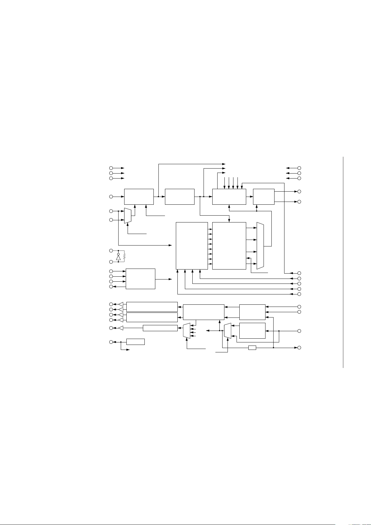
BLOCK DIAGRAM
IFIN
AGND
DGND
V
DD
Phase Detector Delay Detector
IFCK
MCK
X1
DEN
EXCK
DIN
DOUT
S
E
L
X2
Control
Register (CR)
To each
block
PDN0
PDN1
PDN2
AFC
DPLL
Decision
Unit
RXC
RXD
S
E
L
SLS1
SLS2
+
1
-
1
+
1
-
1
+
1
I+
I–
Q+
Q–
ENV
Root Nyquist
LPF
S
E
L
S/P
MAPPING
S
E
L
APLL
TXD
TXW
TXCI
1/10
TXCO
SG
To internal SG
To each block
IFSEL0
(From CR)
IFSEL1
(From CR)
SL4
SL3
SL2
SL1
To monitor output
of each block
To modem ENV
PS/CS
RPR
RCW
AFC
TEST1, TEST0
(From CR)
To
Monitor
output of
each block
TXCSEL
(From CR)
3.84 MHz
384 kHz
Decoder
ENV D/A CONV
VREF
I ± D/A CONV
Q ± D/A CONV
To D/A

¡ Semiconductor MSM7582/7582B
PIN CONFIGURATION (TOP VIEW)
AGND
SG
I+
I–
Q+
Q–
ENV
PDN0
PDN1
PDN2
V
DD
SLS1
SLS2
RCW
AFC
RPR
10
11
12
13
14
15
16
1
2
3
4
5
6
7
8
9
32-Pin Plastic TSOP
32
31
30
29
28
27
26
25
24
23
22
21
20
19
18
17
DGND
IFIN
TXCI
TXCO
TXD
TXW
DEN
EXCK
DIN
DOUT
MCK
RXD
RXC
IFCK
X2
X1
3/24

¡ Semiconductor MSM7582/7582B
PIN AND FUNCTIONAL DESCRIPTIONS
TXD
Transmit data input for 384 kbps.
TXCI
Transmit clock input.
When the control register CR0 – B6 is “0”, a 384 kHz clock pulse synchronous with TXD should
be input to this pin. This clock pulse should be continuous because these devices use APLL to
generate the internal clock pulse.
When CR0 – B6 is “1”, a 3.84 MHz clock pulse should be input to this pin. When the 3.84 MHz
clock pulse is applied, TXCO outputs a 384 kHz clock pulse, which is generated by dividing the
3.84 MHz to TXCI by 10. The transmit data, synchronous 384 kHz clock pulse, should be input
to the TXD. In this case the devices do not use APLL, and the 3.84 MHz clock pulse need not be
continuous. (Refer to Fig. 1.)
TXCO
Transmit clock output.
When CR0 - B6 is “0”, TXCO outputs the 384 kHz clock pulse (APLL output) for monitoring
purposes. When CR0 – B6 is “1”, this pin outputs a 384 kHz clock pulse generated by dividing
the TXCI input by 10. (Refer to Fig. 1.)
When CR0 – B6 = “0” and CR5 – B7 = “1”, this pin outputs the burst timing position.
TXW
Transmit data window input.
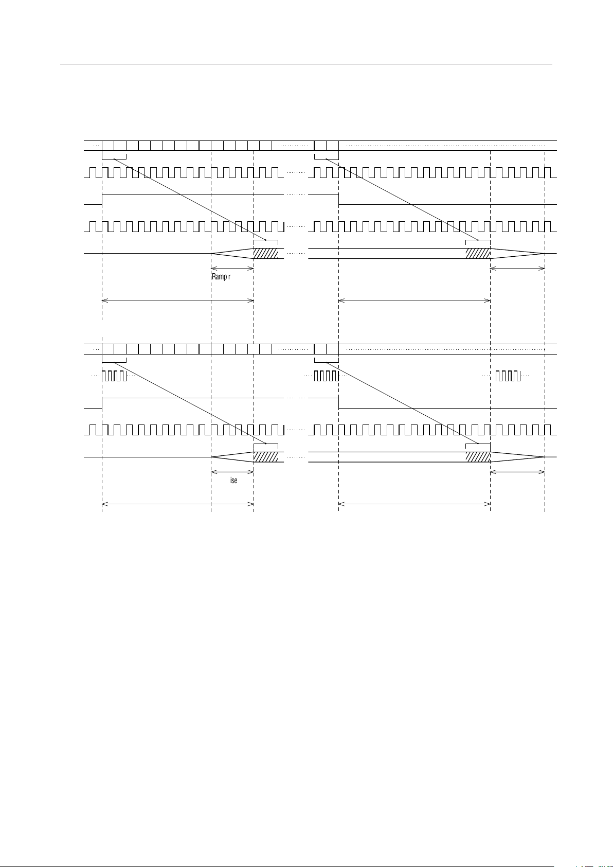
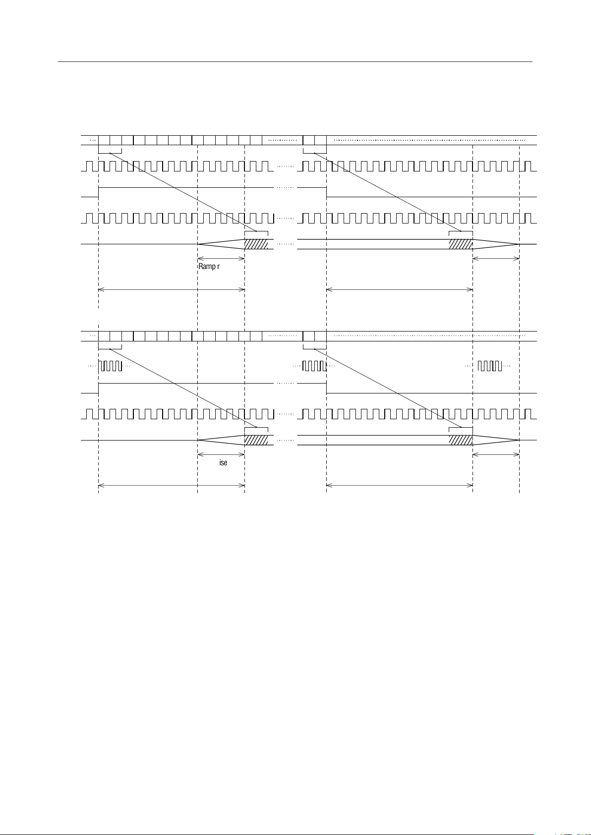
The transmit timing signal for the burst data is input to the device pin. If TXW is “1”, the
modulation data is output. However, the MSM7582 is different from the MSM7582B in the ramp
response time for burst rise-up and burst fall-down of I, Q modulated outputs, as shown in the
table below. (Refer to Fig, 1-1 for the MSM7582 and Fig, 1-2 for the MSM7582B)
MSM7582 MSM7582B
Ramp Rise-up 1.75 symbols 2 symbols
Ramp Fall-down 2.75 symbols 2 symbols
The TXCO burst position output timing discribed before, is different, according to this table.
4/24

¡ Semiconductor MSM7582/7582B
,
MSM7582
(1) CR0 – B6 = "0"
D0 D1 D2 D3 D4 D5 D6 D7 D8 D9
TXD
TXCI
(384 kHz)
TXW
TXCO
(384 kHz)
I, Q
Delay of 6.25 symbols
(2) CR0 – B6 = "1"
D0 D1 D2 D3 D4 D5 D6 D7 D8 D9
TXD
TXCI
(3.84 MHz)
TXW
TXCO
(384 kHz)
I, Q
D10 D11 D12 D13
Ramp rise-up
1.75 symbols
D10 D11 D12 D13
Dn-1
Dn-1
Dn
Ramp
Delay of 6.25 symbols
Dn
Fall-down
2.75 symbols
Delay of 6.25 symbols
Ramp rise-up
1.75 symbols
Delay of 6.25 symbols
Figure 1-1 Transmit Timing Diagram
Ramp
Fall-down
2.75 symbols
5/24

¡ Semiconductor MSM7582/7582B
,
MSM7582B
(1) CR0 – B6 = "0"
D0 D1 D2 D3 D4 D5 D6 D7 D8 D9
TXD
TXCI
(384 kHz)
TXW
TXCO
(384 kHz)
I, Q
Delay of 6.25 symbols
(2) CR0 – B6 = "1"
D0 D1 D2 D3 D4 D5 D6 D7 D8 D9
TXD
TXCI
(3.84 MHz)
TXW
TXCO
(384 kHz)
I, Q
D10 D11 D12 D13
Ramp rise-up
2 symbols
D10 D11 D12 D13
Dn-1
Dn-1
Dn
Ramp fall-down
Delay of 6.25 symbols
Dn
2 symbols
Delay of 6.25 symbols
Ramp rise-up
2 symbols
Delay of 6.25 symbols
Ramp fall-down
2 symbols
Figure 1-2 Transmit Timing Diagram
I+, I–
Quadrature modulation signal I component differential analog outputs.
Their output levels are 500 mVpp with 1.6 Vdc as the center value. The output pin load conditions
are: R ≥ 10 kW, C ≤ 20 pF. The gain of these pins can be adjusted using the control register CR1
– B7 to B4, and the offset voltage at the I– pin can be adjusted using CR3 – B7 to B3.
Q+, Q–
Quadrature modulation signal Q component differential analog outputs.
Their output levels are 500 mVPP with 1.6 Vdc as the center value. The output pin load conditions
are: R ≥ 10 kW, C ≤ 20 pF. The gain of these pins can be adjusted using the control register CR1
– B3 to B0, and the offset voltage at the Q– pin can be adjusted by using CR4 – B7 to B3.
6/24

¡ Semiconductor MSM7582/7582B
ENV
Quadrature modulation signal envelope (
I2 + Q
2
)output.
Its output level is 500 mVPP with 1.6 Vdc as a center value. The output pin load conditions are
: R ≥ 10 kW, C ≤ 20 pF. The gain of this output can be adjusted using the control register CR2 – B7
to B4.
This pin is also used to monitor eye pattern, AFC Compensating signal, and phase defection of
the demodulator block during the test mode. Refer to the description of the control register for
details.
SG
Internal reference voltage output.
The output voltage is about 2.0 V. A bypass capacitor should be connected between this pin and
the AGND pin.
PDN0, PDN1, PDN2
Inputs for power-down control.
PDN0 controls the standby / communication modes, PDN1 controls the modulator, and PDN2
controls the demodulator. Refer to Table 1 for details.
Table-1 Power Down Control
PDN0
Standby
Mode
Communication
Mode
PDN2 PDN1
0 0/1 1
000
010
100
101
110
111
Function
All power-down. The control register is reset.
All power-down. The control register is not reset.
Modulator power is off (VREF and PLL power are also off).
Demodulator power is on.
Modulator power is off (VREF and PLL power is on).
I and Q outputs are in a high-impedance state.
Only demodulator clock recovery block power is on.
Modulator power is on
Only demodulator clock recovery block power is on.
Modulator power is off (VREF and PLL power is on).
I and Q outputs are in a high-impedance state.
Demodulator power is on.
Modulator power is on
Demodulator power is on.
Mode
Mode A
Mode B
Mode C
Mode D
Mode E
Mode F
Mode G
V
DD
+3 V power supply voltage.
AGND
Analog signal ground.
DGND
Digital signal ground.
AGND and DGND are not connected in the device. This pin should be tied to the AGND pin on
the PCB as close as possible from the device.
7/24

¡ Semiconductor MSM7582/7582B
MCK
Master clock input.
The clock frequency is 19.2 MHz.
IFIN
Modulated signal input for the demodulator block.
Select the IF frequency from 1.2 MHz, 10.7 MHz, 10.75 MHz, and 10.8 MHz, based on CR0 – B4
and B3.
IFCK
Clock signal input for demodulator block IF frequencies (10.7 MHz or 10.75 MHz).
If the IF frequency is 10.7 MHz, 19.0222 MHz should be supplied. When it is 10.75 MHz, 19.1111
MHz should be supplied. When the IF frequency is 1.2 MHz or 10.8 MHz, set this pin to “0” or
“1”. (Refer to Fig. 2.)
X1, X2
Crystal oscillator connection pins.
When supplying a 19.0222 MHz or 19.1111 MHz clock to IFCK, use these pins (Refer to Fig. 2.)
When IFIN = 10.7 MHz or 10.75 MHz
MSM7582/7582B
X1 IFCK
19.0222 MHz or 19.1111 MHz
X2
When IFIN = 1.2 MHz or 10.8 MHz
MSM7582/7582B
X1 IFCK
X2
Figure 2 How to Use IFCK, X1, and X2
RXD, RXC
Receive data and clock output. When power is turned on, the outputs of circuits selected by SLS1
and SLS2 appear at these pins. (Refer to Fig. 3)
RXD1
RXC
SLS2
SLS1
The recovery data and clock pulse are selected
asynchronously using the SLS signals.
Figure 3 RXD and RXC Timing Diagram
8/24
 Loading...