E2U0025-29-82
¡ Semiconductor
¡ Semiconductor
This version: Aug. 1999
Previous version: Jan. 1998
MSM7575
MSM7575
Multi-Function PCM CODEC
GENERAL DESCRIPTION
The MSM7575, developed for advanced digital cordless telephone systems, is a single channel
full duplex CODEC which performs mutual transcoding between the analog voice band signal
and the 64 kbps PCM serial data.
This device performs DTMF tone and several kinds of tone generation, transmit/receive data
mute and gain control, side-tone pass and its gain control, and VOX function.
Using advanced circuit technology, this device operates from a single 3 V power supply and
provides low power consumption.
FEATURES
••
• Single 3 V Power Supply Operation VDD: 2.7 V to ␣ 3.6 V
••
••
• Transmit/Receive Full-Duplex Single Channel Operation
••
••
• Transmit/Receive Synchronous Mode Only
••
••
• PCM Interface Data Format :
••
••
• Serial PCM Transmission Data Rate : 64 kbps to 2048 kbps
••
••
• Low Power Consumption
••
Operating Mode : 24 mW Typ. (V
Power-Down Mode : 0.03 mW Typ. (V
••
• Two Analog Input Amplifier Stages: Externally Gain Adjustable
••
••
• Analog Output Stage
••
••
• Master Clock Frequency : 9.600/19.200 MHz Selectable
••
••
• Transmit/Receive Mute, Transmit/Receive Programmable Gain Control
••
••
• Side Tone Path with Programmable Attenuation (8-step Level Adjustment)
••
••
• Built-in DTMF Tone Generator
••
••
• Built-in Various Ringing Tones Generator
••
••
• Built-in Various Ring Back Tone Generator
••
••
• Control by Serial MCU Interface
••
••
• Built-in VOX Control
••
Transmit side : Voice/Silence Signal Detect
Receive side : Background Noise Generation
••
• Built-in Op-amps and Analog Switches for Various Analog Interfaces.
••
••
• Package:
••
64-pin plastic QFP (QFP64-P-1414-0.80-BK)(Product name : 7575GS-BK)
A-law/µ-law/linear (2's complement) Selectable
= 3.0 V)
DD
= 3.0 V)
DD
Push-pull Drive (direct drive of 350 W␣ + 120 nF)
1/25

2/25
¡ Semiconductor
MSM7575
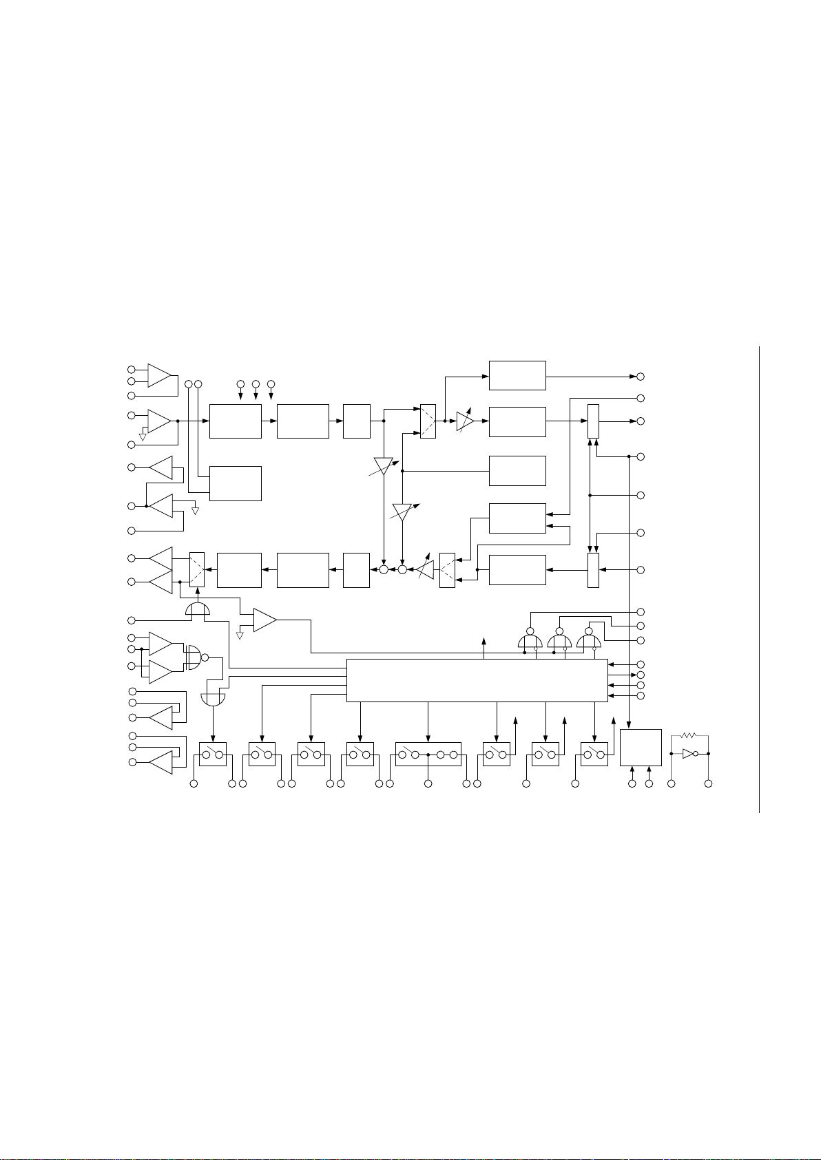
BLOCK DIAGRAM
AIN2
GSX2
VOXI
PCMSO
Prefilter
+
-
AIN1+
GSX1
AOUT-
BPF
P
/
S
XSYNC
RSYNC
PCMRI
S
/
P
Postfilter
LPF
BCLK
PWI
AOUT+
-1
VFRO
AIN1-
-1
VOXO
Compand
Voice Signal
Detect
A/D
D/A
++
EXCK
PDN/
RESET
MCU Interface
Clock/
Timing
ATT
ATT
ATT
+
-
-
+
SAO
-1
ATT
Expand
VREF
+
RINGC
AVIN
REF1
+
-
+
REF2
+
AIN3-
GSX3
AIN3+
+
AIN4-
GSX4
AIN4+
IO1
IO2
SW1
IO3
IO4
SW2
IO5
IO6
SW3
IO7
IO8
SW4
IO9
IO10
SW5
IO11
SW6
IO12
SW7
IO13
SW8
IO14
SW9
V
DD
V
DD
V
DD
MCK
X1
X2
DEN
DOUT
DIN
TOUT1
TOUT2
TOUT3
SGB
SG
AG
DG
V
DD
Tone GEN.
Back ground
Noise Gen.
To each circuit

¡ Semiconductor
PIN CONFIGURATION (TOP VIEW)
MSM7575
VOXO
DOUT
DIN
EXCK
DEN
PCMRI
PCMSO
RSYNC
XSYNC
BCLK
DG
IO1
10
11
12
13
MCKX2NC
64
63
1
2
3
4
5
6
7
8
9
62
NC
61
X1
PDN/RESETNCTOUT3
60
59
58
57
TOUT2
TOUT1
56
55
RINGC
VDD
54
53
REF2
52
REF1
51
AVIN
50
NC
49
48VOXI
47
46
45
44
43
42
41
40
39
38
37
36
AOUT+
AOUT-
PWI
VFRO
SAO
GSX2
AIN2
GSX1
AIN1-
AIN1+
GSX4
AIN4-
AIN4+
14
IO2
15
IO3
16
IO4 AIN3+
NC : No connect pin
17
IO5
18
IO6
19
IO7
20
IO8
21
22
23
24
IO9
IO10
IO11
IO12
64-Pin Plastic QFP
25
IO13
26
IO14
27
NC
28
NC
29
NC
30
SGB
31
SG
32
AG
35
34
33
GSX3
AIN3-
3/25

¡ Semiconductor
MSM7575
PIN AND FUNCTIONAL DESCRIPTIONS
AIN1+, AIN1–, AIN2, GSX1, GSX2
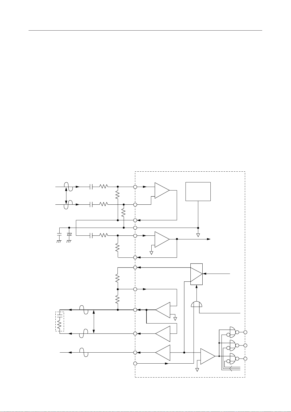
Transmit analog input and the output for transmit gain adjustment. The pin AIN1– (AIN2)
connects to the inverting input of the internal transmit amplifier, and the pin AIN1+ connects to
the non-inverting input of the internal transmit amplifier. The pin GSX1 (GSX2) connects to
output of the internal transmit amplifier. Gain adjustment should be referred to Fig. 1.
VFRO, AOUT+, AOUT–, PWI, SAO, RINGC
Used for the receive analog output and the output for receive gain adjustment. VFRO is an
output of the receive filter. AOUT+ and AOUT– are differential analog signal outputs which can
directly drive ZL = 350 W + 120 nF or the 1.2 kW load. Gain adjustment should be referred to Fig.
1.
The ORed signal with the control register data CR4-B5 and the external pin RINGC determines
the output pins (AOUT+ and AOUT- /SAO+ and SAO-) for the speech signal and an acoustic
component of the sounder tone, DTMF tone, R tone, F tone, various kinds of tones at either the
VFRO pin or the SAO pin.
Differential
Analog Input
0.1 mF
Vi
10 mF
+
–
Transmit Gain: V
= (R2/R1) ¥ (R4/R3)
Receive Gain: Vo/V
= 2 ¥ (R6/R5)
= 120 nF
Z
L
+ 350 W
C1
C1 R1
C2
V
R1
R3
GSX2
VFRO
O
R2
R4
/Vi
R5
R6
Differential
Analog
Output
R2
AIN1–
AIN1+
GSX1
SG
AIN2
GSX2
VFRO
PWI
AOUT–
AOUT+
–
+
–
+
–
+
–1
V
REF
to ENCODER
SELECT
from
DECODER
from MCU INT.
TOUT1
Sounder Output
Signal
SAO
RINGC
+1
Figure 1 Analog Input/Output Interface
+
–
TOUT2
TOUT3
from MCU INT.
4/25

¡ Semiconductor
MSM7575
TOUT1, TOUT2, TOUT3
These are pins for outputs of the NOR gates whose inputs are the comparator output signal
between the SAO output level and the SG level, and each register signal stored by the MCU
interface.
The each output is NOR-gated with the comparator output and the invented signal of CR1-B7 at
TOUT3, the inverted signal of CR1-B6 at TOUT2, and the inverted signal of CR1-B5 at TOUT1.
AVIN, REF1, REF2
These pins are for inputs of two comparators internal to the device. AVIN is connected to each
non-inverting input of comparator1 and comparator2. REF1 is connected to an inverting input
of comparator1 and REF2 is connected to an inverting input of comparator2. The output of each
comparator is connected to the input of ENOR. The interval analog switch SW1 is ON/OFF
controlled by the output which is the logical OR of the ENOR and the CR5-B7 signal. When CR5B7 is at "0", the SW1 is turned to OFF if AVIN is within the voltage range of REF1 and REF2 and
the SW1 is turned to ON if AVIN is out of the voltage range of REF1 and REF2.
AIN3+, AIN3-, GSX3, AIN4+, AIN4-, GSX4
These pins are for inputs and outputs of the internal op-amps. Refer to BLOCK DIAGRAM for
the connection.
IO1 to IO14
These pins are for inputs and outputs of the internal analog switch. Refer to BLOCK DIAGRAM
and FUNCTIONAL DESCRIPTION for the connection and the control method.
X1, X2
Crystal oscillator connection pins. X2 is for the clock output pin. When a conventional external
clock is used, X1 should be connected to the ground, X2 should be left open, and the clock should
be input to the MCK pin.
For the use of a self-oscilation circut
MSM7575
X1
X2
MCK
For the use of an external clock
MSM7575
X1
X2
MCK
9.6 MHz or
19.2 MHz
9.6 MHz or
19.2 MHz
Figure 2 Connection to a Crystal Oscillator or an External Clock
5/25

¡ Semiconductor
MSM7575
SG, SGB
Analog signal ground output.
The output voltage is about 1.4 V. The bypass capacitors (10 µF in parallel with 0.1 µF ceramic
type) should be put between this pin and AG to get the specified noise characteristics. This
output voltage is 0 V during power-down.
AG
Analog ground.
DG
Digital ground.
This ground is separated from the analog signal ground(AG) in this device. The DG pin must be
kept as close to the AG pin possible on the PCB.
V
DD
+3 V power supply.
PDN/RESET
Power down and reset control input.
“L” level makes the whole chip enter to power down state, and, at the same time, all of control
register data are reset to the initial state. Set this pin to “H” level during normal operating mode.
The power down state is controlled by a logical OR with CR0-B5 of the control register. When
using the pin PDN/RESET for the power down and reset control, CR0-B5 should be set to digital
“0”.
MCK
Master clock input.
The frequency must be 9.6 MHz or 19.2 MHz. The applied clock frequency is selected by the
control register data CR0-B6. The master clock signal is allowed to be asynchronous with BCLK,
XSYNC, and RSYNC.
PCMSO
Transmit PCM data output.
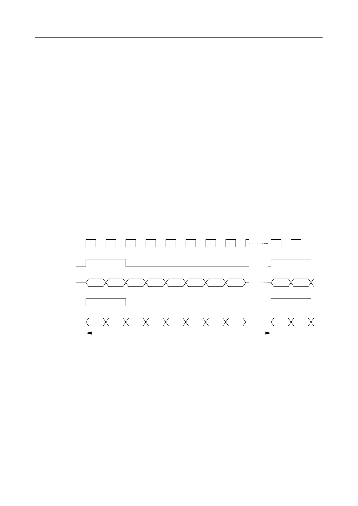
This PCM output signal is output from MSB in synchronization with the rising edge of BCLK or
XSYNC. A pull-up resistor must be connected to this pin, because this output is configuared as
an open drain.
During power down, this output is at high impedance state.
6/25

¡ Semiconductor
MSM7575
PCMRI
Receive PCM data input.
This PCM input signal is shifted on the falling edge of BCLK and input from MSB.
BCLK
Shift clock input for the PCM data (PCMSO, PCMRI).
The frequency is set in the range of 64 kHz to 2048 kHz.
XSYNC
8 kHz synchronous signal input for Transmit PCM data.
This signal should be synchronized with BCLK. XSYNC is used for indicating MSB of the
transmit serial PCM.
Be sure to input the XSYNC signal because it is also used as the input of the timing circuit and
the clock source of the tone generator.
RSYNC
8 kHz synchronous signal input for Receive PCM data.
This signal should be synchronized with BCLK signal. RSYNC is used for indicating the MSB
of the receive serial PCM.
BCLK
XSYNC
PCMSO
RSYNC
PCMRI
MSB LSB
MSB LSB
8kHz
(125ms)
Figure 3 PCM Interface Basic Timing Diagram
7/25

¡ Semiconductor
MSM7575
VOXO
Transmit VOX function signal output.
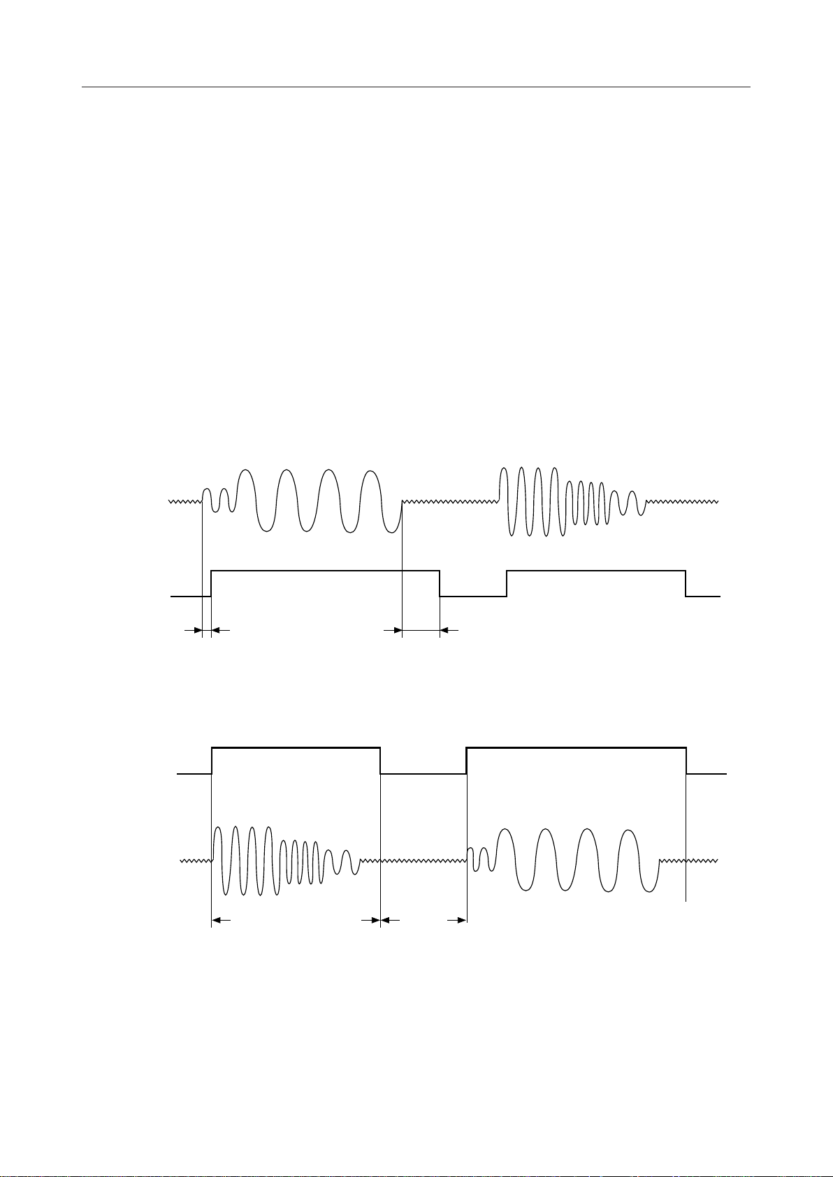
VOX function is to recognize the presence or absence of the transmit voice signal by detecting the
signal energy. “H” and “L” levels set to this pin correspond to the presence and the absence,
respectively. This result appears also at the register data CR7-B7. The signal energy detect
threshold is set by the control register data CR6-B6, B5.
VOXI
Signal input for receive VOX function.
The “H” level at VOXI indicates the presence of voice signal, the decoder block processes normal
receive signal, and the voice signal appears at analog output pins . The “L” level indicates the
absence of voice signal, the background noise generated in this device is transferred to the analog
output pins. The background noise amplitude is set by the control register CR6. Because this
signal is ORed with the register data CR6-B3, the control register data CR6-B3 should be set to
digital “0”.
Voice Input
GSX2
VOXO
VOXI
Voice Output
VFRO
(Absence)
(Presence)
T
VXON
Presence
Detect
T
VXOFF
Absence
Detect (Hang-over time)
(a) Transmit VOX Function Timing Diagram
(Absence)
(Presence)
(Presence)
(Presence)
Normal Voice Signal
Decoded Time period
Background
Noise
(b) Receive VOX Function (CR6-B3: digital "0") Timing Diagram
Note: VOXO, VOXI function become valid when setting CR6-B7 to digital “1”.
Figure 4 VOX Function
8/25
 Loading...