OKI MSM7540GS-K, MSM7560GS-K Datasheet

FEDL7540-03
FEDL7540-03
¡ Semiconductor
¡ Semiconductor
This version: Nov. 1999
Previous version: Aug. 1998
MSM7540/7560
MSM7540/7560
Single Rail ADPCM CODEC
GENERAL DESCRIPTION
The MSM7540/7560 are single channel ADPCM CODEC ICs which perform mutual transcoding
between an analog voice band signal 300 to 3400 Hz and 32 kbps ADPCM serial data.
Using advanced circuit technology, these devices operate using a single 5 V power supply and
have low power consumption.
The MSM7540/7560 are optimized for advanced digital cordless telephone system applications.
FEATURES
••
• Single 5 V Power Supply Operation
••
••
• ADPCM Algorithm : Complies completely with 1988's version ITU-T
••
G.721 (32 kbps)
••
• Transmit/Receive Full-Duplex Operation
••
••
• Transmit/Receive Synchronous Mode Only
••
••
• Serial ADPCM Transmission Data Rate : 32 kbps to 2048 kbps
••
••
• Serial PCM Transmission Data Rate : 64 kbps to 2048 kbps
••
••
• PCM Interface Coding Format
••
MSM7540 : A-law or Linear (14-bit, 2's compliment) Selectable
MSM7560 : m-law or Linear (14-bit, 2's compliment) Selectable
••
• Low Power Consumption
••
Operating Mode : 60 mW Typ.
Power-Down Mode : 1.0 mW Typ.
••
• Two Analog Input Amplifier Stages : Externally Adjustable Gain
••
••
• Analog Output Stage : Push-pull Drive (direct drive of 350 W␣ + 120 nF)
••
••
• Built-in Crystal Oscillator (10.368 MHz)
••
••
• Built-in Reference Voltage Supply
••
••
• Option Reset Specified by ITU-T G. 721/ADPCM
••
••
• Package:
••
28-pin plastic SOP (SOP28-P-430-1.27-K) (Product name: MSM7540GS-K)
(Product name: MSM7560GS-K)
1/16

2/16
MSM7540/7560
¡ Semiconductor
FEDL7540-03
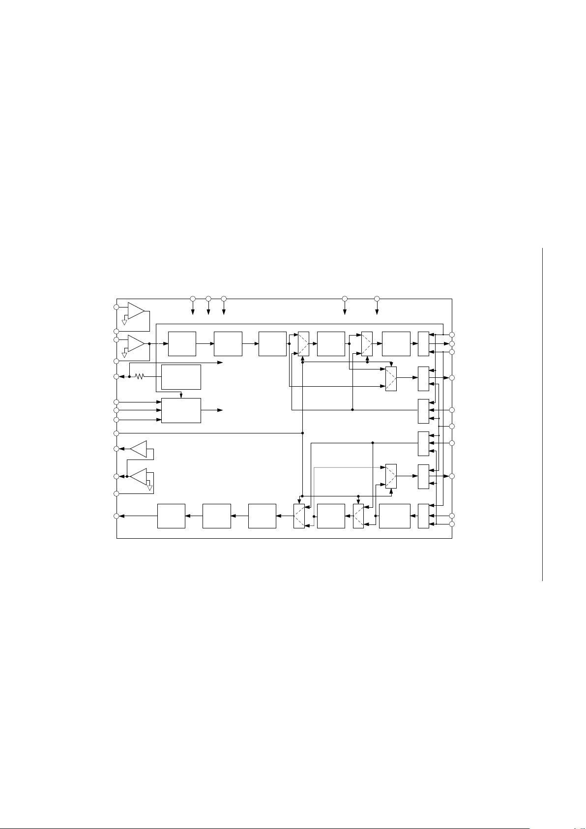
BLOCK DIAGRAM
AIN2
GSX2
XSYNC
IS
AIN1
GSX1
AOUT–
ADPCM
CODER
1
0
V
DD
BCLKA
0
1
PCMSO
PCMSI
PCMRI
PCMRO
IR
RSYNC
0
1
ADPCM
DECODER
1
0
BCLKB
AG DG X1 X2
PWI
V
REF
SG
CLOCK/
TIMING
MCK
LPS
RES
PDN
AOUT+
–
+
–1
VFRO
–
+
–
+
P
/
S
P
/
S
S
/
P
S
/
P
P
/
S
S
/
P
0
1
RCLPF
A/D
Conv.
BPF
EXPANDER
1
0
RCLPF
D/A
Conv.
LPF
COMPANDER

FEDL7540-03
¡ Semiconductor
PIN CONFIGURATION (TOP VIEW)
1
RES
IR
IS
LPS
DG
AG
SG
2
3
4
5
6
7
8
9
10
11
PCMRI
PCMRO
PCMSI
PCMSO
28
27
26
25
24
23
22
21
20
19
18
BCLKB
BCLKA
XSYNC
RSYNC
MCK
X2
X1
PDN
V
DD
AOUT+
AOUT–
MSM7540/7560
12
AIN1
13
GSX1
14 15
AIN2 GSX2
17
16
PWI
VFRO
28-Pin Plastic SOP
3/16

FEDL7540-03
(
)
¡ Semiconductor
MSM7540/7560
PIN AND FUNCTIONAL DESCRIPTIONS
AIN1, AIN2, GSX1, GSX2
Transmit analog inputs and the output for transmit gain adjustment.
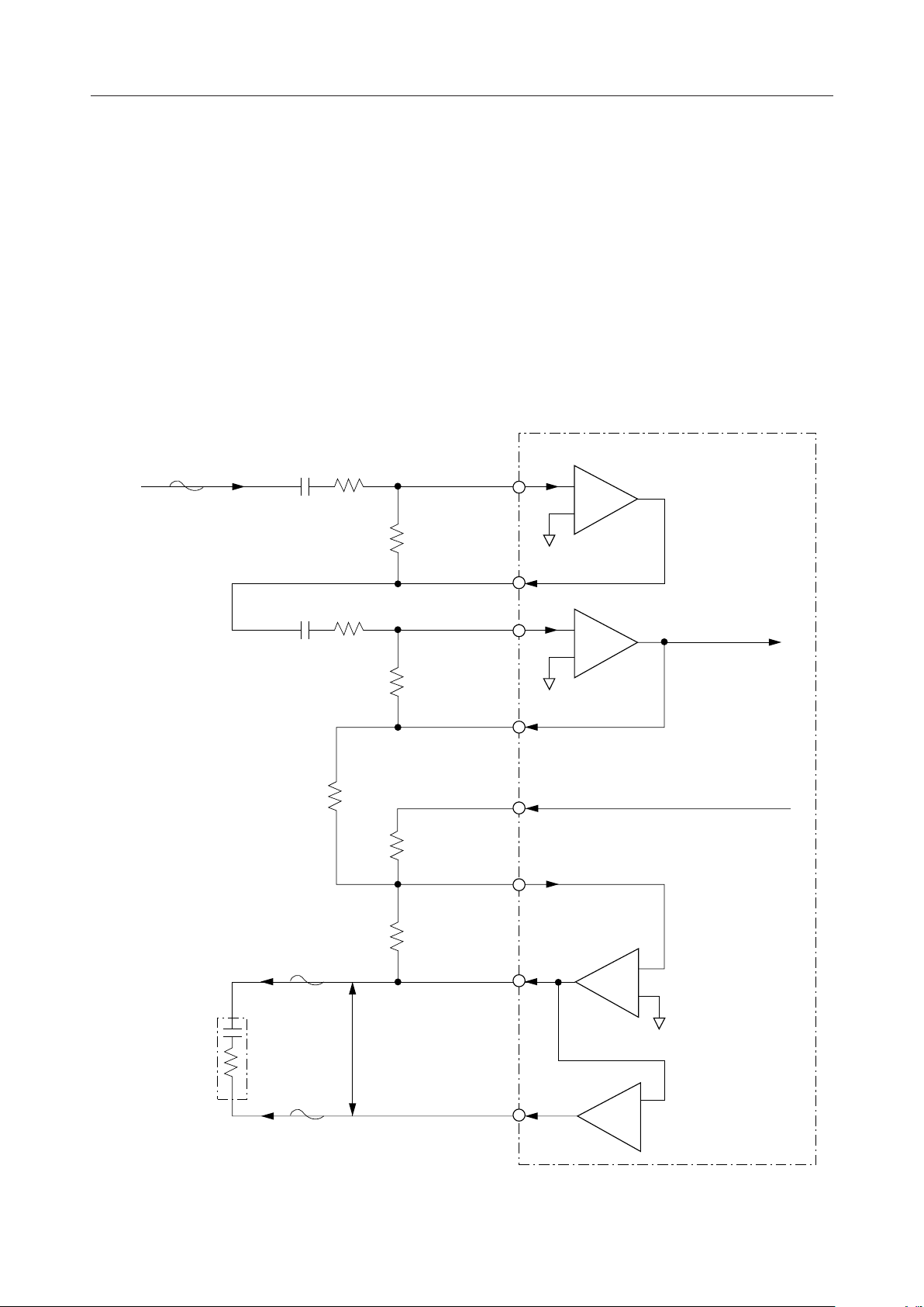
AIN1 (AIN2) connects to the inverting input of the internal transmit amplifier. GSX1 (GSX2)
connects to the internal transmit amplifier output. Refer to Fig. 1 for gain adjustment.
VFRO, AOUT+, AOUT–, PWI
Receive analog output and the output for receive gain adjustment.
VFRO is the receive filter output. AOUT+ and AOUT– are differential analog signal outputs
which can directly drive ZL = 350 W + 120 nF. Refer to Fig. 1 for gain adjustment.
Analog Input
C1
R1
AIN1
–
+
R2
Transmit Gain:
= (R2/R1) ¥ (R4/R3)
Receive Gain:
= (R6/R5)
C2
R3
RS*
R4
R5
R6
GSX1
AIN2
GSX2
VFRO
PWI
AOUT–
–
+
to ENCODER
from DECODER
–
+
V
+ 350 W
Analog OutputZL=120 nF
0
* : Side Tone Pass
Figure 1 Analog Input/Output Interface
–1
AOUT+
Gain = R6/RS
4/16

FEDL7540-03
¡ Semiconductor
MSM7540/7560
SG
Analog signal ground voltage output.
The output voltage of this pin is approximately 2.4 V. Put bypass capacitors between this pin
and the AG pin. During power-down this output voltage is 0 V. The external SG voltage, if
necessary, should be used via a buffer.
AG
Analog ground.
DG
Digital ground.
This ground is separated internally from the analog signal ground pin (AG). The DG pin must
be kept as close as possible to AG on the PCB.
V
DD
+5 V power supply.
LPS
PCM coding law selection.
MSM7540 only ; if this pin goes to a "0" level, PCMSO, PCMSI, PCMRO, and PCMRI become the
A-law character signal, and if these pins goes to a "1" level, the signal becomes a linear value
character signal (2's complement).
MSM7560 only ; if this pin goes to a "0" level, PCMSO, PCMSI, PCMRO, and PCMRI become the
m-law character signal, and if these pins goes to a "1" level, the signal becomes a linear value
character signal (2's complement).
PDN
Power down control input.
If this pin is "0", this device is in the power-down state.
Normally, this pin is set to "1".
RES
Optional reset input specified by ITU-T Recommendation G. 721.
If this pin is "0", the device is in the reset state. The reset width (during "L") should be 125ms or
more.
MCK
Master clock input.
The frequency must be 10.368 MHz. The master clock signal may be asynchronous to BCLKA,
BCLKB, XSYNC, and RSYNC.
PCMSO
Transmit PCM data output.
PCM is output from MSB in synchronization with the rising edge of BCLKB and XSYNC.
5/16
 Loading...